US7830698B2 - Multilevel nonvolatile memory device containing a carbon storage material and methods of making and using same - Google Patents
Multilevel nonvolatile memory device containing a carbon storage material and methods of making and using same Download PDFInfo
- Publication number
- US7830698B2 US7830698B2 US12/153,872 US15387208A US7830698B2 US 7830698 B2 US7830698 B2 US 7830698B2 US 15387208 A US15387208 A US 15387208A US 7830698 B2 US7830698 B2 US 7830698B2
- Authority
- US
- United States
- Prior art keywords
- state
- resistivity
- carbon material
- carbon
- applying
- Prior art date
- Legal status (The legal status is an assumption and is not a legal conclusion. Google has not performed a legal analysis and makes no representation as to the accuracy of the status listed.)
- Active, expires
Links
Images


Classifications
-
- G—PHYSICS
- G11—INFORMATION STORAGE
- G11C—STATIC STORES
- G11C11/00—Digital stores characterised by the use of particular electric or magnetic storage elements; Storage elements therefor
- G11C11/56—Digital stores characterised by the use of particular electric or magnetic storage elements; Storage elements therefor using storage elements with more than two stable states represented by steps, e.g. of voltage, current, phase, frequency
-
- B—PERFORMING OPERATIONS; TRANSPORTING
- B82—NANOTECHNOLOGY
- B82Y—SPECIFIC USES OR APPLICATIONS OF NANOSTRUCTURES; MEASUREMENT OR ANALYSIS OF NANOSTRUCTURES; MANUFACTURE OR TREATMENT OF NANOSTRUCTURES
- B82Y10/00—Nanotechnology for information processing, storage or transmission, e.g. quantum computing or single electron logic
-
- G—PHYSICS
- G11—INFORMATION STORAGE
- G11C—STATIC STORES
- G11C13/00—Digital stores characterised by the use of storage elements not covered by groups G11C11/00, G11C23/00, or G11C25/00
-
- G—PHYSICS
- G11—INFORMATION STORAGE
- G11C—STATIC STORES
- G11C13/00—Digital stores characterised by the use of storage elements not covered by groups G11C11/00, G11C23/00, or G11C25/00
- G11C13/0002—Digital stores characterised by the use of storage elements not covered by groups G11C11/00, G11C23/00, or G11C25/00 using resistive RAM [RRAM] elements
- G11C13/0021—Auxiliary circuits
- G11C13/0069—Writing or programming circuits or methods
-
- G—PHYSICS
- G11—INFORMATION STORAGE
- G11C—STATIC STORES
- G11C13/00—Digital stores characterised by the use of storage elements not covered by groups G11C11/00, G11C23/00, or G11C25/00
- G11C13/02—Digital stores characterised by the use of storage elements not covered by groups G11C11/00, G11C23/00, or G11C25/00 using elements whose operation depends upon chemical change
- G11C13/025—Digital stores characterised by the use of storage elements not covered by groups G11C11/00, G11C23/00, or G11C25/00 using elements whose operation depends upon chemical change using fullerenes, e.g. C60, or nanotubes, e.g. carbon or silicon nanotubes
-
- H—ELECTRICITY
- H10—SEMICONDUCTOR DEVICES; ELECTRIC SOLID-STATE DEVICES NOT OTHERWISE PROVIDED FOR
- H10B—ELECTRONIC MEMORY DEVICES
- H10B63/00—Resistance change memory devices, e.g. resistive RAM [ReRAM] devices
- H10B63/20—Resistance change memory devices, e.g. resistive RAM [ReRAM] devices comprising selection components having two electrodes, e.g. diodes
-
- H—ELECTRICITY
- H10—SEMICONDUCTOR DEVICES; ELECTRIC SOLID-STATE DEVICES NOT OTHERWISE PROVIDED FOR
- H10B—ELECTRONIC MEMORY DEVICES
- H10B63/00—Resistance change memory devices, e.g. resistive RAM [ReRAM] devices
- H10B63/80—Arrangements comprising multiple bistable or multi-stable switching components of the same type on a plane parallel to the substrate, e.g. cross-point arrays
-
- H—ELECTRICITY
- H10—SEMICONDUCTOR DEVICES; ELECTRIC SOLID-STATE DEVICES NOT OTHERWISE PROVIDED FOR
- H10N—ELECTRIC SOLID-STATE DEVICES NOT OTHERWISE PROVIDED FOR
- H10N70/00—Solid-state devices having no potential barriers, and specially adapted for rectifying, amplifying, oscillating or switching
- H10N70/011—Manufacture or treatment of multistable switching devices
- H10N70/021—Formation of switching materials, e.g. deposition of layers
- H10N70/023—Formation of switching materials, e.g. deposition of layers by chemical vapor deposition, e.g. MOCVD, ALD
-
- H—ELECTRICITY
- H10—SEMICONDUCTOR DEVICES; ELECTRIC SOLID-STATE DEVICES NOT OTHERWISE PROVIDED FOR
- H10N—ELECTRIC SOLID-STATE DEVICES NOT OTHERWISE PROVIDED FOR
- H10N70/00—Solid-state devices having no potential barriers, and specially adapted for rectifying, amplifying, oscillating or switching
- H10N70/011—Manufacture or treatment of multistable switching devices
- H10N70/061—Shaping switching materials
- H10N70/063—Shaping switching materials by etching of pre-deposited switching material layers, e.g. lithography
-
- H—ELECTRICITY
- H10—SEMICONDUCTOR DEVICES; ELECTRIC SOLID-STATE DEVICES NOT OTHERWISE PROVIDED FOR
- H10N—ELECTRIC SOLID-STATE DEVICES NOT OTHERWISE PROVIDED FOR
- H10N70/00—Solid-state devices having no potential barriers, and specially adapted for rectifying, amplifying, oscillating or switching
- H10N70/20—Multistable switching devices, e.g. memristors
-
- H—ELECTRICITY
- H10—SEMICONDUCTOR DEVICES; ELECTRIC SOLID-STATE DEVICES NOT OTHERWISE PROVIDED FOR
- H10N—ELECTRIC SOLID-STATE DEVICES NOT OTHERWISE PROVIDED FOR
- H10N70/00—Solid-state devices having no potential barriers, and specially adapted for rectifying, amplifying, oscillating or switching
- H10N70/801—Constructional details of multistable switching devices
- H10N70/821—Device geometry
- H10N70/826—Device geometry adapted for essentially vertical current flow, e.g. sandwich or pillar type devices
- H10N70/8265—Device geometry adapted for essentially vertical current flow, e.g. sandwich or pillar type devices on sidewalls of dielectric structures, e.g. mesa-shaped or cup-shaped devices
-
- H—ELECTRICITY
- H10—SEMICONDUCTOR DEVICES; ELECTRIC SOLID-STATE DEVICES NOT OTHERWISE PROVIDED FOR
- H10N—ELECTRIC SOLID-STATE DEVICES NOT OTHERWISE PROVIDED FOR
- H10N70/00—Solid-state devices having no potential barriers, and specially adapted for rectifying, amplifying, oscillating or switching
- H10N70/801—Constructional details of multistable switching devices
- H10N70/881—Switching materials
- H10N70/884—Switching materials based on at least one element of group IIIA, IVA or VA, e.g. elemental or compound semiconductors
- H10N70/8845—Carbon or carbides
-
- G—PHYSICS
- G11—INFORMATION STORAGE
- G11C—STATIC STORES
- G11C13/00—Digital stores characterised by the use of storage elements not covered by groups G11C11/00, G11C23/00, or G11C25/00
- G11C13/0002—Digital stores characterised by the use of storage elements not covered by groups G11C11/00, G11C23/00, or G11C25/00 using resistive RAM [RRAM] elements
- G11C13/0021—Auxiliary circuits
- G11C13/0069—Writing or programming circuits or methods
- G11C2013/009—Write using potential difference applied between cell electrodes
-
- G—PHYSICS
- G11—INFORMATION STORAGE
- G11C—STATIC STORES
- G11C2213/00—Indexing scheme relating to G11C13/00 for features not covered by this group
- G11C2213/30—Resistive cell, memory material aspects
- G11C2213/35—Material including carbon, e.g. graphite, grapheme
-
- G—PHYSICS
- G11—INFORMATION STORAGE
- G11C—STATIC STORES
- G11C2213/00—Indexing scheme relating to G11C13/00 for features not covered by this group
- G11C2213/70—Resistive array aspects
- G11C2213/72—Array wherein the access device being a diode
-
- G—PHYSICS
- G11—INFORMATION STORAGE
- G11C—STATIC STORES
- G11C2213/00—Indexing scheme relating to G11C13/00 for features not covered by this group
- G11C2213/70—Resistive array aspects
- G11C2213/79—Array wherein the access device being a transistor
Definitions
- the invention relates to a nonvolatile memory array.
- Nonvolatile memory arrays maintain their data even when power to the device is turned off.
- each memory cell is formed in an initial unprogrammed state, and can be converted to a programmed state. This change is permanent, and such cells are not erasable. In other types of memories, the memory cells are erasable, and can be rewritten many times.
- Cells may also vary in the number of data states each cell can achieve.
- a data state may be stored by altering some characteristic of the cell which can be detected, such as current flowing through the cell under a given applied voltage or the threshold voltage of a transistor within the cell.
- a data state is a distinct value of the cell, such as a data ‘0’ or a data ‘1’.
- Floating gate and SONOS memory cells operate by storing charge, where the presence, absence or amount of stored charge changes a transistor threshold voltage. These memory cells are three-terminal devices that are relatively difficult to fabricate and operate at the very small dimensions required for competitiveness in modern integrated circuits.
- nonvolatile memory array having erasable or multi-state memory cells formed using semiconductor materials in structures that are readily scaled to small size and having a capacity of more than 1 bit/cell (i.e., ⁇ 2 bits/cell) is desirable.
- An embodiment of the invention provides nonvolatile memory cell which includes a steering element located in series with a storage element.
- the storage element includes a carbon material and the memory cell includes a rewritable cell having multiple memory levels.
- FIG. 1 is a circuit diagram illustrating the need for electrical isolation between memory cells in a memory array.
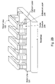
- FIGS. 2A and 2F are perspective views of a memory cell formed according to an embodiment of the present invention.
- FIGS. 2B-2E are perspective views of memory cell arrays formed according to embodiments of the present invention.
- FIGS. 3A-3B are side cross-sectional views illustrating two embodiments of a memory cell.
- FIGS. 4A-4D are schematic side cross-sectional views illustrating alternative diode configurations according to an embodiment of the present invention.
- FIGS. 5A and 5B are circuit diagrams showing reading and programming operations.
- FIGS. 6A and 6B are current-voltage plots
- FIGS. 6C , 6 E, 7 A, 7 B and 7 C are probability plots showing reading of cells
- FIG. 6D is a probability plot of programming voltage of a cell of the embodiments of the invention.
- FIG. 7D is a circuit schematic of a device of an embodiment of the invention.
- FIGS. 7E and 7F are plots of voltage versus time for programming a device of an embodiment of the invention.
- FIGS. 8A to 8K illustrate one exemplary method of making an array of memory cells shown in FIG. 2D .
- FIG. 9 is a Raman spectrum of polycrystalline carbon of an embodiment of the invention.
- trimmable resistors have been used as elements in integrated circuits.
- resistors are used as memory cells in a large cross-point array, when voltage is applied to a selected cell, there will be undesired leakage through half-selected and unselected cells throughout the array. For example, turning to FIG. 1 , suppose a voltage is applied between bitline B and wordline A to set, reset, or sense selected cell S. Current is intended to flow through selected cell S. Some leakage current, however, may flow on alternate paths, for example between bitline B and wordline A through unselected cells U 1 , U 2 , and U 3 . Many such alternate paths may exist.
- Leakage current can be greatly reduced by forming each memory cell with a steering element, such as a transistor or a diode.
- a diode has a non-linear I-V characteristic, allowing very little current flow below a turn-on voltage, and substantially higher current flow above the turn-on voltage.
- a diode also acts as one-way valves passing current more easily in one direction than the other.
- transition from a higher- to a lower-resistivity state will be called a set transition, affected by a set current, a set or programming voltage, or a set or programming pulse; while the reverse transition, from a lower- to a higher-resistivity state, will be called a reset transition, affected by a reset current, a reset voltage, or a reset pulse which places the diode in an unprogrammed state.
- the memory cell includes a steering element, such as a transistor or a diode, and a storage element, such as a carbon resistivity switching material.
- the steering element comprises a diode and the carbon resistivity switching material comprises polycrystalline carbon, amorphous carbon, graphene or carbon nanotubes (single walled, multi-walled or a mixture of single and multi-walled nanotubes).
- the diode comprises a cylindrical semiconductor diode which is located in series with a cylindrical carbon resistivity switching material layer, film or region. The diode and the resistivity switching material are disposed between two electrodes, as illustrated in FIG. 2A .
- the diode and resistivity switching material may have a shape other than cylindrical, if desired.
- a memory cell comprising a diode and a resistivity switching material
- U.S. patent application Ser. No. 11/125,939 filed on May 9, 2005 which corresponds to US Published Application No. 2006/0250836 to Herner et al.
- U.S. patent application Ser. No. 11/395,995 filed on Mar. 31, 2006 which corresponds to US Patent Published Application No. 2006/0250837 to Herner et al., each of which is hereby incorporated by reference.
- FIG. 2A illustrates the perspective view of a memory cell formed according to a preferred embodiment of the present invention.
- a bottom conductor 101 is formed of a conductive material, for example tungsten, and extends in a first direction. Barrier and adhesion layers, such as TiN layers, may be included in bottom conductor 101 .
- the semiconductor diode 110 has a bottom heavily doped n-type region 112 ; an intrinsic region 114 , which is not intentionally doped; and a top heavily doped p-type region 116 , though the orientation of this diode may be reversed, as shown in FIGS. 4 a to 4 d .
- Such a diode regardless of its orientation, will be referred to as a p-i-n diode or simply diode.
- the storage element such as the carbon resistivity switching material 118 is disposed above or below the diode.
- material 118 may be disposed on the p-type region 116 or below the n-region 112 of the diode 110 , as shown for example in FIGS. 3A and 3B .
- An optional intermediate conductive layer, such as a TiN layer, may be disposed between the diode 110 and the material 118 .
- Top conductor 100 may be formed in the same manner and of the same materials as bottom conductor 101 , and extends in a second direction different from the first direction.
- the semiconductor diode 110 is vertically disposed between bottom conductor 101 and top conductor 100 (i.e., electrodes 101 and 100 ).
- the diode can comprise any single crystal, polycrystalline, or amorphous semiconductor material, such as silicon, germanium, or silicon-germanium alloys.
- the memory cell shown in FIG. 2A comprises a vertical two terminal cell containing the two-terminal based diode steering element.
- a three-terminal cell containing a transistor steering element may also be used.
- the conductive path between the electrodes can be either a vertical one, a side-wall vertical one, a combination of vertical and lateral one, or a combination of vertical and lateral one with an adhesion layer, as will be described in more detail below.
- the diode 110 comprises three different regions 112 , 114 , 116 .
- a region of semiconductor material which is not intentionally doped is described as an intrinsic region 114 as shown in FIG. 2A and FIGS. 3A-B .
- an intrinsic region may in fact include a low concentration of p-type or n-type dopants. Dopants may diffuse into the intrinsic region from the adjacent n or p-doped regions ( 112 and 116 , respectively in FIG. 3A and 3B ) or may be present in the deposition chamber during deposition due to contamination from an earlier deposition.
- deposited intrinsic semiconductor material may include defects which cause it to behave as if slightly n-doped.
- intrinsic semiconductor to describe silicon, germanium, a silicon-germanium alloy, or some other semiconductor material is not meant to imply that this region contains no dopants whatsoever, nor that such a region is perfectly electrically neutral.
- the diode need not be limited to a p-i-n design as described; rather, a diode can comprise a combination of the different regions, each with different concentrations of dopants, as illustrated in FIGS. 4A-4D .
- FIGS. 4A-4D Various additional cell structures and methods of making the memory cell will be described in more detail below.
- amorphous or microcrystalline silicon When amorphous or microcrystalline silicon is crystallized in contact with one of these silicides, the crystal lattice of the silicide provides a template to the silicon during crystallization.
- the resulting polysilicon will be highly ordered, and relatively low in defects.
- This high-quality polysilicon when doped with a conductivity-enhancing dopant, is relatively highly conductive as formed.
- Such a diode preferably acts as a steering element of the memory cell because the diode does not change resistivity when certain voltage pulses are applied which are sufficient to switch the resistivity state of the carbon material.
- amorphous or microcrystalline silicon material when crystallized not in contact with a silicide with which it has a good lattice match, for example when silicon is crystallized in contact only with materials such as silicon dioxide and titanium nitride, with which it has a significant lattice mismatch, the resulting polysilicon will have many more defects, and doped polysilicon crystallized this way will be much less conductive as formed.
- Such diode can switch resistivity state when bias is applied.
- the diode can also serve as a resistivity switching element and as the steering element of the memory cell.
- FIGS. 2B to 2E illustrate various embodiments of an array of memory cells.
- the diode steering element 110 is omitted from these figures for clarity. However, it should be understood that the diode steering element is located either above or below the storage element, such as the carbon resistivity switching material 118 , as shown in FIG. 2A .
- a feature 204 such as an insulating material feature is formed above or below the diode.
- the feature may comprise any suitable pillar, post or rail or even a sidewall of a via or trench made of any suitable insulating material, such as silicon oxide, silicon nitride, organic insulating material, etc.
- the feature may have any suitable height, such as greater than 40 nm, such as 50-500 nm, for example 200-300 nm.
- the carbon resistivity switching material 118 is disposed on the sidewall(s) and over the top of this feature as a thin film or layer.
- This film or layer may have any suitable thickness, such as 2-10 nm, and a height which corresponds to the height of the feature 204 (i.e., preferably over 40 nm).
- the material 118 generally has a sidewall spacer shape on the sidewall of the feature.
- An optional adhesion layer 206 such as a silicon oxynitride or titanium nitride material is disposed on top and/or on the sides of the feature to promote adhesion between the feature and the carbon material. As shown in FIG. 2C , the adhesion layer may be omitted.
- the carbon resistivity switching material 118 in FIGS. 2B and 2C provides both a vertical conductive path (via the sidewall component) and a lateral (horizontal) conductive path between the upper and lower electrodes. As shown in FIG. 2D , the carbon resistivity switching material 118 is located only on the sidewall of the feature and thus provides only a vertical sidewall conductive path. A method of making this structure will be described in more detail below with respect to FIGS. 8A-8K .
- FIG. 2E shows an alternative structure, where the carbon resistivity switching material 118 is deposited into an opening, such as a trench or via in an insulating layer (not shown for clarity).
- the material 118 may be deposited by spray coating or spin coating a slurry or colloid containing the carbon material.
- the carbon resistivity switching material 118 comprises a block or rail of material which provides a bulk vertical conductive path.
- a height of the resistivity switching material 118 in a first direction from the first conductive electrode 101 to the second conductive electrode 100 may be greater than a thickness of the resistivity switching material in second direction perpendicular to the first direction.
- the material 118 comprises a thin film or layer, then the thickness of at least a portion of the film or layer is oriented in a perpendicular direction to the current flow direction between the electrodes 100 and 101 .
- FIG. 2F shows a schematic of the memory cell test structure which corresponds to the layout of FIG. 2B , in which the p+ region 116 of the diode 110 is located below the feature 204 and the adhesion layer 206 .
- the carbon resistivity switching material 118 is located on the sidewalls of the feature and over the adhesion layer and electrically contacts the upper p+ region of the diode 110 .
- a diode formed of polycrystalline silicon and a polycrystalline carbon storage material i.e., the resistivity switching material
- the memory cell may be a one time programmable (OTP) cell.
- OTP one time programmable
- one-time programmable means that cell can be non-reversibly programmed into up to four different states.
- the cell is preferably a multi level cell (MLC) rewritable memory cell which has two or more distinct memory levels or states, such as two to four levels, which can be reversibly programmed.
- MLC multi level cell
- the cell is rewritable cell having multiple memory levels and during programming, the cell is placed into at least two different memory levels for at least two programming cycles.
- the MLC writable memory cell provides a high density and a simplified architecture and process.
- the device in preferred embodiments, has four distinct data states (i.e., memory levels).
- the difference between the read currents of the unprogrammed and various programmed states constitutes the “window” for the memory cell. It is desirable for this window to be as large as possible for manufacturing robustness.
- the present inventors realized that the read current window of the programmed cell and the number of bits per cell can be increased by the following programming method.
- Distinct data states of the memory cell of the embodiments of the present invention correspond to resistivity states of the carbon based storage material in series with the diode.
- the memory cell can be put into distinct data states by a series of distinct forward biases, preferably ranging from 2 to 20 V, more preferably from 6 to 18 V.
- the current flowing through the cell between any one distinct data state and any different distinct data state is different by at least a factor of two, to allow the difference between the states to be readily detectable.
- FIG. 5A shows biasing the array of memory cells in a read mode.
- Vrd(Vux) applied to selected bit line and unselected word lines is about 0.8 to about 2.3V (selectable by option-bits) while Vub applied to unselected bit lines and to the selected word line is zero volts.
- Vrd(Vux) applied to selected bit line and unselected word lines is about 0.8 to about 2.3V (selectable by option-bits) while Vub applied to unselected bit lines and to the selected word line is zero volts.
- a forward bias is applied to the cell having a magnitude greater than a minimum voltage required for programming the cell.
- FIG. 5B shows biasing the array in a write-mode, as will be described in more detail below.
- the minimum voltage required to program the cell is 16 V
- a programming forward bias of 16 or more volts, such as about 18 V to about 20 V is applied to the selected cells.
- the maximum voltage which can be applied without damaging the diode may be used as the programming voltage.
- FIGS. 6A and 6B are current-voltage (IV) plots and FIG. 6C is a probability plot showing read current of a test structure memory cell shown in FIG. 2F containing a p++ single crystal silicon layer and a polycrystalline carbon storage element at 1V read voltage (at 200° C. with flowing nitrogen) in various states.
- the polycrystalline carbon is deposited at 700° C. over the 200 nm silicon oxide feature topped with a 100 nm thick metal (chromium) adhesion layer for one minute using thermal CVD with H 2 and C 2 H 2 source gases in a 3:1 ratio. It should be noted that this device was constructed for test purposes and that a diode may be included instead of the p++ region in a memory cell.
- FIG. 6A shows the IV curve from the first device site and FIG. 6B shows the device curve from the second device site.
- the plot in FIG. 6C provides the results from both sites with two cycles for each site.
- the IV curves in FIGS. 6A and 6B indicate read current levels after each programming pulse operation.
- the read current has been swept from 0 ⁇ 1.5V.
- the device was exposed to two programming cycles performed as follows. There is no state being changed to be observed for the read voltage less than 1.5V.
- the initial read current is about 200 ⁇ A at 1V (such as between 219 and 285 ⁇ A).
- An initial high voltage reset pulse such as an 18V pulse with a 100 ⁇ S pulse width or duration is used to reset the device to the first memory level or state.
- the read current at 1V is less that 5 ⁇ A (such as about 0.5 to about 2.4 ⁇ A).
- a first set pulse such as a 6V set pulse with about 1 to 10 ⁇ S pulse width is used to set the device to the second memory level.
- the read current at 1V is less than 50 ⁇ A (such as about 9 to 24 ⁇ A).
- a second set pulse such as a 8V pulse with about 10 to 200 ⁇ S pulse width is used to set the device to the third level.
- the read current at 1V is less than 150 ⁇ A (such as about 60 to 118 ⁇ A).
- a third set pulse such as a 10V pulse with an about 100 mS pulse width is used to set the device to the fourth (or initial) memory level.
- the read current at 1V is above 150 ⁇ A (such as about 170 to 272 ⁇ A).
- the read current measured from the first and the second sites on the device after each programming pulse is shown in Tables I and II, respectively.
- FIGS. 6A-6C and in Tables I and II the read current at both sites in the device is similar after the first and the second programming cycles. Also, both sites have the consistent behavior to indicate this memory cell is a MLC writable memory cell.
- FIG. 6D shows the probability plot of the set and reset pulse voltages for 2000 programming cycles.
- FIG. 6E shows the probability plot of the read current at 0.5V.
- the set pulses had a 100 millisecond pulse duration and the reset pulses had a 100 nanosecond pulse duration.
- the device tested contained a 40 nm thick polycrystalline carbon film with a 100 ohm resistance in series. This shows that the test device can be cycled for at least 2000 cycles without failure. Other voltages and pulse durations may be used, depending on the materials used and device design.
- the following non-limiting values of the applied voltage may be applied to the bit lines and word lines, where Vwr is applied to the selected bit line, Vux is applied to unselected word lines and Vub is applied to the unselected bit lines (and zero volts applied to the selected word line).
- a lower voltage may also be used, such as in the final set programming step.
- the reset pulse may have a higher voltage than some or all of the set pulses.
- Each set pulse may optionally but not necessarily have a higher voltage and a longer pulse width than a preceding set pulse.
- the set and reset pulses are forward bias pulses with respect to the diode 110 .
- One advantage of the above described memory cell is that its read current levels can be well defined with pulse width and pulse amplitude.
- one or more initialization pulses are used to in the method of programming the device. Due to the complexity of the carbon resistivity switching material, such as nanotubes, amorphous carbon, polycrystalline carbon or graphene, the time needed to program and erase CNT or carbon film is in the order of milliseconds (msec) using a conventional operation algorithm.
- a stepped voltage amplitude and/or a stepped pulse width can be used during programming. However, these steps enlarge the distribution of operation condition. As resistivities of the rewritable elements are dependent on the electrical signals, it also introduces a wide distribution of on/off current, which makes the on/off windows smaller.
- a relatively high voltage amplitude and relatively long duration initialization pulse is applied first to the carbon resistivity switching material. Thereafter, shorter duration programming pulses are applied to the material to program the memory cell. This allows programming the cell at much higher speeds and hence meet the product bandwidth requirements. Also, the initialization pulse helps to improve the distribution of operation condition, therefore, the distribution of On/Off current.
- the initialization pulse has a pulse width that is 1 millisecond or greater, such as 2-200 ms.
- the initialization pulse voltage amplitude is preferably at least 10V, such as 10 to 14V, for example 10 to 12V (i.e., an initialization set pulse). Other pulse duration and voltages may also be used.
- Plural initialization pulses may also be used, such that an initialization reset pulse having a voltage amplitude of 10 to 20V may follow the set initialization pulse.
- the first reset pulse does not have to be an initialization pulse and may have a pulse width of less than 1 ms.
- the subsequent programming pulses such as reset and/or set pulse preferably have a pulse width of less than 1 ms, such as 100 nm to 500 microseconds, such as 10 to 200 microseconds, for example about 100 microseconds.
- the set pulses preferably have a lower voltage amplitude than the initialization pulse.
- the initialization pulse provides the following effect to the device.
- the current understanding of switching in carbon nanotubes is the mechanical switching through Van der Waals force or electrical switching through quantum wave of overlapping.
- the current understanding of switching in polycrystalline carbon or graphene is related to the change in hybridization of the C—C bonds or the variation in distance between the graphene flakes. It is believed that the relatively wide (i.e., long duration) initialization pulse connects the carbon nanotubes or carbon flakes in the respective carbon material to make the carbon material more uniform (i.e., more compressed or fused together). This improves the electrical connection through each cell between the upper and lower electrodes.
- the initialization improves distribution of set and reset operation range and also that of On and Off read current by reducing the impact from the random distribution of geometries and structures of the carbon films due to their intrinsic material properties.
- the initialization pulse width and pulse amplitude should be in a range to make all the possible conductive paths in the array connected.
- FIG. 7A shows a probability plot for a rewritable nonvolatile memory device described above containing polycrystalline carbon resistivity switching films grown at 700 C for 1 minute. This device was not subject to an initialization pulse.
- the reset pulse width is 200 ms and the reset pulse voltage amplitude is 18V.
- the set pulse width is 100 ms and the set pulse voltage amplitude is 10V.
- FIG. 7B shows a probability plot of a similar device after an initialization pulse has been applied. Specifically, a 10V, 200 ms long initialization pulse followed by an 18V, 200 microsecond reset pulse are provided to the device during the initialization period. Thereafter, 100 microsecond set and reset pulses (having a voltage amplitude of 10V and 18V, respectively) are applied for 10 cycles. As shown in FIG. 7B , the reset and set pulse width can be reduced to less than 1 ms (100 microseconds as shown in this Figure) after the initialization pulse while maintaining a similar read current profile to the device of FIG. 7
- FIG. 7C shows a probability plot of a device that undergone 50 programming cycles (i.e., each memory level was reached 50 times). The initialization pulse is re-applied after every 10 cycles. The device exhibits an acceptable read current distribution. The initialization pulse may be reapplied between every 2 to 50 cycles, such as every 5 to 20 cycles, depending on the device and programming parameters.
- a current limiting device 250 such as a transistor or a resistor is provided between the voltage source 300 and the memory device 110 , 118 .
- the current limiting device decreases or prevents disturbance of the carbon material during the relatively high voltage reset step by limiting the current to the carbon material during the reset step. This allows the improvement from the initialization to be more pronounced in terms of speed performance, On/Off read current distribution, and set/reset operation distribution.
- the set and/or reset pulses may be stepped in regard to voltage amplitude and/or pulse duration.
- FIG. 7E shows a plot of voltage amplitude versus time to illustrate stepped pulse width set and reset pulse trains.
- FIG. 7F shows a plot of voltage amplitude versus time to illustrate stepped voltage amplitude set and reset pulse trains. Both pulse amplitude and width may be stepped at the same time.
- a read step may be performed after each individual pulse to verify the On/Off condition.
- a relatively large and long initialization pulse is used to make all the possible conductive paths connected.
- a current limiting device such as a transistor or any other load to limit the current to a desired range during the reset process, keeps the switching path only at the highest possible conductive path. Therefore, it has the potential to improve the yield, cycling, set/reset operation distribution, on/off read current window, and especially speed performance.
- a device for programming the memory cells is a driver circuit ( 300 in FIG. 7D ) located under, over, or adjacent to the memory cell.
- the circuit can have a monolithic integrated structure, or a plurality of integrated device packaged together or in close proximity or die-bonded together.
- the driver circuit see for example, U.S. patent application Ser. No. 10/185,508 by Cleeves; U.S. patent application Ser. No. 09/560,626 by Knall; and U.S. Pat. No. 6,055,180 to Gudensen et al., each of which is hereby incorporated by reference.
- the memory cell may be fabricated by any suitable methods.
- the methods described U.S. patent application Ser. No. 11/125,939 filed on May 9, 2005 which corresponds to US Published Application No. 2006/0250836 to Herner et al.
- U.S. patent application Ser. No. 11/395,995 filed on Mar. 31, 2006 which corresponds to US Patent Published Application No. 2006/0250837 to Herner et al., which are incorporated by reference in their entirety may be used.
- FIGS. 8A to 8K illustrate one exemplary method of making an array of memory cells shown in FIG. 2D .
- the diode 110 semiconductor layers 112 , 114 , 116 are formed over a lower electrode 101 using any suitable deposition and patterning methods, including in-situ doping during deposition and/or ion implantation into an intrinsic region.
- the diode 110 and lower electrodes 101 are then patterned either sequentially or in the same step, as shown in FIG. 8B .
- the diodes are formed in shape of a cylindrical pillar and the lower electrodes comprise rails (which extend in and out of the page and connect plural diodes).
- a gap fill insulating layer 200 such as silicon oxide, silicon nitride, organic insulating material, etc. is formed between the lower electrodes and the diodes and is then planarized. This step is shown in FIG. 8C .
- the insulating layer may be formed in two separate steps as follows. The lower portion is formed between the electrodes first, followed by planarization step (such as a chemical mechanical polishing (CMP) or etchback step), followed by diode formation, followed by forming the upper portion of the insulating layer between the diodes, and followed by another planarization step.
- planarization step such as a chemical mechanical polishing (CMP) or etchback step
- insulating layer 202 such as silicon oxide, silicon nitride, organic insulating material, etc.
- This insulating layer is then patterned into features 204 having any suitable shape, such as pillars, rails, blocks, etc, as shown in FIG. 8E .
- the upper surface of the diode 110 is partially or fully exposed between the features. For example, each feature may be located in every other space between the diodes (i.e., over each second of the insulating layer 200 located between the diodes 110 ).
- the carbon resistivity switching material 118 film or layer is deposited over the features and on the sidewalls of the features.
- the film 118 may be formed by thermal CVD growth (1-2 minutes at 650 to 800 C using H 2 and C 2 H 2 source gases for polycrystalline carbon) or by spray coating or spin coating a colloid or slurry of nanotubes, graphene or polycrystalline carbon in a solvent.
- the Raman spectrum of the CVD deposited polycrystalline carbon material is shown in FIG. 9 .
- the spectrum has a first Raman peak between 1300 and 1350 cm ⁇ 1 (around 1325 cm ⁇ 1 ) and a second Raman peak between 1600 and 1650 cm ⁇ 1 (around 1625 cm ⁇ 1 ).
- the film or layer 118 may be subjected to a spacer type etch to remove it's portions from the upper surface of regions 200 . This etch makes the film 118 discontinuous, such that the portion of thin film 118 storage element in one cell does not contact a portion of the thin film 118 storage element of an adjacent cell.
- an optional adhesion layer 206 such as silicon oxynitride or another suitable material is deposited over the film 118 , as shown in FIG. 8G .
- the adhesion layer may also be located over each feature, such that it would be located under the carbon film 118 .
- TiN or other materials may also be used instead of SiON for layer 206 .
- gap fill insulating layer 208 (such as silicon oxide, silicon nitride, organic insulating material, etc.) is deposited over the carbon film 118 and the adhesion layer, as shown in FIG. 8H .
- This gap fill insulating layer is then planarized by CMP or etchback with the upper surface of the features 204 to form gap fill insulating regions 210 , as shown in FIG. 8I .
- the carbon film 118 and the adhesion layer are removed from the upper surface of each feature.
- the carbon film 118 remains only on the sidewalls of the features and the upper surface or edges of the carbon film sidewalls 118 A are exposed between the features and the gap fill insulating regions.
- each carbon film sidewall 118 A contacts the upper surface (i.e., the p+ region 116 for example) of the diode 110 .
- the adhesion layer 206 A is located between the carbon sidewalls and the planarized gap fill dielectric regions.
- the upper conductive layer 212 is then deposited over the structure. This conductive layer is then patterned into rail shaped upper electrodes 100 which electrically contact the exposed upper portions of the carbon sidewalls 118 A, as shown in FIG. 8K . As noted above, the film 118 A may be located below the diodes 110 in an alternative configuration. Furthermore, additional layers may be inserted between the above described elements. However, if these intervening layers are conductive, then the above described are still electrically connected to each other.
- the semiconductor material is formed in openings in an insulating layer. This can be performed by either selectively depositing the semiconductor material into openings in the insulating layer or the semiconductor material is non-selectively deposited into openings in the insulating layer and over the upper surface of the insulating layer and then planarized, as described in U.S. application Ser. No. 12/007,780 and U.S. application Ser. No. 12/007,781, both filed on Jan. 15, 2008, which are hereby incorporated by reference in their entirety.
- the carbon film 118 may also be deposited into the openings in the insulating layer, such that the film 118 forms a sidewall spacer on a portion of the sidewall of the opening, followed by the planarization step. In this case, the features may be omitted.
- the upper electrodes 100 may also be formed in the openings by a damascene process.
- FIGS. 2B-2E may be located in a one memory level device. If desired, additional memory levels can be formed above the first memory level to form a monolithic three dimensional memory array. In some embodiments, conductors can be shared between memory levels; i.e. top conductor 100 shown in FIG. 2A would serve as the bottom conductor of the next memory level. In other embodiments, an interlevel dielectric (not shown) is formed above the first memory level, its surface planarized, and construction of a second memory level begins on this planarized interlevel dielectric, with no shared conductors.
- a monolithic three dimensional memory array is one in which multiple memory levels are formed above a single substrate, such as a wafer, with no intervening substrates.
- the layers forming one memory level are deposited or grown directly over the layers of an existing level or levels.
- stacked memories have been constructed by forming memory levels on separate substrates and adhering the memory levels atop each other, as in Leedy, U.S. Pat. No. 5,915,167, “Three dimensional structure memory.”
- the substrates may be thinned or removed from the memory levels before bonding, but as the memory levels are initially formed over separate substrates, such memories are not true monolithic three dimensional memory arrays.
- a monolithic three dimensional memory array formed above a substrate comprises at least a first memory level formed at a first height above the substrate and a second memory level formed at a second height different from the first height. Three, four, eight, or indeed any number of memory levels can be formed above the substrate in such a multilevel array.
- the storage element (such as the resistivity switching material 118 ) has been described as a carbon material above, it may comprise other materials, such as an antifuse dielectric, a fuse, a polysilicon memory effect material, a metal oxide or switchable complex metal oxide material, a phase change material, a conductive bridge element, an electrolyte switching material, or a switchable polymer material.
Landscapes
- Engineering & Computer Science (AREA)
- Chemical & Material Sciences (AREA)
- Nanotechnology (AREA)
- Manufacturing & Machinery (AREA)
- Physics & Mathematics (AREA)
- Mathematical Physics (AREA)
- Theoretical Computer Science (AREA)
- Crystallography & Structural Chemistry (AREA)
- Computer Hardware Design (AREA)
- Semiconductor Memories (AREA)
Abstract
Description
| TABLE I |
| |
| 18 V 100 |
6 |
8 |
10 V 100 mS | ||
| 1st level | 2nd level | 3rd level | 4th level | ||
| 2.19E−04 | ||||
| 1st cycle | 1.54E−06 | 1.65E−05 | 9.00E−05 | 2.25E−04 |
| 2nd cycle | 1.48E−06 | 9.42E−06 | 6.91E−05 | 1.72E−04 |
| TABLE II |
| |
| 18 V 100 |
6 |
8 |
10 V 100 mS | ||
| 1st level | 2nd level | 3rd level | 4th level | ||
| 2.85E−04 | ||||
| 1st cycle | 4.52E−07 | 2.34E−05 | 1.03E−04 | 2.44E−04 |
| 2nd cycle | 2.38E−06 | 2.17E−05 | 1.18E−04 | 2.72E−04 |
Claims (25)
Priority Applications (3)
| Application Number | Priority Date | Filing Date | Title |
|---|---|---|---|
| US12/153,872 US7830698B2 (en) | 2008-04-11 | 2008-05-27 | Multilevel nonvolatile memory device containing a carbon storage material and methods of making and using same |
| PCT/US2009/039120 WO2009126489A1 (en) | 2008-04-11 | 2009-04-01 | Multilevel nonvolatile memory device containing a carbon storage material and methods of making and using same |
| TW98112109A TW200952159A (en) | 2008-04-11 | 2009-04-10 | Multilevel nonvolatile memory device containing a carbon storage material and methods of making and using same |
Applications Claiming Priority (2)
| Application Number | Priority Date | Filing Date | Title |
|---|---|---|---|
| US7109208P | 2008-04-11 | 2008-04-11 | |
| US12/153,872 US7830698B2 (en) | 2008-04-11 | 2008-05-27 | Multilevel nonvolatile memory device containing a carbon storage material and methods of making and using same |
Publications (2)
| Publication Number | Publication Date |
|---|---|
| US20090257265A1 US20090257265A1 (en) | 2009-10-15 |
| US7830698B2 true US7830698B2 (en) | 2010-11-09 |
Family
ID=41163851
Family Applications (1)
| Application Number | Title | Priority Date | Filing Date |
|---|---|---|---|
| US12/153,872 Active 2028-09-17 US7830698B2 (en) | 2008-04-11 | 2008-05-27 | Multilevel nonvolatile memory device containing a carbon storage material and methods of making and using same |
Country Status (1)
| Country | Link |
|---|---|
| US (1) | US7830698B2 (en) |
Cited By (47)
| Publication number | Priority date | Publication date | Assignee | Title |
|---|---|---|---|---|
| US20100157651A1 (en) * | 2008-12-18 | 2010-06-24 | Sandisk 3D Llc | Method of programming a nonvolatile memory device containing a carbon storage material |
| US20110051510A1 (en) * | 2009-08-13 | 2011-03-03 | Mitsuaki Honma | Nonvolatile semiconductor memory device which transfers a plurality of voltages to memory cells and method of writing the same |
| US20110095258A1 (en) * | 2009-10-23 | 2011-04-28 | Huiwen Xu | Memory cell that includes a carbon-based reversible resistance switching element compatible with a steering element, and methods of forming the same |
| US20110095257A1 (en) * | 2009-10-23 | 2011-04-28 | Huiwen Xu | Memory cell that includes a carbon-based reversible resistance switching element compatible with a steering element, and methods of forming the same |
| US8274812B2 (en) | 2010-06-14 | 2012-09-25 | Crossbar, Inc. | Write and erase scheme for resistive memory device |
| US20120305879A1 (en) * | 2011-05-31 | 2012-12-06 | Crossbar, Inc. | Switching device having a non-linear element |
| US8471360B2 (en) | 2010-04-14 | 2013-06-25 | Sandisk 3D Llc | Memory cell with carbon switching material having a reduced cross-sectional area and methods for forming the same |
| US8551850B2 (en) | 2009-12-07 | 2013-10-08 | Sandisk 3D Llc | Methods of forming a reversible resistance-switching metal-insulator-metal structure |
| US8569172B1 (en) | 2012-08-14 | 2013-10-29 | Crossbar, Inc. | Noble metal/non-noble metal electrode for RRAM applications |
| US8659929B2 (en) | 2011-06-30 | 2014-02-25 | Crossbar, Inc. | Amorphous silicon RRAM with non-linear device and operation |
| US8767441B2 (en) | 2010-11-04 | 2014-07-01 | Crossbar, Inc. | Switching device having a non-linear element |
| US8971088B1 (en) | 2012-03-22 | 2015-03-03 | Crossbar, Inc. | Multi-level cell operation using zinc oxide switching material in non-volatile memory device |
| US9058865B1 (en) | 2011-06-30 | 2015-06-16 | Crossbar, Inc. | Multi-level cell operation in silver/amorphous silicon RRAM |
| US9425237B2 (en) | 2014-03-11 | 2016-08-23 | Crossbar, Inc. | Selector device for two-terminal memory |
| US9437297B2 (en) | 2010-06-14 | 2016-09-06 | Crossbar, Inc. | Write and erase scheme for resistive memory device |
| US9460788B2 (en) | 2014-07-09 | 2016-10-04 | Crossbar, Inc. | Non-volatile memory cell utilizing volatile switching two terminal device and a MOS transistor |
| US9559299B1 (en) | 2013-03-14 | 2017-01-31 | Crossbar, Inc. | Scaling of filament based RRAM |
| US9564587B1 (en) | 2011-06-30 | 2017-02-07 | Crossbar, Inc. | Three-dimensional two-terminal memory with enhanced electric field and segmented interconnects |
| US9570678B1 (en) | 2010-06-08 | 2017-02-14 | Crossbar, Inc. | Resistive RAM with preferental filament formation region and methods |
| US9576616B2 (en) | 2012-10-10 | 2017-02-21 | Crossbar, Inc. | Non-volatile memory with overwrite capability and low write amplification |
| US9583701B1 (en) | 2012-08-14 | 2017-02-28 | Crossbar, Inc. | Methods for fabricating resistive memory device switching material using ion implantation |
| USRE46335E1 (en) | 2010-11-04 | 2017-03-07 | Crossbar, Inc. | Switching device having a non-linear element |
| US9590013B2 (en) | 2010-08-23 | 2017-03-07 | Crossbar, Inc. | Device switching using layered device structure |
| US9601690B1 (en) | 2011-06-30 | 2017-03-21 | Crossbar, Inc. | Sub-oxide interface layer for two-terminal memory |
| US9601692B1 (en) | 2010-07-13 | 2017-03-21 | Crossbar, Inc. | Hetero-switching layer in a RRAM device and method |
| US9620206B2 (en) | 2011-05-31 | 2017-04-11 | Crossbar, Inc. | Memory array architecture with two-terminal memory cells |
| US9627443B2 (en) | 2011-06-30 | 2017-04-18 | Crossbar, Inc. | Three-dimensional oblique two-terminal memory with enhanced electric field |
| US9633724B2 (en) | 2014-07-07 | 2017-04-25 | Crossbar, Inc. | Sensing a non-volatile memory device utilizing selector device holding characteristics |
| US9633723B2 (en) | 2011-06-23 | 2017-04-25 | Crossbar, Inc. | High operating speed resistive random access memory |
| US9673255B2 (en) | 2012-04-05 | 2017-06-06 | Crossbar, Inc. | Resistive memory device and fabrication methods |
| US9685608B2 (en) | 2012-04-13 | 2017-06-20 | Crossbar, Inc. | Reduced diffusion in metal electrode for two-terminal memory |
| US9685483B2 (en) | 2014-07-09 | 2017-06-20 | Crossbar, Inc. | Selector-based non-volatile cell fabrication utilizing IC-foundry compatible process |
| US9698201B2 (en) | 2014-07-09 | 2017-07-04 | Crossbar, Inc. | High density selector-based non volatile memory cell and fabrication |
| US9729155B2 (en) | 2011-07-29 | 2017-08-08 | Crossbar, Inc. | Field programmable gate array utilizing two-terminal non-volatile memory |
| US9735357B2 (en) | 2015-02-03 | 2017-08-15 | Crossbar, Inc. | Resistive memory cell with intrinsic current control |
| US9741765B1 (en) | 2012-08-14 | 2017-08-22 | Crossbar, Inc. | Monolithically integrated resistive memory using integrated-circuit foundry compatible processes |
| US9768234B2 (en) | 2014-05-20 | 2017-09-19 | Crossbar, Inc. | Resistive memory architecture and devices |
| US9793474B2 (en) | 2012-04-20 | 2017-10-17 | Crossbar, Inc. | Low temperature P+ polycrystalline silicon material for non-volatile memory device |
| US9972778B2 (en) | 2012-05-02 | 2018-05-15 | Crossbar, Inc. | Guided path for forming a conductive filament in RRAM |
| US10056907B1 (en) | 2011-07-29 | 2018-08-21 | Crossbar, Inc. | Field programmable gate array utilizing two-terminal non-volatile memory |
| US10096362B1 (en) | 2017-03-24 | 2018-10-09 | Crossbar, Inc. | Switching block configuration bit comprising a non-volatile memory cell |
| US10115819B2 (en) | 2015-05-29 | 2018-10-30 | Crossbar, Inc. | Recessed high voltage metal oxide semiconductor transistor for RRAM cell |
| US10211397B1 (en) | 2014-07-07 | 2019-02-19 | Crossbar, Inc. | Threshold voltage tuning for a volatile selection device |
| US10290801B2 (en) | 2014-02-07 | 2019-05-14 | Crossbar, Inc. | Scalable silicon based resistive memory device |
| US10614966B2 (en) | 2014-08-11 | 2020-04-07 | Arizona Board Of Regents On Behalf Of The University Of Arizona | Aligned graphene-carbon nanotube porous carbon composite |
| US10840442B2 (en) | 2015-05-22 | 2020-11-17 | Crossbar, Inc. | Non-stoichiometric resistive switching memory device and fabrication methods |
| US11227654B2 (en) * | 2019-07-30 | 2022-01-18 | Crossbar, Inc. | Resistive random-access memory and architecture with select and control transistors |
Families Citing this family (44)
| Publication number | Priority date | Publication date | Assignee | Title |
|---|---|---|---|---|
| US7812335B2 (en) * | 2008-04-11 | 2010-10-12 | Sandisk 3D Llc | Sidewall structured switchable resistor cell |
| US8183565B2 (en) * | 2009-03-25 | 2012-05-22 | Ovonyx, Inc. | Programmable resistance memory array with dedicated test cell |
| TWI478161B (en) * | 2010-01-19 | 2015-03-21 | Macronix Int Co Ltd | Memory device with field enhancement arrangement |
| US8389375B2 (en) * | 2010-02-11 | 2013-03-05 | Sandisk 3D Llc | Memory cell formed using a recess and methods for forming the same |
| US8237146B2 (en) * | 2010-02-24 | 2012-08-07 | Sandisk 3D Llc | Memory cell with silicon-containing carbon switching layer and methods for forming the same |
| US20110210306A1 (en) * | 2010-02-26 | 2011-09-01 | Yubao Li | Memory cell that includes a carbon-based memory element and methods of forming the same |
| US8481394B2 (en) * | 2010-03-04 | 2013-07-09 | Sandisk 3D Llc | Memory cell that includes a carbon-based memory element and methods of forming the same |
| US9012307B2 (en) | 2010-07-13 | 2015-04-21 | Crossbar, Inc. | Two terminal resistive switching device structure and method of fabricating |
| JP5981424B2 (en) | 2010-06-11 | 2016-08-31 | クロスバー, インコーポレイテッドCrossbar, Inc. | Columnar structure and method for memory device |
| US8441835B2 (en) | 2010-06-11 | 2013-05-14 | Crossbar, Inc. | Interface control for improved switching in RRAM |
| US8374018B2 (en) | 2010-07-09 | 2013-02-12 | Crossbar, Inc. | Resistive memory using SiGe material |
| US8168506B2 (en) | 2010-07-13 | 2012-05-01 | Crossbar, Inc. | On/off ratio for non-volatile memory device and method |
| US8467227B1 (en) | 2010-11-04 | 2013-06-18 | Crossbar, Inc. | Hetero resistive switching material layer in RRAM device and method |
| US8947908B2 (en) | 2010-11-04 | 2015-02-03 | Crossbar, Inc. | Hetero-switching layer in a RRAM device and method |
| US9401475B1 (en) | 2010-08-23 | 2016-07-26 | Crossbar, Inc. | Method for silver deposition for a non-volatile memory device |
| US8889521B1 (en) | 2012-09-14 | 2014-11-18 | Crossbar, Inc. | Method for silver deposition for a non-volatile memory device |
| US8492195B2 (en) | 2010-08-23 | 2013-07-23 | Crossbar, Inc. | Method for forming stackable non-volatile resistive switching memory devices |
| US8391049B2 (en) | 2010-09-29 | 2013-03-05 | Crossbar, Inc. | Resistor structure for a non-volatile memory device and method |
| US8558212B2 (en) | 2010-09-29 | 2013-10-15 | Crossbar, Inc. | Conductive path in switching material in a resistive random access memory device and control |
| US8930174B2 (en) | 2010-12-28 | 2015-01-06 | Crossbar, Inc. | Modeling technique for resistive random access memory (RRAM) cells |
| US8791010B1 (en) | 2010-12-31 | 2014-07-29 | Crossbar, Inc. | Silver interconnects for stacked non-volatile memory device and method |
| US8815696B1 (en) | 2010-12-31 | 2014-08-26 | Crossbar, Inc. | Disturb-resistant non-volatile memory device using via-fill and etchback technique |
| US9153623B1 (en) | 2010-12-31 | 2015-10-06 | Crossbar, Inc. | Thin film transistor steering element for a non-volatile memory device |
| US8450710B2 (en) | 2011-05-27 | 2013-05-28 | Crossbar, Inc. | Low temperature p+ silicon junction material for a non-volatile memory device |
| US8394670B2 (en) | 2011-05-31 | 2013-03-12 | Crossbar, Inc. | Vertical diodes for non-volatile memory device |
| WO2013015776A1 (en) | 2011-07-22 | 2013-01-31 | Crossbar, Inc. | Seed layer for a p + silicon germanium material for a non-volatile memory device and method |
| US8674724B2 (en) | 2011-07-29 | 2014-03-18 | Crossbar, Inc. | Field programmable gate array utilizing two-terminal non-volatile memory |
| US9202945B2 (en) * | 2011-12-23 | 2015-12-01 | Nokia Technologies Oy | Graphene-based MIM diode and associated methods |
| US8716098B1 (en) | 2012-03-09 | 2014-05-06 | Crossbar, Inc. | Selective removal method and structure of silver in resistive switching device for a non-volatile memory device |
| US9087576B1 (en) | 2012-03-29 | 2015-07-21 | Crossbar, Inc. | Low temperature fabrication method for a three-dimensional memory device and structure |
| US8796658B1 (en) | 2012-05-07 | 2014-08-05 | Crossbar, Inc. | Filamentary based non-volatile resistive memory device and method |
| US8765566B2 (en) | 2012-05-10 | 2014-07-01 | Crossbar, Inc. | Line and space architecture for a non-volatile memory device |
| US8946673B1 (en) * | 2012-08-24 | 2015-02-03 | Crossbar, Inc. | Resistive switching device structure with improved data retention for non-volatile memory device and method |
| US9312483B2 (en) | 2012-09-24 | 2016-04-12 | Crossbar, Inc. | Electrode structure for a non-volatile memory device and method |
| US11068620B2 (en) | 2012-11-09 | 2021-07-20 | Crossbar, Inc. | Secure circuit integrated with memory layer |
| US8982647B2 (en) | 2012-11-14 | 2015-03-17 | Crossbar, Inc. | Resistive random access memory equalization and sensing |
| US9412790B1 (en) | 2012-12-04 | 2016-08-09 | Crossbar, Inc. | Scalable RRAM device architecture for a non-volatile memory device and method |
| US9406379B2 (en) | 2013-01-03 | 2016-08-02 | Crossbar, Inc. | Resistive random access memory with non-linear current-voltage relationship |
| US9324942B1 (en) | 2013-01-31 | 2016-04-26 | Crossbar, Inc. | Resistive memory cell with solid state diode |
| US9112145B1 (en) | 2013-01-31 | 2015-08-18 | Crossbar, Inc. | Rectified switching of two-terminal memory via real time filament formation |
| US8934280B1 (en) | 2013-02-06 | 2015-01-13 | Crossbar, Inc. | Capacitive discharge programming for two-terminal memory cells |
| WO2015126139A1 (en) | 2014-02-19 | 2015-08-27 | Samsung Electronics Co., Ltd. | Wiring structure and electronic device employing the same |
| US9806256B1 (en) | 2016-10-21 | 2017-10-31 | Sandisk Technologies Llc | Resistive memory device having sidewall spacer electrode and method of making thereof |
| TWI867695B (en) * | 2022-08-24 | 2024-12-21 | 振生半導體股份有限公司 | Multi-state one-time programmable memory circuit |
Citations (85)
| Publication number | Priority date | Publication date | Assignee | Title |
|---|---|---|---|---|
| US4646266A (en) | 1984-09-28 | 1987-02-24 | Energy Conversion Devices, Inc. | Programmable semiconductor structures and methods for using the same |
| US4665428A (en) | 1984-01-13 | 1987-05-12 | The British Petroleum Company P.L.C. | Semiconductor device |
| US5166760A (en) | 1990-02-28 | 1992-11-24 | Hitachi, Ltd. | Semiconductor Schottky barrier device with pn junctions |
| US5432729A (en) | 1993-04-23 | 1995-07-11 | Irvine Sensors Corporation | Electronic module comprising a stack of IC chips each interacting with an IC chip secured to the stack |
| US5559732A (en) | 1994-12-27 | 1996-09-24 | Syracuse University | Branched photocycle optical memory device |
| US5693556A (en) | 1995-12-29 | 1997-12-02 | Cypress Semiconductor Corp. | Method of making an antifuse metal post structure |
| US5745407A (en) | 1994-05-05 | 1998-04-28 | California Institute Of Technology | Transistorless, multistable current-mode memory cells and memory arrays and methods of reading and writing to the same |
| US5751012A (en) | 1995-06-07 | 1998-05-12 | Micron Technology, Inc. | Polysilicon pillar diode for use in a non-volatile memory cell |
| US5835396A (en) | 1996-10-17 | 1998-11-10 | Zhang; Guobiao | Three-dimensional read-only memory |
| US5915167A (en) | 1997-04-04 | 1999-06-22 | Elm Technology Corporation | Three dimensional structure memory |
| US5962911A (en) | 1996-04-29 | 1999-10-05 | Vlsi Technology, Inc. | Semiconductor devices having amorphous silicon antifuse structures |
| US5991193A (en) | 1997-12-02 | 1999-11-23 | International Business Machines Corporation | Voltage biasing for magnetic ram with magnetic tunnel memory cells |
| US6014330A (en) | 1993-06-29 | 2000-01-11 | Kabushiki Kaisha Toshiba | Non-volatile semiconductor memory device |
| US6034882A (en) | 1998-11-16 | 2000-03-07 | Matrix Semiconductor, Inc. | Vertically stacked field programmable nonvolatile memory and method of fabrication |
| US6055180A (en) | 1997-06-17 | 2000-04-25 | Thin Film Electronics Asa | Electrically addressable passive device, method for electrical addressing of the same and uses of the device and the method |
| US6111784A (en) | 1997-09-18 | 2000-08-29 | Canon Kabushiki Kaisha | Magnetic thin film memory element utilizing GMR effect, and recording/reproduction method using such memory element |
| US6187617B1 (en) | 1999-07-29 | 2001-02-13 | International Business Machines Corporation | Semiconductor structure having heterogeneous silicide regions and method for forming same |
| US6236587B1 (en) | 1997-09-01 | 2001-05-22 | Thin Film Electronics Asa | Read-only memory and read-only memory devices |
| US6306718B1 (en) | 2000-04-26 | 2001-10-23 | Dallas Semiconductor Corporation | Method of making polysilicon resistor having adjustable temperature coefficients |
| US6420215B1 (en) | 2000-04-28 | 2002-07-16 | Matrix Semiconductor, Inc. | Three-dimensional memory array and method of fabrication |
| US6483736B2 (en) | 1998-11-16 | 2002-11-19 | Matrix Semiconductor, Inc. | Vertically stacked field programmable nonvolatile memory and method of fabrication |
| US6486065B2 (en) | 2000-12-22 | 2002-11-26 | Matrix Semiconductor, Inc. | Method of forming nonvolatile memory device utilizing a hard mask |
| US6525953B1 (en) | 2001-08-13 | 2003-02-25 | Matrix Semiconductor, Inc. | Vertically-stacked, field-programmable, nonvolatile memory and method of fabrication |
| US6541312B2 (en) | 2000-12-22 | 2003-04-01 | Matrix Semiconductor, Inc. | Formation of antifuse structure in a three dimensional memory |
| US6548313B1 (en) | 2002-05-31 | 2003-04-15 | Intel Corporation | Amorphous carbon insulation and carbon nanotube wires |
| US6567301B2 (en) | 2001-08-09 | 2003-05-20 | Hewlett-Packard Development Company, L.P. | One-time programmable unit memory cell based on vertically oriented fuse and diode and one-time programmable memory using the same |
| US6574130B2 (en) | 2001-07-25 | 2003-06-03 | Nantero, Inc. | Hybrid circuit having nanotube electromechanical memory |
| US6584029B2 (en) | 2001-08-09 | 2003-06-24 | Hewlett-Packard Development Company, L.P. | One-time programmable memory using fuse/anti-fuse and vertically oriented fuse unit memory cells |
| US6677220B2 (en) | 2002-01-16 | 2004-01-13 | Hewlett-Packard Development Company, L.P. | Antifuse structure and method of making |
| US20040016991A1 (en) | 2000-04-28 | 2004-01-29 | Matrix Semiconductor, Inc. | Silicon nitride antifuse for use in diode-antifuse memory arrays |
| US6686646B2 (en) | 2002-02-15 | 2004-02-03 | Matrix Semiconductor, Inc. | Diverse band gap energy level semiconductor device |
| US6693823B2 (en) | 2002-01-02 | 2004-02-17 | Intel Corporation | Minimization of metal migration in magnetic random access memory |
| US20040033189A1 (en) | 2002-08-15 | 2004-02-19 | Graftech Inc. | Graphite intercalation and exfoliation process |
| US6706402B2 (en) | 2001-07-25 | 2004-03-16 | Nantero, Inc. | Nanotube films and articles |
| WO2004055827A1 (en) | 2002-12-13 | 2004-07-01 | Ovonyx, Inc. | Method and system to store information |
| US6777773B2 (en) | 2000-08-14 | 2004-08-17 | Matrix Semiconductor, Inc. | Memory cell with antifuse layer formed at diode junction |
| EP1450373A1 (en) | 2003-02-21 | 2004-08-25 | STMicroelectronics S.r.l. | Phase change memory device |
| US6815704B1 (en) | 2003-09-04 | 2004-11-09 | Silicon Storage Technology, Inc. | Phase change memory device employing thermally insulating voids |
| US20040228159A1 (en) | 2003-05-13 | 2004-11-18 | Kostylev Sergey A. | Method of eliminating drift in phase-change memory |
| US20040232509A1 (en) | 2003-05-19 | 2004-11-25 | Matrix Semiconductor, Inc. | Rail schottky device and method of making |
| US6834008B2 (en) | 2002-08-02 | 2004-12-21 | Unity Semiconductor Corporation | Cross point memory array using multiple modes of operation |
| US20050012119A1 (en) | 2002-12-19 | 2005-01-20 | Matrix Semiconductor | Method for making high density nonvolatile memory |
| US6847544B1 (en) | 2003-10-20 | 2005-01-25 | Hewlett-Packard Development Company, L.P. | Magnetic memory which detects changes between first and second resistive states of memory cell |
| US6853049B2 (en) | 2002-03-13 | 2005-02-08 | Matrix Semiconductor, Inc. | Silicide-silicon oxide-semiconductor antifuse device and method of making |
| US20050052915A1 (en) | 2002-12-19 | 2005-03-10 | Matrix Semiconductor, Inc. | Nonvolatile memory cell without a dielectric antifuse having high- and low-impedance states |
| US6873543B2 (en) | 2003-05-30 | 2005-03-29 | Hewlett-Packard Development Company, L.P. | Memory device |
| US6879508B2 (en) | 2002-03-14 | 2005-04-12 | Hewlett-Packard Development Company, L.P. | Memory device array having a pair of magnetic bits sharing a common conductor line |
| US6881994B2 (en) | 2000-08-14 | 2005-04-19 | Matrix Semiconductor, Inc. | Monolithic three dimensional array of charge storage devices containing a planarized surface |
| US20050098800A1 (en) | 2002-12-19 | 2005-05-12 | Matrix Semiconductor, Inc. | Nonvolatile memory cell comprising a reduced height vertical diode |
| US20050121742A1 (en) | 2003-12-03 | 2005-06-09 | Matrix Semiconductor, Inc | Semiconductor device including junction diode contacting contact-antifuse unit comprising silicide |
| US6951780B1 (en) | 2003-12-18 | 2005-10-04 | Matrix Semiconductor, Inc. | Selective oxidation of silicon in diode, TFT, and monolithic three dimensional memory arrays |
| US6952043B2 (en) | 2002-06-27 | 2005-10-04 | Matrix Semiconductor, Inc. | Electrically isolated pillars in active devices |
| US20050221200A1 (en) | 2004-04-01 | 2005-10-06 | Matrix Semiconductor, Inc. | Photomask features with chromeless nonprinting phase shifting window |
| US20050226067A1 (en) | 2002-12-19 | 2005-10-13 | Matrix Semiconductor, Inc. | Nonvolatile memory cell operating by increasing order in polycrystalline semiconductor material |
| US6999366B2 (en) | 2003-12-03 | 2006-02-14 | Hewlett-Packard Development Company, Lp. | Magnetic memory including a sense result category between logic states |
| US20060087005A1 (en) | 2004-09-29 | 2006-04-27 | Matrix Semiconductor, Inc. | Deposited semiconductor structure to minimize N-type dopant diffusion and method of making |
| US20060108667A1 (en) | 2004-11-22 | 2006-05-25 | Macronix International Co., Ltd. | Method for manufacturing a small pin on integrated circuits or other devices |
| US7071008B2 (en) | 2002-08-02 | 2006-07-04 | Unity Semiconductor Corporation | Multi-resistive state material that uses dopants |
| US7081377B2 (en) | 2002-06-27 | 2006-07-25 | Sandisk 3D Llc | Three-dimensional memory |
| US7113426B2 (en) * | 2003-03-28 | 2006-09-26 | Nantero, Inc. | Non-volatile RAM cell and array using nanotube switch position for information state |
| US7126855B2 (en) | 1999-05-10 | 2006-10-24 | Kabushiki Kaisha Toshiba | Semiconductor device that enables simultaneous read and write/read operation |
| US20060250836A1 (en) | 2005-05-09 | 2006-11-09 | Matrix Semiconductor, Inc. | Rewriteable memory cell comprising a diode and a resistance-switching material |
| US20060250837A1 (en) | 2005-05-09 | 2006-11-09 | Sandisk 3D, Llc | Nonvolatile memory cell comprising a diode and a resistance-switching material |
| US20070008773A1 (en) | 2005-07-11 | 2007-01-11 | Matrix Semiconductor, Inc. | Nonvolatile memory cell comprising switchable resistor and transistor |
| US7172840B2 (en) | 2003-12-05 | 2007-02-06 | Sandisk Corporation | Photomask features with interior nonprinting window using alternating phase shifting |
| US20070029546A1 (en) | 2005-04-19 | 2007-02-08 | Samsung Electronic Co., Ltd. | Resistive memory cell, method for forming the same and resistive memory array using the same |
| US7176064B2 (en) | 2003-12-03 | 2007-02-13 | Sandisk 3D Llc | Memory cell comprising a semiconductor junction diode crystallized adjacent to a silicide |
| US7180815B2 (en) | 2003-09-29 | 2007-02-20 | Kabushiki Kaisha Toshiba | Semiconductor integrated circuit device |
| US20070070690A1 (en) | 2005-09-28 | 2007-03-29 | Scheuerlein Roy E | Method for using a multi-use memory cell and memory array |
| EP1780814A2 (en) | 2005-10-27 | 2007-05-02 | Qimonda AG | Phase change memory cell |
| US7224013B2 (en) | 2004-09-29 | 2007-05-29 | Sandisk 3D Llc | Junction diode comprising varying semiconductor compositions |
| US20070164309A1 (en) | 2002-12-19 | 2007-07-19 | Sandisk 3D Llc | Method of making a diode read/write memory cell in a programmed state |
| EP1816680A1 (en) | 2006-02-07 | 2007-08-08 | Qimonda AG | Thermal isolation of phase change memory cells |
| US7307013B2 (en) | 2004-06-30 | 2007-12-11 | Sandisk 3D Llc | Nonselective unpatterned etchback to expose buried patterned features |
| US20070284656A1 (en) | 2006-05-31 | 2007-12-13 | Sandisk 3D Llc | Conductive hard mask to protect patterned features during trench etch |
| US7345907B2 (en) * | 2005-07-11 | 2008-03-18 | Sandisk 3D Llc | Apparatus and method for reading an array of nonvolatile memory cells including switchable resistor memory elements |
| US20080128853A1 (en) | 2006-11-13 | 2008-06-05 | Samsung Electronics Co., Ltd. | Non-Volatile Memory Devices with Discrete Resistive Memory Material Regions and Methods of Fabricating the Same |
| US20080239790A1 (en) * | 2007-03-27 | 2008-10-02 | Herner S Brad | Method to form a memory cell comprising a carbon nanotube fabric element and a steering element |
| US20080237599A1 (en) | 2007-03-27 | 2008-10-02 | Herner S Brad | Memory cell comprising a carbon nanotube fabric element and a steering element |
| US7474000B2 (en) | 2003-12-05 | 2009-01-06 | Sandisk 3D Llc | High density contact to relaxed geometry layers |
| US7492630B2 (en) * | 2006-07-31 | 2009-02-17 | Sandisk 3D Llc | Systems for reverse bias trim operations in non-volatile memory |
| EP2043156A2 (en) | 2007-09-28 | 2009-04-01 | Qimonda AG | Condensed memory cell structure using a FinFET |
| US20090168492A1 (en) * | 2007-12-28 | 2009-07-02 | Sandisk 3D Llc | Two terminal nonvolatile memory using gate controlled diode elements |
| US20090256129A1 (en) | 2008-04-11 | 2009-10-15 | Sandisk 3D Llc | Sidewall structured switchable resistor cell |
| US20090257266A1 (en) | 2008-04-11 | 2009-10-15 | Sandisk 3D Llc | Multilevel nonvolatile memory device containing a carbon storage material and methods of making and using same |
-
2008
- 2008-05-27 US US12/153,872 patent/US7830698B2/en active Active
Patent Citations (93)
| Publication number | Priority date | Publication date | Assignee | Title |
|---|---|---|---|---|
| US4665428A (en) | 1984-01-13 | 1987-05-12 | The British Petroleum Company P.L.C. | Semiconductor device |
| US4646266A (en) | 1984-09-28 | 1987-02-24 | Energy Conversion Devices, Inc. | Programmable semiconductor structures and methods for using the same |
| US5166760A (en) | 1990-02-28 | 1992-11-24 | Hitachi, Ltd. | Semiconductor Schottky barrier device with pn junctions |
| US5432729A (en) | 1993-04-23 | 1995-07-11 | Irvine Sensors Corporation | Electronic module comprising a stack of IC chips each interacting with an IC chip secured to the stack |
| US6014330A (en) | 1993-06-29 | 2000-01-11 | Kabushiki Kaisha Toshiba | Non-volatile semiconductor memory device |
| US5745407A (en) | 1994-05-05 | 1998-04-28 | California Institute Of Technology | Transistorless, multistable current-mode memory cells and memory arrays and methods of reading and writing to the same |
| US5559732A (en) | 1994-12-27 | 1996-09-24 | Syracuse University | Branched photocycle optical memory device |
| US5751012A (en) | 1995-06-07 | 1998-05-12 | Micron Technology, Inc. | Polysilicon pillar diode for use in a non-volatile memory cell |
| US5693556A (en) | 1995-12-29 | 1997-12-02 | Cypress Semiconductor Corp. | Method of making an antifuse metal post structure |
| US5962911A (en) | 1996-04-29 | 1999-10-05 | Vlsi Technology, Inc. | Semiconductor devices having amorphous silicon antifuse structures |
| US5835396A (en) | 1996-10-17 | 1998-11-10 | Zhang; Guobiao | Three-dimensional read-only memory |
| US5915167A (en) | 1997-04-04 | 1999-06-22 | Elm Technology Corporation | Three dimensional structure memory |
| US6055180A (en) | 1997-06-17 | 2000-04-25 | Thin Film Electronics Asa | Electrically addressable passive device, method for electrical addressing of the same and uses of the device and the method |
| US6236587B1 (en) | 1997-09-01 | 2001-05-22 | Thin Film Electronics Asa | Read-only memory and read-only memory devices |
| US6111784A (en) | 1997-09-18 | 2000-08-29 | Canon Kabushiki Kaisha | Magnetic thin film memory element utilizing GMR effect, and recording/reproduction method using such memory element |
| US5991193A (en) | 1997-12-02 | 1999-11-23 | International Business Machines Corporation | Voltage biasing for magnetic ram with magnetic tunnel memory cells |
| US7283403B2 (en) | 1998-11-16 | 2007-10-16 | Sandisk 3D Llc | Memory device and method for simultaneously programming and/or reading memory cells on different levels |
| US6034882A (en) | 1998-11-16 | 2000-03-07 | Matrix Semiconductor, Inc. | Vertically stacked field programmable nonvolatile memory and method of fabrication |
| US20060141679A1 (en) | 1998-11-16 | 2006-06-29 | Vivek Subramanian | Vertically stacked field programmable nonvolatile memory and method of fabrication |
| US6483736B2 (en) | 1998-11-16 | 2002-11-19 | Matrix Semiconductor, Inc. | Vertically stacked field programmable nonvolatile memory and method of fabrication |
| US7126855B2 (en) | 1999-05-10 | 2006-10-24 | Kabushiki Kaisha Toshiba | Semiconductor device that enables simultaneous read and write/read operation |
| US6187617B1 (en) | 1999-07-29 | 2001-02-13 | International Business Machines Corporation | Semiconductor structure having heterogeneous silicide regions and method for forming same |
| US6306718B1 (en) | 2000-04-26 | 2001-10-23 | Dallas Semiconductor Corporation | Method of making polysilicon resistor having adjustable temperature coefficients |
| US6420215B1 (en) | 2000-04-28 | 2002-07-16 | Matrix Semiconductor, Inc. | Three-dimensional memory array and method of fabrication |
| US20040016991A1 (en) | 2000-04-28 | 2004-01-29 | Matrix Semiconductor, Inc. | Silicon nitride antifuse for use in diode-antifuse memory arrays |
| US6881994B2 (en) | 2000-08-14 | 2005-04-19 | Matrix Semiconductor, Inc. | Monolithic three dimensional array of charge storage devices containing a planarized surface |
| US6777773B2 (en) | 2000-08-14 | 2004-08-17 | Matrix Semiconductor, Inc. | Memory cell with antifuse layer formed at diode junction |
| US6486065B2 (en) | 2000-12-22 | 2002-11-26 | Matrix Semiconductor, Inc. | Method of forming nonvolatile memory device utilizing a hard mask |
| US6541312B2 (en) | 2000-12-22 | 2003-04-01 | Matrix Semiconductor, Inc. | Formation of antifuse structure in a three dimensional memory |
| US6574130B2 (en) | 2001-07-25 | 2003-06-03 | Nantero, Inc. | Hybrid circuit having nanotube electromechanical memory |
| US6706402B2 (en) | 2001-07-25 | 2004-03-16 | Nantero, Inc. | Nanotube films and articles |
| US6584029B2 (en) | 2001-08-09 | 2003-06-24 | Hewlett-Packard Development Company, L.P. | One-time programmable memory using fuse/anti-fuse and vertically oriented fuse unit memory cells |
| US6567301B2 (en) | 2001-08-09 | 2003-05-20 | Hewlett-Packard Development Company, L.P. | One-time programmable unit memory cell based on vertically oriented fuse and diode and one-time programmable memory using the same |
| US6525953B1 (en) | 2001-08-13 | 2003-02-25 | Matrix Semiconductor, Inc. | Vertically-stacked, field-programmable, nonvolatile memory and method of fabrication |
| US6693823B2 (en) | 2002-01-02 | 2004-02-17 | Intel Corporation | Minimization of metal migration in magnetic random access memory |
| US6677220B2 (en) | 2002-01-16 | 2004-01-13 | Hewlett-Packard Development Company, L.P. | Antifuse structure and method of making |
| US6686646B2 (en) | 2002-02-15 | 2004-02-03 | Matrix Semiconductor, Inc. | Diverse band gap energy level semiconductor device |
| US7038248B2 (en) | 2002-02-15 | 2006-05-02 | Sandisk Corporation | Diverse band gap energy level semiconductor device |
| US6853049B2 (en) | 2002-03-13 | 2005-02-08 | Matrix Semiconductor, Inc. | Silicide-silicon oxide-semiconductor antifuse device and method of making |
| US6879508B2 (en) | 2002-03-14 | 2005-04-12 | Hewlett-Packard Development Company, L.P. | Memory device array having a pair of magnetic bits sharing a common conductor line |
| US6548313B1 (en) | 2002-05-31 | 2003-04-15 | Intel Corporation | Amorphous carbon insulation and carbon nanotube wires |
| US6952043B2 (en) | 2002-06-27 | 2005-10-04 | Matrix Semiconductor, Inc. | Electrically isolated pillars in active devices |
| US7081377B2 (en) | 2002-06-27 | 2006-07-25 | Sandisk 3D Llc | Three-dimensional memory |
| US6834008B2 (en) | 2002-08-02 | 2004-12-21 | Unity Semiconductor Corporation | Cross point memory array using multiple modes of operation |
| US7071008B2 (en) | 2002-08-02 | 2006-07-04 | Unity Semiconductor Corporation | Multi-resistive state material that uses dopants |
| US20040033189A1 (en) | 2002-08-15 | 2004-02-19 | Graftech Inc. | Graphite intercalation and exfoliation process |
| WO2004055827A1 (en) | 2002-12-13 | 2004-07-01 | Ovonyx, Inc. | Method and system to store information |
| US20050098800A1 (en) | 2002-12-19 | 2005-05-12 | Matrix Semiconductor, Inc. | Nonvolatile memory cell comprising a reduced height vertical diode |
| US20050226067A1 (en) | 2002-12-19 | 2005-10-13 | Matrix Semiconductor, Inc. | Nonvolatile memory cell operating by increasing order in polycrystalline semiconductor material |
| US20050012119A1 (en) | 2002-12-19 | 2005-01-20 | Matrix Semiconductor | Method for making high density nonvolatile memory |
| US20050052915A1 (en) | 2002-12-19 | 2005-03-10 | Matrix Semiconductor, Inc. | Nonvolatile memory cell without a dielectric antifuse having high- and low-impedance states |
| US20070164309A1 (en) | 2002-12-19 | 2007-07-19 | Sandisk 3D Llc | Method of making a diode read/write memory cell in a programmed state |
| US6952030B2 (en) | 2002-12-19 | 2005-10-04 | Matrix Semiconductor, Inc. | High-density three-dimensional memory cell |
| EP1450373A1 (en) | 2003-02-21 | 2004-08-25 | STMicroelectronics S.r.l. | Phase change memory device |
| US7113426B2 (en) * | 2003-03-28 | 2006-09-26 | Nantero, Inc. | Non-volatile RAM cell and array using nanotube switch position for information state |
| US20040228159A1 (en) | 2003-05-13 | 2004-11-18 | Kostylev Sergey A. | Method of eliminating drift in phase-change memory |
| US7511352B2 (en) | 2003-05-19 | 2009-03-31 | Sandisk 3D Llc | Rail Schottky device and method of making |
| US20040232509A1 (en) | 2003-05-19 | 2004-11-25 | Matrix Semiconductor, Inc. | Rail schottky device and method of making |
| US6873543B2 (en) | 2003-05-30 | 2005-03-29 | Hewlett-Packard Development Company, L.P. | Memory device |
| US6815704B1 (en) | 2003-09-04 | 2004-11-09 | Silicon Storage Technology, Inc. | Phase change memory device employing thermally insulating voids |
| US7180815B2 (en) | 2003-09-29 | 2007-02-20 | Kabushiki Kaisha Toshiba | Semiconductor integrated circuit device |
| US6847544B1 (en) | 2003-10-20 | 2005-01-25 | Hewlett-Packard Development Company, L.P. | Magnetic memory which detects changes between first and second resistive states of memory cell |
| US7176064B2 (en) | 2003-12-03 | 2007-02-13 | Sandisk 3D Llc | Memory cell comprising a semiconductor junction diode crystallized adjacent to a silicide |
| US20050121742A1 (en) | 2003-12-03 | 2005-06-09 | Matrix Semiconductor, Inc | Semiconductor device including junction diode contacting contact-antifuse unit comprising silicide |
| US6999366B2 (en) | 2003-12-03 | 2006-02-14 | Hewlett-Packard Development Company, Lp. | Magnetic memory including a sense result category between logic states |
| US6946719B2 (en) | 2003-12-03 | 2005-09-20 | Matrix Semiconductor, Inc | Semiconductor device including junction diode contacting contact-antifuse unit comprising silicide |
| US7172840B2 (en) | 2003-12-05 | 2007-02-06 | Sandisk Corporation | Photomask features with interior nonprinting window using alternating phase shifting |
| US7474000B2 (en) | 2003-12-05 | 2009-01-06 | Sandisk 3D Llc | High density contact to relaxed geometry layers |
| US6951780B1 (en) | 2003-12-18 | 2005-10-04 | Matrix Semiconductor, Inc. | Selective oxidation of silicon in diode, TFT, and monolithic three dimensional memory arrays |
| US20050221200A1 (en) | 2004-04-01 | 2005-10-06 | Matrix Semiconductor, Inc. | Photomask features with chromeless nonprinting phase shifting window |
| US7307013B2 (en) | 2004-06-30 | 2007-12-11 | Sandisk 3D Llc | Nonselective unpatterned etchback to expose buried patterned features |
| US20060087005A1 (en) | 2004-09-29 | 2006-04-27 | Matrix Semiconductor, Inc. | Deposited semiconductor structure to minimize N-type dopant diffusion and method of making |
| US7224013B2 (en) | 2004-09-29 | 2007-05-29 | Sandisk 3D Llc | Junction diode comprising varying semiconductor compositions |
| US20060108667A1 (en) | 2004-11-22 | 2006-05-25 | Macronix International Co., Ltd. | Method for manufacturing a small pin on integrated circuits or other devices |
| US20070029546A1 (en) | 2005-04-19 | 2007-02-08 | Samsung Electronic Co., Ltd. | Resistive memory cell, method for forming the same and resistive memory array using the same |
| US20060250837A1 (en) | 2005-05-09 | 2006-11-09 | Sandisk 3D, Llc | Nonvolatile memory cell comprising a diode and a resistance-switching material |
| US20060250836A1 (en) | 2005-05-09 | 2006-11-09 | Matrix Semiconductor, Inc. | Rewriteable memory cell comprising a diode and a resistance-switching material |
| US20070008773A1 (en) | 2005-07-11 | 2007-01-11 | Matrix Semiconductor, Inc. | Nonvolatile memory cell comprising switchable resistor and transistor |
| US7345907B2 (en) * | 2005-07-11 | 2008-03-18 | Sandisk 3D Llc | Apparatus and method for reading an array of nonvolatile memory cells including switchable resistor memory elements |
| US20070070690A1 (en) | 2005-09-28 | 2007-03-29 | Scheuerlein Roy E | Method for using a multi-use memory cell and memory array |
| US7601995B2 (en) * | 2005-10-27 | 2009-10-13 | Infineon Technologies Ag | Integrated circuit having resistive memory cells |
| EP1780814A2 (en) | 2005-10-27 | 2007-05-02 | Qimonda AG | Phase change memory cell |
| EP1816680A1 (en) | 2006-02-07 | 2007-08-08 | Qimonda AG | Thermal isolation of phase change memory cells |
| US20070284656A1 (en) | 2006-05-31 | 2007-12-13 | Sandisk 3D Llc | Conductive hard mask to protect patterned features during trench etch |
| US7575984B2 (en) | 2006-05-31 | 2009-08-18 | Sandisk 3D Llc | Conductive hard mask to protect patterned features during trench etch |
| US7492630B2 (en) * | 2006-07-31 | 2009-02-17 | Sandisk 3D Llc | Systems for reverse bias trim operations in non-volatile memory |
| US20080128853A1 (en) | 2006-11-13 | 2008-06-05 | Samsung Electronics Co., Ltd. | Non-Volatile Memory Devices with Discrete Resistive Memory Material Regions and Methods of Fabricating the Same |
| US20080239790A1 (en) * | 2007-03-27 | 2008-10-02 | Herner S Brad | Method to form a memory cell comprising a carbon nanotube fabric element and a steering element |
| US20080237599A1 (en) | 2007-03-27 | 2008-10-02 | Herner S Brad | Memory cell comprising a carbon nanotube fabric element and a steering element |
| EP2043156A2 (en) | 2007-09-28 | 2009-04-01 | Qimonda AG | Condensed memory cell structure using a FinFET |
| US20090168492A1 (en) * | 2007-12-28 | 2009-07-02 | Sandisk 3D Llc | Two terminal nonvolatile memory using gate controlled diode elements |
| US20090256129A1 (en) | 2008-04-11 | 2009-10-15 | Sandisk 3D Llc | Sidewall structured switchable resistor cell |
| US20090257266A1 (en) | 2008-04-11 | 2009-10-15 | Sandisk 3D Llc | Multilevel nonvolatile memory device containing a carbon storage material and methods of making and using same |
Non-Patent Citations (50)
| Title |
|---|
| A. M. Rao et al., In situ-grown carbon nanotube array with excellent field emission characteristics, Applied Physics Letters, (2000), pp. 3813-3815, vol. 76, No. 25. |
| Alavi, M. et al., "A PROM Element Based on Salicide Agglomeration of Poly Fuses in a CMOS Logic Process," IEDM 97, 1997, pp. 855-858. |
| Amemiya, Y. et al., "Electrical Trimming of Heavily Doped Polycrystalline Silicon Resistors," IEEE Transactions Electron Devices, vol. Ed-26, No. 11, Nov. 1979, pp. 1738-1742. |
| Babcock, J. A. et al., "Polysilicon Resistor Trimming for Packaged Integrated Circuits", IEDM 93, 1993, pp. 247-250. |
| Babcock, J. A. et al., "Precision Electrical Trimming of Very Low TCR Poly-Sige Resistors," IEEE Electron Device Letters, vol. 21, No. 6, Jun. 2000, pp. 283-285, XP000951962 ISSN: 0741-3106. |
| Chiang, S. et al., "Antifuse Structure Comparison for Field Programmable Gate Arrays", IEDM 92-611, Apr. 1992, pp. 24.6.1-24.6.4. |
| Das, S. et al., "A Large-Bias Conduction Model of Polycrystalline Silicon Films," IEEE Transactions on Electron Devices, vol. 41, No. 4, Apr. 1994, pp. 524-532. |
| Das, S. et al., "Electrical Trimming of Ion-Beam-Sputtered Polysilicon Resistors by High Current Pulses," IEEE Transactions on Electron Devices, vol. 41, No. 8, Aug. 1994, pp. 1429-1434. |
| E. Salonen et al., Ion-irradiation-induced defects in bundles of carbon nanotubes, Nuclear Instruments and Methods in Physics Research B, (2002), pp. 603-608, vol. 193. |
| Feldbaumer, D.W. et al., "Theory and Application of Polysilicon Resistor Trimming," Solid-State Electronics, vol. 38, No. 11, Jan. 1995, 1861-1869. |
| Feldbaumer, D.W., "Pulse Current Trimming of Polysilicon Resistors," IEEE Transactions on Electron Devices, vol. 42, No. 4, Apr. 1995, pp. 689-696. |
| Hamdy, E. et al., "Dielectric Based Antifuse for Logic and Memory ICs", IEDM 88, 1998, pp. 786-789. |
| Hatalis, M. et al., "Large Grain Polycrystalline Silicon by Low-Temperature Annealing of Low-Pressure Chemical Vapor Deposited Amorphous Silicon Films", J. Appl. Phys., vol. 63, No. 7, Apr. 1988, pp. 2260-2266. |
| Herner, S. B. et al., "Polycrystalline silicon/CoSi2 Schottky diode with integrated SiO2 antifuse: a nonvolatile memory cell", Applied Physics Letters, vol. 82, No. 23, Jun. 2003, pp. 4163-4165. |
| Holloway, Karen et al., "Amorphous Ti-Si alloy formed by interdiffusion of amorphous Si and crystalline Ti multilayers", J. Appl. Phys., vol. 61, No. 4, Feb. 1987, pp. 1359-1364. |
| Hosoi, Y. et al., "High Speed Unipolar Switching Resistance RAM (RRAM) Technology", IEEE , 2006, 4 pgs. |
| Hua-Chiang Wen et al., Effects of ammonia plasma treatment on the surface characteristics of carbon fibers, Surface & Coatings Technology, (2006), pp. 3166-3169, vol. 200. |
| International Search Report and Written Opinion mailed Aug. 10, 2009, received in International Application No. PCT/US2009/039127. |
| International Search Report and Written Opinion mailed Aug. 11, 2009, received in International Application No. PCT/US2009/039120. |
| International Search Report and Written Opinion mailed Jul. 30, 2009, received in International Application No. PCT/US2009/039126. |
| J. B. Cui et al., Carbon nanotube memory devices of high charge storage stability, Applied Physics Letters, (2002), pp. 3260-3262, vol. 81, No. 17. |
| Jun Li et al., Bottom-up approach for carbon nanotube interconnects, Applied Physics Letters, (2003), pp. 2491-2493, vol. 82, No. 15. |
| Kato, K. et al., "A Monolithic 14 Bit D/A Converter Fabricated with a New Trimming Technique (DOT)," IEEE Journal of Solid-State Circuits, vol. SC-19, No. 5, Oct. 1984, pp. 802-804-806. |
| Kato, K. et al., "A Physical Mechanism of Current-Induced Resistance Decrease in Heavily Doped Polysilicon Resistors," IEEE Transaction on Electron Devices, vol. ED-29, No. 8, Aug. 1982, pp. 1156-1160. |
| Kato, K. et al., "Change in Temperature Coefficient of Resistance of Heavily Doped Polysilicon Resistors Caused by Electrical Trimming," Jpn. J. Appl. Phys., vol. 35, Part I, No. 8, Aug. 1996, pp. 4209-4215. |
| Kato, K. et al., "Constant Voltage Trimming of Heavily Doped Polysilicon Resistors," Jpn. J. Appl. Phys., vol. 34, Part 1, No. 1, Jan. 1995, pp. 48-53. |
| Kim, Tae-Kyun et al., "Oxidation behavior of a patterned TiSi2/polysilicon stack", J. Vac. Sci. Technol. B., vol. 19, No. 2, Mar./Apr. 2001, pp. 366-371. |
| Konakova, R. V. et al., "Ohmic Contacts for Microwave Diodes", Proc. 22nd International Conference on Microelectronics (MIEL 2000), vol. 2, NIS Serbia, May 14-17, 2000, Jan. 1999, pp. 477-480. |
| Lane, W. A., "The Design of Thin-Film Polysilicon Resistors for Analog IC Applications," IEEE Transactions on Electron Devices, vol. 36, No. 4, Apr. 1989, pp. 738-744. |
| Lemme et al., "Mobility in Graphene Double Gate Field Effect Transistors," Solid State Electronics, vol. 52, No. 4, 2008, pp. 514-518. |
| Li et al., "Processable Aqueous Dispersions of Graphene Nanosheets," Nature Nanotechnology, vol. 3, No. 2, 2008, pp. 101-105. |
| M Meyyappan et al., Carbon nanotube growth by PECVD: a review, Plasma Sources Sci. Technol., (2003), pp. 205-216, vol. 12. |
| Mahan, J.E. et al., "Threshold and Memory Switching in Polycrystalline Silicon", Applied Physics Letter, vol. 41, No. 5, Sep. 1982, pp. 479-481. |
| Malhotra, Vinod et al., "An Electrothermal Model of Memory Switching in Vertical Polycrystalline Silicon Structures", IEEE Transactions of Electron Devices, vol. 35, No. 9, Sep. 1988, pp. 1514-1523. |
| Office Action mailed Feb. 17, 2010 received in U.S. Appl. No. 12/153,874. |
| Office Action mailed Oct. 29, 2009, received in U.S. Appl. No. 12/153,874. |
| P. Smith et al., Polishing TiN for Nanotube Synthesis, Proceedings of the 16th Annual Meeting of the American Society for Precision Engineering, (2001), Crystal City, VA. |
| Shih, Chih-Ching et al., "Characterization and Modeling of a Highly Reliable Metal-to-Metal Antifuse for High-Performance and High-Density Field-Programmable Gate Arrays", 1997 IEEE, Sep. 1997, pp. 25-33. |
| Tang, Qiang et al., "Twinning in TiSi2-island catalyzed Si nanowires grown by gas-source molecular-beam epitaxy", Applied Physics Letters, vol. 81, No. 13, Sep. 2002, pp. 2451-2453. |
| Tobita, Toshio, "New Trimming Technology of a Thick Film Resistor by the Pulse Voltage Method," IEEE Transactions on Components, Hybrids and Manufacturing Technology, vol. 14, No. 3, Sep. 1991, pp. 613-617. |
| Tomohiro Nozaki et al., Fabrication of vertically aligned single-walled carbon nanotubes in atmospheric pressure non-thermal plasma CVD, Carbon, (2007), pp. 364-374, vol. 45. |
| Tung, R. T., "Oxide mediated epitaxy of CoSi2 on silicon", Appl. Phys. Lett., vol. 68, No. 24, Jun. 1996, pp. 3461-3463. |
| U.S. Appl. No. 09/560,626, filed Apr. 28, 2000, Knall. |
| U.S. Appl. No. 12/007,780, filed Jan. 15, 2008, Herner et al. |
| U.S. Appl. No. 12/007,781, filed Jan. 15, 2008, Dunton et al. |
| U.S. Appl. No. 12/153,873, filed May 27, 2008, Chen et al. |
| U.S. Appl. No. 12/153,874, filed May 27, 2008, Chen et al. |
| Wang, Shoue-Jen et al., "High-Performance Metal/Silicide Antifuse", IEEE Electron Device Letters, vol. 13, No. 9, Sep. 1992, pp. 471-472. |
| Y. Abdi et al., PECVD-grown carbon nanotubes on silicon substrates with a nickel-seeded tip-growth structure, Materials Science and Engineering C, (2006), pp. 1219-1223, vol. 26. |
| Young Min Shin et al., Influence of morphology of catalyst thin film on vertically aligned carbon nanotube growth, Journal of Crystal Growth, (2004), pp. 81-89, vol. 271. |
Cited By (74)
| Publication number | Priority date | Publication date | Assignee | Title |
|---|---|---|---|---|
| US20100157651A1 (en) * | 2008-12-18 | 2010-06-24 | Sandisk 3D Llc | Method of programming a nonvolatile memory device containing a carbon storage material |
| US7978496B2 (en) | 2008-12-18 | 2011-07-12 | Sandisk 3D Llc | Method of programming a nonvolatile memory device containing a carbon storage material |
| US8482983B2 (en) * | 2009-08-13 | 2013-07-09 | Kabushiki Kaisha Toshiba | Nonvolatile semiconductor memory device which transfers a plurality of voltages to memory cells and method of writing the same |
| US20110051510A1 (en) * | 2009-08-13 | 2011-03-03 | Mitsuaki Honma | Nonvolatile semiconductor memory device which transfers a plurality of voltages to memory cells and method of writing the same |
| US8649222B2 (en) | 2009-08-13 | 2014-02-11 | Kabushiki Kaisha Toshiba | Nonvolatile semiconductor memory device which transfers a plurality of voltages to memory cells and method of writing the same |
| US8481396B2 (en) * | 2009-10-23 | 2013-07-09 | Sandisk 3D Llc | Memory cell that includes a carbon-based reversible resistance switching element compatible with a steering element, and methods of forming the same |
| US20110095257A1 (en) * | 2009-10-23 | 2011-04-28 | Huiwen Xu | Memory cell that includes a carbon-based reversible resistance switching element compatible with a steering element, and methods of forming the same |
| US20110095258A1 (en) * | 2009-10-23 | 2011-04-28 | Huiwen Xu | Memory cell that includes a carbon-based reversible resistance switching element compatible with a steering element, and methods of forming the same |
| US8551855B2 (en) | 2009-10-23 | 2013-10-08 | Sandisk 3D Llc | Memory cell that includes a carbon-based reversible resistance switching element compatible with a steering element, and methods of forming the same |
| US8551850B2 (en) | 2009-12-07 | 2013-10-08 | Sandisk 3D Llc | Methods of forming a reversible resistance-switching metal-insulator-metal structure |
| US8471360B2 (en) | 2010-04-14 | 2013-06-25 | Sandisk 3D Llc | Memory cell with carbon switching material having a reduced cross-sectional area and methods for forming the same |
| US9570678B1 (en) | 2010-06-08 | 2017-02-14 | Crossbar, Inc. | Resistive RAM with preferental filament formation region and methods |
| US8274812B2 (en) | 2010-06-14 | 2012-09-25 | Crossbar, Inc. | Write and erase scheme for resistive memory device |
| US8787069B2 (en) | 2010-06-14 | 2014-07-22 | Crossbar, Inc. | Write and erase scheme for resistive memory device |
| US9437297B2 (en) | 2010-06-14 | 2016-09-06 | Crossbar, Inc. | Write and erase scheme for resistive memory device |
| US9601692B1 (en) | 2010-07-13 | 2017-03-21 | Crossbar, Inc. | Hetero-switching layer in a RRAM device and method |
| US9590013B2 (en) | 2010-08-23 | 2017-03-07 | Crossbar, Inc. | Device switching using layered device structure |
| US10224370B2 (en) | 2010-08-23 | 2019-03-05 | Crossbar, Inc. | Device switching using layered device structure |
| USRE46335E1 (en) | 2010-11-04 | 2017-03-07 | Crossbar, Inc. | Switching device having a non-linear element |
| US8767441B2 (en) | 2010-11-04 | 2014-07-01 | Crossbar, Inc. | Switching device having a non-linear element |
| KR20140053037A (en) * | 2011-05-31 | 2014-05-07 | 크로스바, 인크. | Switching device having a non-linear element |
| CN103582947A (en) * | 2011-05-31 | 2014-02-12 | 科洛斯巴股份有限公司 | Switching Devices with Nonlinear Elements |
| US9620206B2 (en) | 2011-05-31 | 2017-04-11 | Crossbar, Inc. | Memory array architecture with two-terminal memory cells |
| WO2012166935A3 (en) * | 2011-05-31 | 2013-04-25 | Crossbar, Inc. | Switching device having a non-linear element |
| US8502185B2 (en) * | 2011-05-31 | 2013-08-06 | Crossbar, Inc. | Switching device having a non-linear element |
| US8952349B2 (en) * | 2011-05-31 | 2015-02-10 | Crossbar, Inc. | Switching device having a non-linear element |
| US20120305879A1 (en) * | 2011-05-31 | 2012-12-06 | Crossbar, Inc. | Switching device having a non-linear element |
| US9543359B2 (en) * | 2011-05-31 | 2017-01-10 | Crossbar, Inc. | Switching device having a non-linear element |
| US9633723B2 (en) | 2011-06-23 | 2017-04-25 | Crossbar, Inc. | High operating speed resistive random access memory |
| US9058865B1 (en) | 2011-06-30 | 2015-06-16 | Crossbar, Inc. | Multi-level cell operation in silver/amorphous silicon RRAM |
| US9627443B2 (en) | 2011-06-30 | 2017-04-18 | Crossbar, Inc. | Three-dimensional oblique two-terminal memory with enhanced electric field |
| US9564587B1 (en) | 2011-06-30 | 2017-02-07 | Crossbar, Inc. | Three-dimensional two-terminal memory with enhanced electric field and segmented interconnects |
| US9570683B1 (en) | 2011-06-30 | 2017-02-14 | Crossbar, Inc. | Three-dimensional two-terminal memory with enhanced electric field and segmented interconnects |
| US9601690B1 (en) | 2011-06-30 | 2017-03-21 | Crossbar, Inc. | Sub-oxide interface layer for two-terminal memory |
| US8659929B2 (en) | 2011-06-30 | 2014-02-25 | Crossbar, Inc. | Amorphous silicon RRAM with non-linear device and operation |
| US10056907B1 (en) | 2011-07-29 | 2018-08-21 | Crossbar, Inc. | Field programmable gate array utilizing two-terminal non-volatile memory |
| US9729155B2 (en) | 2011-07-29 | 2017-08-08 | Crossbar, Inc. | Field programmable gate array utilizing two-terminal non-volatile memory |
| US8971088B1 (en) | 2012-03-22 | 2015-03-03 | Crossbar, Inc. | Multi-level cell operation using zinc oxide switching material in non-volatile memory device |
| US9673255B2 (en) | 2012-04-05 | 2017-06-06 | Crossbar, Inc. | Resistive memory device and fabrication methods |
| US10910561B1 (en) | 2012-04-13 | 2021-02-02 | Crossbar, Inc. | Reduced diffusion in metal electrode for two-terminal memory |
| US9685608B2 (en) | 2012-04-13 | 2017-06-20 | Crossbar, Inc. | Reduced diffusion in metal electrode for two-terminal memory |
| US9793474B2 (en) | 2012-04-20 | 2017-10-17 | Crossbar, Inc. | Low temperature P+ polycrystalline silicon material for non-volatile memory device |
| US9972778B2 (en) | 2012-05-02 | 2018-05-15 | Crossbar, Inc. | Guided path for forming a conductive filament in RRAM |
| US9735358B2 (en) | 2012-08-14 | 2017-08-15 | Crossbar, Inc. | Noble metal / non-noble metal electrode for RRAM applications |
| US9583701B1 (en) | 2012-08-14 | 2017-02-28 | Crossbar, Inc. | Methods for fabricating resistive memory device switching material using ion implantation |
| US10096653B2 (en) | 2012-08-14 | 2018-10-09 | Crossbar, Inc. | Monolithically integrated resistive memory using integrated-circuit foundry compatible processes |
| US8569172B1 (en) | 2012-08-14 | 2013-10-29 | Crossbar, Inc. | Noble metal/non-noble metal electrode for RRAM applications |
| US9741765B1 (en) | 2012-08-14 | 2017-08-22 | Crossbar, Inc. | Monolithically integrated resistive memory using integrated-circuit foundry compatible processes |
| US9576616B2 (en) | 2012-10-10 | 2017-02-21 | Crossbar, Inc. | Non-volatile memory with overwrite capability and low write amplification |
| US9559299B1 (en) | 2013-03-14 | 2017-01-31 | Crossbar, Inc. | Scaling of filament based RRAM |
| US10290801B2 (en) | 2014-02-07 | 2019-05-14 | Crossbar, Inc. | Scalable silicon based resistive memory device |
| US9761635B1 (en) | 2014-03-11 | 2017-09-12 | Crossbar, Inc. | Selector device for two-terminal memory |
| US9847130B1 (en) | 2014-03-11 | 2017-12-19 | Crossbar, Inc. | Selector device for two-terminal memory |
| US10121540B1 (en) | 2014-03-11 | 2018-11-06 | Crossbar, Inc. | Selector device for two-terminal memory |
| US9425237B2 (en) | 2014-03-11 | 2016-08-23 | Crossbar, Inc. | Selector device for two-terminal memory |
| US11776626B2 (en) | 2014-03-11 | 2023-10-03 | Crossbar, Inc. | Selector device for two-terminal memory |
| US10964388B2 (en) | 2014-03-11 | 2021-03-30 | Crossbar, Inc. | Selector device for two-terminal memory |
| US9768234B2 (en) | 2014-05-20 | 2017-09-19 | Crossbar, Inc. | Resistive memory architecture and devices |
| US10079060B2 (en) | 2014-07-07 | 2018-09-18 | Crossbar, Inc. | Sensing a non-volatile memory device utilizing selector device holding characteristics |
| US10211397B1 (en) | 2014-07-07 | 2019-02-19 | Crossbar, Inc. | Threshold voltage tuning for a volatile selection device |
| US9633724B2 (en) | 2014-07-07 | 2017-04-25 | Crossbar, Inc. | Sensing a non-volatile memory device utilizing selector device holding characteristics |
| US9685483B2 (en) | 2014-07-09 | 2017-06-20 | Crossbar, Inc. | Selector-based non-volatile cell fabrication utilizing IC-foundry compatible process |
| US10210929B1 (en) | 2014-07-09 | 2019-02-19 | Crossbar, Inc. | Non-volatile memory cell utilizing volatile switching two terminal device and a MOS transistor |
| US9460788B2 (en) | 2014-07-09 | 2016-10-04 | Crossbar, Inc. | Non-volatile memory cell utilizing volatile switching two terminal device and a MOS transistor |
| US9698201B2 (en) | 2014-07-09 | 2017-07-04 | Crossbar, Inc. | High density selector-based non volatile memory cell and fabrication |
| US10614966B2 (en) | 2014-08-11 | 2020-04-07 | Arizona Board Of Regents On Behalf Of The University Of Arizona | Aligned graphene-carbon nanotube porous carbon composite |
| US9735357B2 (en) | 2015-02-03 | 2017-08-15 | Crossbar, Inc. | Resistive memory cell with intrinsic current control |
| US10608180B2 (en) | 2015-02-03 | 2020-03-31 | Crossbar, Inc. | Resistive memory cell with intrinsic current control |
| US12245527B2 (en) | 2015-05-22 | 2025-03-04 | Crossbar, Inc. | Non-stoichiometric resistive switching memory device and fabrication methods |
| US10840442B2 (en) | 2015-05-22 | 2020-11-17 | Crossbar, Inc. | Non-stoichiometric resistive switching memory device and fabrication methods |
| US10115819B2 (en) | 2015-05-29 | 2018-10-30 | Crossbar, Inc. | Recessed high voltage metal oxide semiconductor transistor for RRAM cell |
| US10096362B1 (en) | 2017-03-24 | 2018-10-09 | Crossbar, Inc. | Switching block configuration bit comprising a non-volatile memory cell |
| US10541025B2 (en) | 2017-03-24 | 2020-01-21 | Crossbar, Inc. | Switching block configuration bit comprising a non-volatile memory cell |
| US11227654B2 (en) * | 2019-07-30 | 2022-01-18 | Crossbar, Inc. | Resistive random-access memory and architecture with select and control transistors |
Also Published As
| Publication number | Publication date |
|---|---|
| US20090257265A1 (en) | 2009-10-15 |
Similar Documents
| Publication | Publication Date | Title |
|---|---|---|
| US7830698B2 (en) | Multilevel nonvolatile memory device containing a carbon storage material and methods of making and using same | |
| US7723180B2 (en) | Multilevel nonvolatile memory device containing a carbon storage material and methods of making and using same | |
| US7859887B2 (en) | Multilevel nonvolatile memory device containing a carbon storage material and methods of making and using same | |
| US7978496B2 (en) | Method of programming a nonvolatile memory device containing a carbon storage material | |
| US7706169B2 (en) | Large capacity one-time programmable memory cell using metal oxides | |
| US7706177B2 (en) | Method of programming cross-point diode memory array | |
| US7800932B2 (en) | Memory cell comprising switchable semiconductor memory element with trimmable resistance | |
| US7800933B2 (en) | Method for using a memory cell comprising switchable semiconductor memory element with trimmable resistance | |
| US7830697B2 (en) | High forward current diodes for reverse write 3D cell | |
| US8072791B2 (en) | Method of making nonvolatile memory device containing carbon or nitrogen doped diode | |
| US8102694B2 (en) | Nonvolatile memory device containing carbon or nitrogen doped diode | |
| US7800934B2 (en) | Programming methods to increase window for reverse write 3D cell | |
| US7800939B2 (en) | Method of making 3D R/W cell with reduced reverse leakage | |
| US7759666B2 (en) | 3D R/W cell with reduced reverse leakage | |
| CN101720507B (en) | Nonvolatile memory device containing carbon or nitrogen doped diode and method of making and operating same | |
| EP2165337A2 (en) | 3d r/w cell with diode and resistive semiconductor element and method of making thereof | |
| WO2009126489A1 (en) | Multilevel nonvolatile memory device containing a carbon storage material and methods of making and using same | |
| TW200952159A (en) | Multilevel nonvolatile memory device containing a carbon storage material and methods of making and using same |
Legal Events
| Date | Code | Title | Description |
|---|---|---|---|
| AS | Assignment |
Owner name: SANDISK 3D LLC, CALIFORNIA Free format text: ASSIGNMENT OF ASSIGNORS INTEREST;ASSIGNORS:CHEN, XIYING;YEN, BING K.;NGUYEN, DAT;AND OTHERS;REEL/FRAME:021055/0616 Effective date: 20080523 |
|
| STCF | Information on status: patent grant |
Free format text: PATENTED CASE |
|
| FPAY | Fee payment |
Year of fee payment: 4 |
|
| AS | Assignment |
Owner name: SANDISK TECHNOLOGIES INC., TEXAS Free format text: ASSIGNMENT OF ASSIGNORS INTEREST;ASSIGNOR:SANDISK 3D LLC.;REEL/FRAME:038300/0665 Effective date: 20160324 |
|
| AS | Assignment |
Owner name: SANDISK TECHNOLOGIES INC., TEXAS Free format text: CORRECTIVE ASSIGNMENT TO CORRECT THE INCORRECT LISTED PATENT NUMBER 8853569 TO THE CORRECT PATENT NUMBER 8883569 PREVIOUSLY RECORDED ON REEL 038300 FRAME 0665. ASSIGNOR(S) HEREBY CONFIRMS THE ASSIGNMENT;ASSIGNOR:SANDISK 3D LLC;REEL/FRAME:038520/0552 Effective date: 20160324 |
|
| AS | Assignment |
Owner name: SANDISK TECHNOLOGIES LLC, TEXAS Free format text: CHANGE OF NAME;ASSIGNOR:SANDISK TECHNOLOGIES INC;REEL/FRAME:038809/0600 Effective date: 20160516 |
|
| MAFP | Maintenance fee payment |
Free format text: PAYMENT OF MAINTENANCE FEE, 8TH YEAR, LARGE ENTITY (ORIGINAL EVENT CODE: M1552) Year of fee payment: 8 |
|
| MAFP | Maintenance fee payment |
Free format text: PAYMENT OF MAINTENANCE FEE, 12TH YEAR, LARGE ENTITY (ORIGINAL EVENT CODE: M1553); ENTITY STATUS OF PATENT OWNER: LARGE ENTITY Year of fee payment: 12 |
|
| AS | Assignment |
Owner name: SANDISK TECHNOLOGIES, INC., CALIFORNIA Free format text: ASSIGNMENT OF ASSIGNORS INTEREST;ASSIGNOR:SANDISK TECHNOLOGIES LLC;REEL/FRAME:069796/0423 Effective date: 20241227 |
|
| AS | Assignment |
Owner name: BANK OF AMERICA, N.A., NORTH CAROLINA Free format text: SECURITY INTEREST;ASSIGNOR:RINGCENTRAL, INC.;REEL/FRAME:070128/0457 Effective date: 20250205 |
|
| AS | Assignment |
Owner name: SANDISK TECHNOLOGIES, INC., CALIFORNIA Free format text: PARTIAL RELEASE OF SECURITY INTERESTS;ASSIGNOR:JPMORGAN CHASE BANK, N.A., AS AGENT;REEL/FRAME:071382/0001 Effective date: 20250424 Owner name: JPMORGAN CHASE BANK, N.A., AS COLLATERAL AGENT, ILLINOIS Free format text: SECURITY AGREEMENT;ASSIGNOR:SANDISK TECHNOLOGIES, INC.;REEL/FRAME:071050/0001 Effective date: 20250424 |