US7746294B2 - Transflective liquid crystal display - Google Patents
Transflective liquid crystal display Download PDFInfo
- Publication number
- US7746294B2 US7746294B2 US11/404,539 US40453906A US7746294B2 US 7746294 B2 US7746294 B2 US 7746294B2 US 40453906 A US40453906 A US 40453906A US 7746294 B2 US7746294 B2 US 7746294B2
- Authority
- US
- United States
- Prior art keywords
- sub
- pixels
- transmissive
- reflective
- plural
- Prior art date
- Legal status (The legal status is an assumption and is not a legal conclusion. Google has not performed a legal analysis and makes no representation as to the accuracy of the status listed.)
- Expired - Fee Related, expires
Links
Images


Classifications
-
- G—PHYSICS
- G02—OPTICS
- G02F—OPTICAL DEVICES OR ARRANGEMENTS FOR THE CONTROL OF LIGHT BY MODIFICATION OF THE OPTICAL PROPERTIES OF THE MEDIA OF THE ELEMENTS INVOLVED THEREIN; NON-LINEAR OPTICS; FREQUENCY-CHANGING OF LIGHT; OPTICAL LOGIC ELEMENTS; OPTICAL ANALOGUE/DIGITAL CONVERTERS
- G02F1/00—Devices or arrangements for the control of the intensity, colour, phase, polarisation or direction of light arriving from an independent light source, e.g. switching, gating or modulating; Non-linear optics
- G02F1/01—Devices or arrangements for the control of the intensity, colour, phase, polarisation or direction of light arriving from an independent light source, e.g. switching, gating or modulating; Non-linear optics for the control of the intensity, phase, polarisation or colour
- G02F1/13—Devices or arrangements for the control of the intensity, colour, phase, polarisation or direction of light arriving from an independent light source, e.g. switching, gating or modulating; Non-linear optics for the control of the intensity, phase, polarisation or colour based on liquid crystals, e.g. single liquid crystal display cells
- G02F1/133—Constructional arrangements; Operation of liquid crystal cells; Circuit arrangements
- G02F1/1333—Constructional arrangements; Manufacturing methods
- G02F1/1335—Structural association of cells with optical devices, e.g. polarisers or reflectors
- G02F1/133509—Filters, e.g. light shielding masks
- G02F1/133514—Colour filters
-
- G—PHYSICS
- G02—OPTICS
- G02F—OPTICAL DEVICES OR ARRANGEMENTS FOR THE CONTROL OF LIGHT BY MODIFICATION OF THE OPTICAL PROPERTIES OF THE MEDIA OF THE ELEMENTS INVOLVED THEREIN; NON-LINEAR OPTICS; FREQUENCY-CHANGING OF LIGHT; OPTICAL LOGIC ELEMENTS; OPTICAL ANALOGUE/DIGITAL CONVERTERS
- G02F1/00—Devices or arrangements for the control of the intensity, colour, phase, polarisation or direction of light arriving from an independent light source, e.g. switching, gating or modulating; Non-linear optics
- G02F1/01—Devices or arrangements for the control of the intensity, colour, phase, polarisation or direction of light arriving from an independent light source, e.g. switching, gating or modulating; Non-linear optics for the control of the intensity, phase, polarisation or colour
- G02F1/13—Devices or arrangements for the control of the intensity, colour, phase, polarisation or direction of light arriving from an independent light source, e.g. switching, gating or modulating; Non-linear optics for the control of the intensity, phase, polarisation or colour based on liquid crystals, e.g. single liquid crystal display cells
- G02F1/133—Constructional arrangements; Operation of liquid crystal cells; Circuit arrangements
- G02F1/1333—Constructional arrangements; Manufacturing methods
- G02F1/1335—Structural association of cells with optical devices, e.g. polarisers or reflectors
- G02F1/133553—Reflecting elements
- G02F1/133555—Transflectors
-
- G—PHYSICS
- G09—EDUCATION; CRYPTOGRAPHY; DISPLAY; ADVERTISING; SEALS
- G09G—ARRANGEMENTS OR CIRCUITS FOR CONTROL OF INDICATING DEVICES USING STATIC MEANS TO PRESENT VARIABLE INFORMATION
- G09G3/00—Control arrangements or circuits, of interest only in connection with visual indicators other than cathode-ray tubes
- G09G3/20—Control arrangements or circuits, of interest only in connection with visual indicators other than cathode-ray tubes for presentation of an assembly of a number of characters, e.g. a page, by composing the assembly by combination of individual elements arranged in a matrix no fixed position being assigned to or needed to be assigned to the individual characters or partial characters
- G09G3/34—Control arrangements or circuits, of interest only in connection with visual indicators other than cathode-ray tubes for presentation of an assembly of a number of characters, e.g. a page, by composing the assembly by combination of individual elements arranged in a matrix no fixed position being assigned to or needed to be assigned to the individual characters or partial characters by control of light from an independent source
- G09G3/36—Control arrangements or circuits, of interest only in connection with visual indicators other than cathode-ray tubes for presentation of an assembly of a number of characters, e.g. a page, by composing the assembly by combination of individual elements arranged in a matrix no fixed position being assigned to or needed to be assigned to the individual characters or partial characters by control of light from an independent source using liquid crystals
- G09G3/3607—Control arrangements or circuits, of interest only in connection with visual indicators other than cathode-ray tubes for presentation of an assembly of a number of characters, e.g. a page, by composing the assembly by combination of individual elements arranged in a matrix no fixed position being assigned to or needed to be assigned to the individual characters or partial characters by control of light from an independent source using liquid crystals for displaying colours or for displaying grey scales with a specific pixel layout, e.g. using sub-pixels
-
- G—PHYSICS
- G09—EDUCATION; CRYPTOGRAPHY; DISPLAY; ADVERTISING; SEALS
- G09G—ARRANGEMENTS OR CIRCUITS FOR CONTROL OF INDICATING DEVICES USING STATIC MEANS TO PRESENT VARIABLE INFORMATION
- G09G3/00—Control arrangements or circuits, of interest only in connection with visual indicators other than cathode-ray tubes
- G09G3/20—Control arrangements or circuits, of interest only in connection with visual indicators other than cathode-ray tubes for presentation of an assembly of a number of characters, e.g. a page, by composing the assembly by combination of individual elements arranged in a matrix no fixed position being assigned to or needed to be assigned to the individual characters or partial characters
- G09G3/34—Control arrangements or circuits, of interest only in connection with visual indicators other than cathode-ray tubes for presentation of an assembly of a number of characters, e.g. a page, by composing the assembly by combination of individual elements arranged in a matrix no fixed position being assigned to or needed to be assigned to the individual characters or partial characters by control of light from an independent source
- G09G3/36—Control arrangements or circuits, of interest only in connection with visual indicators other than cathode-ray tubes for presentation of an assembly of a number of characters, e.g. a page, by composing the assembly by combination of individual elements arranged in a matrix no fixed position being assigned to or needed to be assigned to the individual characters or partial characters by control of light from an independent source using liquid crystals
- G09G3/3611—Control of matrices with row and column drivers
- G09G3/3648—Control of matrices with row and column drivers using an active matrix
- G09G3/3659—Control of matrices with row and column drivers using an active matrix the addressing of the pixel involving the control of two or more scan electrodes or two or more data electrodes, e.g. pixel voltage dependant on signal of two data electrodes
-
- G—PHYSICS
- G02—OPTICS
- G02F—OPTICAL DEVICES OR ARRANGEMENTS FOR THE CONTROL OF LIGHT BY MODIFICATION OF THE OPTICAL PROPERTIES OF THE MEDIA OF THE ELEMENTS INVOLVED THEREIN; NON-LINEAR OPTICS; FREQUENCY-CHANGING OF LIGHT; OPTICAL LOGIC ELEMENTS; OPTICAL ANALOGUE/DIGITAL CONVERTERS
- G02F1/00—Devices or arrangements for the control of the intensity, colour, phase, polarisation or direction of light arriving from an independent light source, e.g. switching, gating or modulating; Non-linear optics
- G02F1/01—Devices or arrangements for the control of the intensity, colour, phase, polarisation or direction of light arriving from an independent light source, e.g. switching, gating or modulating; Non-linear optics for the control of the intensity, phase, polarisation or colour
- G02F1/13—Devices or arrangements for the control of the intensity, colour, phase, polarisation or direction of light arriving from an independent light source, e.g. switching, gating or modulating; Non-linear optics for the control of the intensity, phase, polarisation or colour based on liquid crystals, e.g. single liquid crystal display cells
- G02F1/133—Constructional arrangements; Operation of liquid crystal cells; Circuit arrangements
- G02F1/1333—Constructional arrangements; Manufacturing methods
- G02F1/1335—Structural association of cells with optical devices, e.g. polarisers or reflectors
- G02F1/1336—Illuminating devices
- G02F1/133621—Illuminating devices providing coloured light
- G02F1/133622—Colour sequential illumination
-
- G—PHYSICS
- G02—OPTICS
- G02F—OPTICAL DEVICES OR ARRANGEMENTS FOR THE CONTROL OF LIGHT BY MODIFICATION OF THE OPTICAL PROPERTIES OF THE MEDIA OF THE ELEMENTS INVOLVED THEREIN; NON-LINEAR OPTICS; FREQUENCY-CHANGING OF LIGHT; OPTICAL LOGIC ELEMENTS; OPTICAL ANALOGUE/DIGITAL CONVERTERS
- G02F1/00—Devices or arrangements for the control of the intensity, colour, phase, polarisation or direction of light arriving from an independent light source, e.g. switching, gating or modulating; Non-linear optics
- G02F1/01—Devices or arrangements for the control of the intensity, colour, phase, polarisation or direction of light arriving from an independent light source, e.g. switching, gating or modulating; Non-linear optics for the control of the intensity, phase, polarisation or colour
- G02F1/13—Devices or arrangements for the control of the intensity, colour, phase, polarisation or direction of light arriving from an independent light source, e.g. switching, gating or modulating; Non-linear optics for the control of the intensity, phase, polarisation or colour based on liquid crystals, e.g. single liquid crystal display cells
- G02F1/133—Constructional arrangements; Operation of liquid crystal cells; Circuit arrangements
- G02F1/136—Liquid crystal cells structurally associated with a semi-conducting layer or substrate, e.g. cells forming part of an integrated circuit
- G02F1/1362—Active matrix addressed cells
- G02F1/1368—Active matrix addressed cells in which the switching element is a three-electrode device
-
- G—PHYSICS
- G09—EDUCATION; CRYPTOGRAPHY; DISPLAY; ADVERTISING; SEALS
- G09G—ARRANGEMENTS OR CIRCUITS FOR CONTROL OF INDICATING DEVICES USING STATIC MEANS TO PRESENT VARIABLE INFORMATION
- G09G2300/00—Aspects of the constitution of display devices
- G09G2300/04—Structural and physical details of display devices
- G09G2300/0421—Structural details of the set of electrodes
- G09G2300/0426—Layout of electrodes and connections
-
- G—PHYSICS
- G09—EDUCATION; CRYPTOGRAPHY; DISPLAY; ADVERTISING; SEALS
- G09G—ARRANGEMENTS OR CIRCUITS FOR CONTROL OF INDICATING DEVICES USING STATIC MEANS TO PRESENT VARIABLE INFORMATION
- G09G2300/00—Aspects of the constitution of display devices
- G09G2300/04—Structural and physical details of display devices
- G09G2300/0439—Pixel structures
- G09G2300/0456—Pixel structures with a reflective area and a transmissive area combined in one pixel, such as in transflectance pixels
-
- G—PHYSICS
- G09—EDUCATION; CRYPTOGRAPHY; DISPLAY; ADVERTISING; SEALS
- G09G—ARRANGEMENTS OR CIRCUITS FOR CONTROL OF INDICATING DEVICES USING STATIC MEANS TO PRESENT VARIABLE INFORMATION
- G09G2300/00—Aspects of the constitution of display devices
- G09G2300/08—Active matrix structure, i.e. with use of active elements, inclusive of non-linear two terminal elements, in the pixels together with light emitting or modulating elements
- G09G2300/0809—Several active elements per pixel in active matrix panels
- G09G2300/0842—Several active elements per pixel in active matrix panels forming a memory circuit, e.g. a dynamic memory with one capacitor
-
- G—PHYSICS
- G09—EDUCATION; CRYPTOGRAPHY; DISPLAY; ADVERTISING; SEALS
- G09G—ARRANGEMENTS OR CIRCUITS FOR CONTROL OF INDICATING DEVICES USING STATIC MEANS TO PRESENT VARIABLE INFORMATION
- G09G2310/00—Command of the display device
- G09G2310/02—Addressing, scanning or driving the display screen or processing steps related thereto
Definitions
- This invention relates to transflective liquid crystal displays and, in particular, to apparatus, methods, system and devices for a transflective liquid crystal display having a pixel structure including at least three reflective sub-pixels and one transmissive sub-pixel which improves the aperture sizes of both reflective and transmissive sub-pixels to provide brighter image for both reflective and transmissive modes.
- LCD liquid crystal display
- transmissive LCD which employs a light source called “backlight” at the back side of the liquid crystal cell.
- reflective LCD which uses ambient light as a light source instead of backlight to display an image. Because of using ambient light, the reflective LCD consumes less power than the transmissive LCD so that it is more suitable for portable electronic devices which require low power consumption. However, under the dark ambient, the reflective LCD cannot show the image well.
- the transmissive LCD shows the high quality image under the dark ambient because it has its own built-in light source.
- Transflective LCD means it can display an image in transmissive display mode and reflective display mode independently or simultaneously. Therefore, such a transflective LCD is designed to be used under any ambient circumstances.
- transflective LCD To realize the transflective LCD, some amount of incident light from ambient should be reflected back to the reviewer, and at the same time, some amount of backlight should transmit the LCD device and reach the reviewer's eye independently or simultaneously.
- the component controlling the reflection and transmission of light is called a transflector hereafter.
- transflector There are several approaches to realize the function of transflector.
- FIG. 1 shows a pixel structure 100 of the today's popular conventional transflective LCD which uses discontinuous reflective mirror. It consists of three primary color sub-pixels: Red 101 , Green 102 , and Blue 103 . Each color sub-pixel has a color filter layer and a reflective mirror.
- each sub-pixel further comprises a transmission region, which is denoted as 111 , 112 , and 113 for each sub-pixel, respectively.
- Light from the backlight source can transmit through this transmission region and it is responsible for displaying an image in the transmissive mode.
- the transflective LCD based on discontinuous reflective film also has some problems, including different electro-optic properties and unequal color reproduction between transmissive and reflective modes.
- Fujimori et al. proposed a method using different thickness of color filters for transmissive and reflective parts as disclosed in Digest of Technical Papers of Society for Information Display 2002 International Symposium, p. 1382. This method is effective to make the equal color reproduction for transmissive and reflective images.
- it increases the complexity of the device fabrication process.
- the different electro-optic properties of the transflective LCDs there are several approaches to overcome this problem.
- U.S. Pat. No. 6,281,952 issued to Okamoto et al on Aug. 28, 2001 discloses a transflective LCD which has different thicknesses of the liquid crystal layer on transmissive and reflective parts.
- the reflective part light passes through the liquid crystal layer twice while light in the transmissive part passes through the liquid crystal layer only once.
- the same optical phase retardation can be obtained in transmissive and reflective parts for both ambient light and backlight.
- the equal electro-optic response for transmissive and reflective images can be obtained.
- to fabricate different cell gaps for transmissive and reflective parts which is also called double cell-gap approach, is not easy.
- the '952 patent also discloses using different liquid crystal alignment structures for transmissive and reflective modes.
- the cell gaps for both transmissive and reflective parts can be identical to each other. Even though this approach reduces the fabrication difficulty of the double cell gap structure; however, the device fabrication process is still not easy due to the complicated alignment process.
- Another approach without increasing the fabrication difficulty is using double switch devices, such as thin film transistors (TFTs), to control the reflective and the transmissive parts individually and independently, as disclosed by Liu et al. in Proceeding of International Display Manufacturing Conference 2003, p. 215. This technique is called a double TFTs driving method. However, this approach increases the manufacturing cost because it requires twice as many data driver ICs.
- TFTs thin film transistors
- the basic concept of the color sequential technology is that it displays the color image by sequentially drawn primary color images instead of by the images of primary color sub-pixels. Therefore, the color sequential technology based transmissive LCD can use a color switching backlight and a single pixel without a color filter layer to display a full color image. It avoids the light absorption by the color filter and in the same time increases the pixel aperture size three times for each primary color compared to the conventional transmissive LCD. As a result, the color sequential LCD increases the brightness of images and enhance the power utilization efficiency. Another advantage of color sequential LCDs is improved color reproduction capacity when the light-emitting diode (LED) backlight is used.
- LED light-emitting diode
- a sub-pixel in the conventional LCD consists of a pixel electronic circuit 210 and a pair of electrode and liquid crystal layer 220 .
- the pixel electronic circuit consists of a TFT 211 and a capacitor 212 .
- One terminal of the TFT called source or data line 201 , is connected to the data driver 240 of the system to get image data.
- One terminal of the TFT called gate 202 , is connected to the gate driver or scan driver 250 .
- the gate signal switches the TFT between the ON and OFF states.
- the data signal from the data driver transfers to the drain terminal of the TFT which is connected to the capacitor 212 .
- the transferred data signal charges the capacitor 212 and the voltage of the capacitor drives the liquid crystal layer 220 .
- pixels in the same column are connected to the same data line and all pixels in the same row are connected to the same gate line.
- the horizontal and vertical sync signals 230 synchronize the signal process between the data driver 240 and gate driver 250 .
- the scan driver 250 selects one gate line each time from the first row to the last row. After the last row is selected, it restarts from the first row again.
- the synchronized video signals from the data driver 240 charge the capacitors of all of the pixels on the selected row. As a result, an image is drawn from top to bottom, row by row.
- image data are stored during one period of scanning, which is called one frame time. During one frame time, the image is held until it is refreshed in the next frame time.
- the prior art imaging method described is referred to as a line-at-a-time scanning method.
- the line-at-a-time scanning is shown in the timing diagram in FIG. 3 .
- the y-axis represents the row number of the pixels in the LCD while x-axis represents time.
- Thick slanted lines represent four successive timing lines 311 , 312 , 313 , and 314 for gate line scanning.
- the time interval between the timing lines of the gate line scanning signal for the same row is the frame period.
- the image data 320 are held.
- FIG. 3 shows the image data 320 for the first, i th , and N th rows, respectively. In the m+1 th frame period, image data 320 is refreshed by a next image data.
- the backlight device By applying the line-at-a-time driving method to the color sequential LCD, the backlight device exposes red, green, and blue color light with line by line scanning. Each color light remains on during one sub-frame period or slightly shorter. In the next sub-frame period, another different color backlight is turned on and hold for one sub-frame period. Consequently, after three successive sub-frame periods, the red, green, and blue backlight are each turned on once, with one sub-frame period, as shown in FIG. 4 .
- FIG. 4 shows the red area 410 , green area 402 , and blue area 403 showing the light exposing time for the rows of pixels, respectively.
- Timing lines of row scanning 411 , 412 , and 413 are for red 401 , green 402 , and blue 403 sub-frames, respectively.
- This kind of backlight device can be used in some specific single panel imager based projection displays, such as digital light processing (DLP) and liquid crystal on silicon (LCoS) systems.
- DLP digital light processing
- LCD liquid crystal on silicon
- red 401 , green 402 , and blue 403 light are turned on only in a short period, which is much shorter than the sub-frame period.
- the scanning time of the gate line for a frame image 520 is shorter than one sub-frame period.
- the backlight is turned on until the first row is selected again in the next sub-frame period. Therefore, there exists an interval between the first gate line is selected and the last gate line is selected, in which the backlight is turned off.
- the drawback of this method is it requires fast response liquid crystal mode and high intensity backlight source.
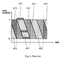
- Another method is to use the dark sub-frame between two neighboring color sub-frames as shown in FIG. 6 . Due to the use of the dark sub-frame, the total number of sub-frames per frame period increases twice compared to the previously described color sequential imaging methods shown in FIG. 4 . As shown in FIG. 6 , the red 401 , green 402 , and blue 403 backlights are turned on during two successive sub-frame periods. However, during these two successive sub-frame periods, there is one image sub-frame and one dark sub-frame. Using the red backlight 401 as an example, when the scan driver selects from the first row to the last row, an image sub-frame is inserted following the timing line 613 of row scanning 411 .
- FIG. 7 a shows the basic concept of LCD driving based on dual TFTs 710 in one sub-pixel.
- Each of these two TFTs has its own function: one functions as a memory part to store the image data and the other as an imaging part to control the director orientation of the liquid crystal layer 720 by using the data stored in the memory capacitor 708 .
- the data line 703 of the first TFT 701 is connected to the data driver 240 , as shown in FIG. 7B .
- the gate line 704 of the first TFT 701 is connected to the scan driver 250 .
- the drain 706 of the first TFT 701 is connected to the source of the second TFT 702 which is also connected to the first storage capacitor 707 .
- FIG. 7 b shows the electrodes connection between sub-pixels and drivers. Because each sub-pixel has two gate input lines G and VS, there are two lines in each sub-pixel which are connected to the scan driver.
- the timing chart of the color sequential LCD driving based on the dual TFT method is shown in FIG. 8 .
- the image data of red, green, and blue sub-frame are transferred to the frame buffer memory.
- data in the frame buffer are transferred to the second capacitor in the sub-pixels at time points of 801 , 802 , and 803 , as shown in FIG. 8 .
- Color of the backlight is changed synchronously with the time of triggering the second TFTs.
- the next sub-frame's image data are transferred to the frame buffer memory.
- the advantage of this method is it doesn't need dark sub-frames. Therefore, it doesn't lose energy of light.
- the first objective of this invention is to provide apparatus, methods, system and devices for a transflective LCD with a pixel structure including at least three reflective sub-pixels and one transmissive sub-pixel.
- the second objective of this invention is to provide apparatus, methods, system and devices for improved color reproduction capacity of the transflective LCD for both transmissive and reflective images by using color filters for the reflective sub-pixels to optimize the color filter property for the reflective images.
- a third objective of the present invention is to provide apparatus, methods, system and devices for maximizing the color purity of the transmissive image using a backlight which can switch the illumination colors sequentially.
- the fourth objective of the present invention is to provide apparatus, methods, system and devices that use the same electro-optic responses in both reflective and transflective modes in the transflective LCD without increasing the complexity of fabrication processes.
- a fifth objective of the present invention is to provide apparatus, methods, system and devices for driving the reflective sub-pixels and the transmissive sub-pixel with independent TFTs so that their electro-optic curves overlap by using a double TFT driving concept.
- a sixth objective of this invention is to provide apparatus, methods, system and devices for reducing the manufacturing cost of transflective LCD by eliminating complicated fabrication processes such as double cell gap, double domain alignment, and patterned retardation film.
- a seventh objective of the present invention is to provide apparatus, methods, system and devices for reducing the manufacturing cost of transflective LCD by eliminating the use of the dual thickness color filter for the optimization of the color purity for both transmissive and reflective mode images to simplify the fabrication process and increase the manufacturing yield.
- An eighth objective of the present invention is to provide apparatus, methods, system and devices for producing a brighter image in comparison to the image of prior art transflective LCDs.
- the transflective liquid crystal display includes a top and a bottom substrate having a liquid crystal layer sandwiched therebetween and plural pixels, each including at least three reflective sub-pixels for displaying a reflective image, wherein each one of the at least three reflective sub-pixels having a reflective layer on an inner surface of the bottom substrate to reflect an incident light back to a viewer, and a transmissive sub-pixel for displaying a transmissive image.
- At least one electronic circuit is used for driving the at least three reflective sub-pixels and the transmissive sub-pixel of each one of the plural pixels and a backlight below the transmissive sub-pixels for producing a transmissive image and a timing control unit connected with the at least one electronic circuit converts and distributes an incoming video data to the plural pixels and controlling the backlight to synchronize the reflective and transmissive display images.
- Each one of the plural pixels further includes at least three different color filter layers located on one of the top and the bottom substrate of the at least three reflective sub-pixels, respectively, for displaying a reflective color image and at least three different color light sources below the transmissive sub-pixel are used to sequentially transmit a color transmissive image for each of the at least three different colors.
- the at least one electronic circuit includes plural first and second scan electrodes, and plural first and second data electrodes, wherein one of the plural first scan electrodes and one of the plural first data electrode connect each one of the at least three reflective sub-pixels to the at least one electronic circuit and one of the plural second scan electrodes and one of the plural second data electrodes connect each one of the transmissive sub-pixel to the at least one electronic circuit.
- FIG. 1 shows a pixel of a prior art transflective liquid crystal display.
- FIG. 2 a is a schematic of the pixel electronic circuit having a single switch device.
- FIG. 2 b is a schematic showing the electrode connection between the pixel electronics in FIG. 2 a and the driver electronic circuits.
- FIG. 3 is a timing diagram of the prior art LCD operation.
- FIG. 4 is a timing diagram of the color sequential LCD under the ideal backlight operation.
- FIG. 5 is a timing diagram showing the color sequential LCD under the pulse type blinking backlight operation.
- FIG. 6 is a timing diagram showing the color sequential LCD under the blinking type backlight operation using a dark sub-frame between two primary color sub-frames.
- FIG. 7 a is a schematic showing the pixel electronics having dual switch devices in each sub-pixel.
- FIG. 7 b is a schematic showing the electrode connection between the pixel electronics shown in FIG. 7 a and the driver electronic circuits.
- FIG. 8 is a timing diagram of the color sequential LCD with dual switches in each sub-pixel under the blinking type backlight operation.
- FIG. 9 shows the schematic pixel layout and structure according present invention showing the plural sub-pixels.
- FIG. 10 a shows an example of the location of the pixel electronics in the pixel structure of FIG. 9 according to the present invention.
- FIG. 10 b shows an alternative location of the pixel electronics in the pixel structure shown in FIG. 9 according to the present invention.
- FIG. 11 is a schematic diagram showing yet another alternative electrode connection between the pixel electronics and the driver electronic circuits.
- FIG. 12 is a timing diagram showing the operation of the reflective sub-pixels and the transmissive sub-pixel of the transflective LCD shown in FIG. 11 .
- FIG. 13 is a timing diagram showing another example of the operation of the reflective sub-pixels and the transmissive sub-pixel of the transflective LCD shown in FIG. 11 .
- FIG. 14 is a schematic diagram showing an alternative electrode connection between the pixel electronics and the driver electronic circuits.
- FIG. 15 is a timing diagram showing the operation of the reflective sub-pixels and the transmissive sub-pixel of the transflective LCD shown in FIG. 14 .
- FIG. 16 is a timing diagram showing another example of the operation of the reflective sub-pixels and the transmissive sub-pixel of the transflective LCD shown in FIG. 14
- FIG. 17 is a schematic diagram showing an example of the electrode connection between the pixel electronics and the driver electronic circuits.
- FIG. 18 is a timing diagram showing an example of the operation of the reflective sub-pixels and the transmissive sub-pixel of the transflective LCD shown in FIG. 17 .
- the apparatus, methods, system and devices of the present invention provide a transflective liquid crystal display having a pixel structure including at least three sub-pixels for the reflective part and one sub-pixel for the transmissive part.
- the sub-pixel for the reflective part has a reflective mirror and a color filter for showing a color image by reflecting an ambient light.
- a sequentially switched color light from a backlit unit device is used and the transmissive color image is drawn using a series of primary color images.
- the reflective sub-pixels and the transmissive sub-pixel are independently switched by switching devices such as thin film transistors.
- both transmissive display mode and reflective display mode can overlap with each other very well.
- the switching devices and related peripheral electronics for both reflective and transmissive sub-pixels are located under the reflectors of the reflective sub-pixels on the bottom substrate. This electronic structure using a single transmissive sub-pixel configuration improves the aperture sizes of both reflective and transmissive sub-pixels compare to prior art. As a result, brighter image for both reflective and transmissive modes is produced.
- FIG. 9 shows a schematic structure and pixel layout of a transflective liquid crystal display of the present invention.
- each pixel 910 includes three reflective sub-pixels 901 , 902 , and 903 for displaying a reflective image and one transmissive sub-pixel 904 for displaying a transmissive image.
- Each reflective sub-pixel has a reflective mirror located on the inner surface of the bottom substrate to reflect the incident light back to the viewer.
- the reflective mode uses at least three primary color sub-pixels which have color filter layers located either on the bottom substrate or on the top substrate of the LCD.
- the three sub-pixels 901 , 902 , and 903 correspond to three primary color sub-pixels which are used to display a color reflective image.
- one transmissive sub-pixel 904 is used. This transmissive sub-pixel 904 transmits the light from a backlight source which is behind the LCD panel.
- a full color transmissive image in the transmissive sub-pixel 904 at least three different primary color lights transmit the transmissive sub-pixel 904 sequentially during one frame period, with one primary color light in each sub-frame of the frame period.
- the frame frequency is high enough, typically greater than approximately 30 frame/second, the viewer see a full color image.
- the method for displaying the transmissive color image is referred to as a color sequential imaging method.
- each of those sub-pixels 901 , 902 , 903 , and 904 is driven by an independent electronic switch comprising at least one thin film transistor and at least one capacitor.
- FIG. 10 a shows the location of sub-pixel electronic circuits in the present invention according to the first embodiment.
- the first reflective sub-pixel 901 has an electronic circuit 1011
- the second reflective sub-pixel 902 is driven by with electronic circuit 1012
- the third reflective sub-pixel 903 is driven by electronic circuit 1013
- the transmissive sub-pixel 904 is driven by electronic circuit 1014 as well.
- Each sub-pixel's electronic circuit is within the region of the corresponding sub-pixel.
- each sub-pixel has an opaque reflective mirror and the electronic circuits are located under the reflective mirror.
- the electronic circuits themselves do not affect the aperture ratio of the reflective sub-pixel, yielding a large aperture size and high light utilization efficiency.
- the transmissive sub-pixel the electronic circuits occupy a portion of the sub-pixel area which blocks part of the backlight. As a result, the aperture size is reduced and the brightness of image decreases.
- FIG. 10B shows the second embodiment of the location of sub-pixel electronic circuits in the present invention.
- the sub-pixel electronic circuits 1022 is also located under the reflectors of the reflective sub-pixels 901 , 902 , and 903 .
- the aperture ratio of all sub-pixels is maximized.
- the pixel structure of the present invention shown in FIG. 10 b increases the size of all sub-pixels.
- each pixel is divided into three different primary color sub-pixels. And the size of each sub-pixel equals to each other.
- Each sub-pixel has a discontinuous reflector film so that some part of the sub-pixel is transparent and the other part of the sub-pixel is opaque. The transparent part allows the backlight pass through it while the opaque part serves as the reflector to reflect the incident ambient light back to the viewers' eyes.
- each one of the three sub-pixels has an area ratio of the transmissive part to the reflective part of approximately 6:4. Therefore, area size of the transmissive part of each sub-pixel occupies approximately 20 percent of one entire pixel size, and the area size of the reflective part of each sub-pixel occupies about 13 percent of one entire pixel size.
- one pixel is divided into four equal sized sub-pixels, three reflective sub-pixels and one transmissive sub-pixel.
- the area size of each sub-pixel is approximately 25 percent of one entire pixel size.
- the area size of the transmissive sub-pixel increases 25 percent while the area size of the reflective sub-pixels increases 92 percent. As a result, the display has brighter image or can have lower power consumption in comparison with the conventional transflective LCDs.
- FIG. 11 shows the third embodiment of the present invention based on the pixel structure shown in FIG. 9 .
- one pixel 1101 has three reflective sub-pixels 1102 and one transmissive sub-pixel 1103 .
- the reflective sub-pixels 1102 are driven by the scan driver 1150 and the data driver 1140
- the transmissive sub-pixels 1103 is driven by the scan drivers 1151 and the data drivers 1141 .
- both reflective sub-pixels 1102 and transmissive sub-pixels 1103 are driven by a single-switch based electronic circuit 1110 .
- the video data is converted by a timing control unit 1120 and is distributed to the data drivers 1140 and 1141 and scan drivers 1150 and 1151 for the reflective and transmissive sub-pixels, respectively.
- the timing control unit 1120 also controls the backlight 1130 to synchronize the display of the reflective and transmissive color images.
- FIG. 12 shows an example of the operation timing diagram of the transflective LCD shown in FIG. 11 .
- the top graph 1210 is the timing diagram for displaying the reflective image and the bottom graph 1220 shows the timing diagram for displaying the transmissive image.
- the bottom graph 1220 shows the timing diagram for displaying the transmissive image.
- reflective sub-pixels are scanned by the scan driver 1150 and the first and the second frame images are drawn, respectively.
- the transmissive sub-pixels 904 are scanned six times along the timing lines 1231 , 1241 , 1232 , 1242 , 1233 , and 1243 , during which the three timing lines 1231 , 1232 , and 1233 are for the three primary color sub-frames 1221 , 1222 , and 1223 and the three timing lines 1241 , 1242 , and 1243 are for the three dark sub-frames.
- the transmissive data driver transfers the color image data to the transmissive sub-pixels, while during the three timing lines 1241 , 1242 , and 1243 , the transmissive data driver transfers the dark image data to the transmissive sub-pixels.
- the color sub-frame and the dark sub-frame are interleaved within the six sub-frames period.
- the first sub-frame scanning 1231 of the transmissive mode coincides with the frame scanning 1221 of the reflective mode.
- the first primary color of the backlight is activated between the time point when the first row of the transmissive sub-pixels are scanned at the first sub-frame scanning and the time point when the first row of the transmissive sub-pixels are scanned at the third sub-frame scanning.
- the second primary color of the backlight is activated between the time point when the first row of the transmissive sub-pixels are scanned at the third sub-frame scanning and the time point when the first row of the transmissive sub-pixels are scanned at the fifth sub-frame scanning
- the third primary color of the backlight is activated between the time point when the first row of the transmissive sub-pixels are scanned at the fifth sub-frame scanning and the time point when the first row of the transmissive sub-pixels are scanned at the first sub-frame scanning for the next frame. Therefore, the backlight is looked to switch its color on entire lighting area at a moment.
- dark image data are transferred from the data driver to the entire transmissive sub-pixels following the second, fourth, and sixth sub-frame scanning.
- FIG. 13 shows the second example of the operation timing diagram of the transflective LCD in the third embodiment of the present invention as shown in FIG. 11 .
- the top graph 1310 is the timing diagram for displaying the reflective image and the bottom graph 1320 is for displaying the transmissive image.
- reflective sub-pixels are scanned by the scan driver 1150 and the first and the second frame images are drawn, respectively.
- the transmissive sub-pixels 904 are scanned three times along the timing lines 1331 , 1332 , and 1333 .
- the primary color backlight is activated between the time point when the last row of the transmissive sub-pixels are scanned for the first sub-frame scanning and the time point when the first row of the transmissive sub-pixels are scanned for the second sub-frame.
- the second primary color backlight is activated between the time point when the last row of the transmissive sub-pixels are scanned for the second sub-frame scanning and the time point when the first row of the transmissive sub-pixels are scanned for the third sub-frame scanning
- the third primary color backlight is activated between the time point when the last row of the transmissive sub-pixels are scanned for the third sub-frame scanning and the time point when the first row of the transmissive sub-pixels are scanned for the first sub-frame scanning of the next frame imaging.
- the corresponding color sub-frame images are shown during the time period of 1321 , 1322 , and 1323 in the transmissive display mode. In this case, the image of whole area is drawn at a moment although the transmissive image data are transferred to the transmissive sub-pixels row by row.
- FIG. 14 shows an alternative configuration of the transflective LCD in the present invention.
- each pixel 1401 comprises three reflective sub-pixels 1402 and one transmissive sub-pixel 1403 .
- the reflective sub-pixels 1402 are driven by a single electronic circuit 1410
- the transmissive sub-pixel 1403 is driven by dual-switch based electronic circuits 1411 as explained in the description of the configuration shown in FIG. 7A .
- the reflective sub-pixels 1402 are connected with the scan driver 1450 and the data driver 1440 .
- the transmissive sub-pixels 1403 are connected with the scan driver 1451 and the data driver 1441 .
- Timing control unit 1420 also synchronizes the backlight 1430 operation with the transmissive sub-pixel 1403 operation. In addition, it synchronizes the reflective image displayed by the reflective sub-pixels 1402 with the transmissive image displayed by the transmissive sub-pixels 1403 .
- FIG. 15 shows the first example of the operation timing diagram of the transflective LCD in the fourth embodiment of the present invention as shown in FIG. 14 .
- the top graph 1510 is the timing diagram for displaying the reflective image and the bottom graph 1520 shows the timing diagram for displaying the transmissive image.
- One frame scanning 1511 of the reflective mode coincides with the first sub-frame scanning 1531 of the transmissive mode.
- Reflective mode holds the image data for three sub-frame periods of the transmissive mode.
- the transmissive mode draws the whole area of the image at one time by using the frame buffer method previously described in regard to the configuration shown in FIG. 8 .
- each primary color is activated during the time period between the time point when the first row of the transmissive sub-pixels are scanned for one sub-frame and the time point when the first row of the transmissive sub-pixels are scanned for the following sub-frame. Because of the difference of imaging method between reflective and transmissive mode, image holding times of the transmissive mode in the first and the third sub-frames are not synchronized with that of the reflective mode.
- FIG. 16 shows another example of the operation timing diagram of the transflective LCD shown in FIG. 14 .
- the top graph 1610 is the timing diagram for displaying the reflective image and the bottom graph 1620 is for displaying the transmissive image.
- one dark sub-frame 1624 is introduced after the third sub-frame 1623 .
- the data of the dark sub-frame 1624 are transferred to the frame buffer memory together with the scanning 1633 , and further are sent to the imaging part, liquid crystal layer, at the time 1604 .
- the backlight is turned-off during the dark sub-frame period.
- the first and last sub-frames in the transmissive mode match with the beginning and end of one frame in the reflective mode.
- FIG. 17 is a schematic diagram showing another configuration of the transflective LCD according to the present invention.
- each pixel 1701 comprises three reflective sub-pixels 1702 and one transmissive sub-pixel 1703 , however, both reflective sub-pixels 1702 and transmissive sub-pixels 1703 are driven by dual-switch based pixel electronic circuits 1710 as previously described in regard to the configuration shown in FIG. 7A .
- the reflective sub-pixels 1702 are connected with the scan driver 1750 and the data driver 1740 while the transmissive sub-pixels 1703 are connected with the scan driver 1751 and the data driver 1741 .
- the video data are converted by a timing control unit 1720 and is further distributed to all data drivers 1740 and 1741 and scan drivers 1750 and 1751 .
- Timing control unit 1720 also synchronizes the backlight 1730 operation with the transmissive sub-pixel 1703 operation. In addition, it synchronizes the reflective image displayed by the reflective sub-pixels 1702 with the transmissive image displayed by the transmissive sub-pixels 1703 .
- FIG. 18 shows the operation timing diagram of the transflective LCD configuration shown in FIG. 17 .
- the top graph 1810 is the timing diagram for displaying the reflective image and the bottom graph 1820 is for displaying the transmissive image.
- the first frame scanning 1811 of the reflective mode coincides with the first sub-frame scanning 1831 of the first frame of transmissive mode.
- data in the frame buffer of transmissive and reflective sub-pixels are transferred to the second capacitor in the sub-pixels at the same time point 1801 and 1841 .
- the reflective image is hold for three sub-frames time of the transmissive mode and the transmissive image of each primary color is hold for one sub-frame time of the transmissive mode.
- image data for the second frame image of the reflective mode and data for the first sub-frame image of the second fame of the transmissive mode are transferred to the frame buffer memory of both reflective and transmissive sub-pixels along the timing line of reflective mode scanning 1812 and the timing line of transmissive mode scanning 1834 .
- data for reflective image in the frame buffer memory are transferred to the second capacitor in the reflective sub-pixels by triggering the second TFT's gate at the time point 1842 .
- data for transmissive image in the frame buffer memory are transferred to the second capacitor in the transmissive sub-pixels at the time point 1804 .
- Timing control unit 1720 synchronizes the time point 1842 with the time point 1804 . Due to this timing synchronization, the image frame of the transmissive mode can match perfectly with the image frame of the reflective mode without dark sub-frames used in the fourth embodiment as shown in FIG. 16 . To synchronize the backlight operation with sub-frames of transmissive mode, each primary color is activated as the same manner described in FIG. 15 .
Abstract
Description
| 100 | prior art pixel structure |
| 101 | red sub-pixel |
| 102 | green sub-pixel |
| 103 | blue sub-pixel |
| 111 | red transmission region |
| 112 | green transmission region |
| 113 | blue transmission region |
| 201 | source terminal |
| 202 | gate terminal |
| 203 | drain terminal |
| 210 | pixel electronic circuit |
| 211 | thin film transistor |
| 212 | capacitor |
| 220 | liquid crystal layer |
| 230 | vertical sync signal |
| 240 | data driver |
| 250 | scan gate driver |
| 311 | first timing line |
| 312 | second timing line |
| 313 | third timing line |
| 314 | fourth timing line |
| 320 | image data |
| 401 | red area |
| 402 | green area |
| 403 | blue area |
| 411 | red timing line |
| 412 | green timing line |
| 413 | blue timing line |
| 520 | image data |
| 611 | next scanning line |
| 613 | timing line |
| 701 | first thin film transistor |
| 702 | second thin film transistor |
| 703 | data line |
| 704 | first gate line |
| 705 | second gate line |
| 706 | TFT drain |
| 707 | first capacitor |
| 708 | memory capacitor |
| 710 | pixel electronic circuit |
| 720 | liquid crystal layer |
| 801 | time one |
| 802 | time two |
| 803 | time three |
| 901 | first reflective sub-pixel |
| 902 | second reflective sub-pixel |
| 903 | third reflective sub-pixel |
| 904 | transmissive sub-pixel |
| 910 | transflective pixel |
| 1011 | first reflective pixel electronics |
| 1012 | second reflective pixel electronics |
| 1013 | third reflective pixel electronics |
| 1022 | transmissive pixel electronic circuit |
| 1101 | pixel |
| 1102 | reflective sub-pixels |
| 1103 | transmissive sub-pixel |
| 1110 | pixel electronic circuit |
| 1120 | timing control unit |
| 1130 | backlight |
| 1140 | reflective data driver |
| 1141 | transmissive image data drivers |
| 1150 | reflective scan driver |
| 1151 | transmissive scan drivers |
| 1210 | reflective timing graph |
| 1211 | timing line |
| 1212 | timing line |
| 1220 | transmissive timing graph |
| 1221 | color sub-frame |
| 1222 | color sub-frame |
| 1223 | color sub-frame |
| 1231 | color sub-frame timing |
| 1232 | color sub-frame timing |
| 1233 | color sub-frame timing |
| 1241 | dark sub-frame timing |
| 1242 | dark sub-frame timing |
| 1243 | dark sub-frame timing |
| 1310 | reflective graph |
| 1311 | reflective scan time |
| 1312 | reflective scan time |
| 1320 | transmissive graph |
| 1321 | color sub-frame |
| 1322 | color sub-frame |
| 1323 | color sub-frame |
| 1331 | transmissive scan time |
| 1332 | transmissive scan time |
| 1333 | transmissive scan time |
| 1401 | pixel |
| 1402 | reflective sub-pixels |
| 1403 | transmissive sub-pixel |
| 1410 | reflective pixel electronic circuit |
| 1411 | transmissive pixel electronic circuit |
| 1420 | timing control unit |
| 1430 | backlight |
| 1440 | reflective data driver |
| 1441 | transmissive image data driver |
| 1450 | reflective scan driver |
| 1451 | transmissive scan driver |
| 1510 | reflective timing graph |
| 1511 | reflective frame scanning |
| 1520 | transmissive timing graph |
| 1531 | first transmissive sub-frame scanning |
| 1604 | time |
| 1610 | reflective timing diagram |
| 1620 | transmissive image timing |
| 1621 | first color sub-frame |
| 1622 | second color sub-frame |
| 1623 | third color sub-frame |
| 1624 | dark sub-frame |
| 1633 | scanning |
| 1701 | pixel |
| 1702 | reflective sub-pixels |
| 1703 | transmissive sub-pixel |
| 1710 | pixel electronic circuit |
| 1720 | timing control unit |
| 1730 | backlight |
| 1740 | first data driver |
| 1741 | second data driver |
| 1750 | first scan driver |
| 1751 | second scan driver |
| 1801 | time |
| 1804 | time |
| 1810 | reflective timing graph |
| 1811 | first reflective frame scan |
| 1812 | reflective mode scan |
| 1820 | transmissive timing graph |
| 1831 | first transmissive sub-frame scan |
| 1834 | transmissive mode scan |
| 1842 | time point |
Claims (32)
Priority Applications (4)
| Application Number | Priority Date | Filing Date | Title |
|---|---|---|---|
| US11/404,539 US7746294B2 (en) | 2006-04-14 | 2006-04-14 | Transflective liquid crystal display |
| TW096112998A TWI365328B (en) | 2006-04-14 | 2007-04-13 | Transflective liquid crystal display |
| CN2007100960858A CN101055359B (en) | 2006-04-14 | 2007-04-13 | Semi-penetration/ reflection liquid crystal display and its production method |
| US12/766,357 US8279140B2 (en) | 2006-04-14 | 2010-04-23 | Transflective liquid crystal display |
Applications Claiming Priority (1)
| Application Number | Priority Date | Filing Date | Title |
|---|---|---|---|
| US11/404,539 US7746294B2 (en) | 2006-04-14 | 2006-04-14 | Transflective liquid crystal display |
Related Child Applications (1)
| Application Number | Title | Priority Date | Filing Date |
|---|---|---|---|
| US12/766,357 Division US8279140B2 (en) | 2006-04-14 | 2010-04-23 | Transflective liquid crystal display |
Publications (2)
| Publication Number | Publication Date |
|---|---|
| US20070242014A1 US20070242014A1 (en) | 2007-10-18 |
| US7746294B2 true US7746294B2 (en) | 2010-06-29 |
Family
ID=38604388
Family Applications (2)
| Application Number | Title | Priority Date | Filing Date |
|---|---|---|---|
| US11/404,539 Expired - Fee Related US7746294B2 (en) | 2006-04-14 | 2006-04-14 | Transflective liquid crystal display |
| US12/766,357 Expired - Fee Related US8279140B2 (en) | 2006-04-14 | 2010-04-23 | Transflective liquid crystal display |
Family Applications After (1)
| Application Number | Title | Priority Date | Filing Date |
|---|---|---|---|
| US12/766,357 Expired - Fee Related US8279140B2 (en) | 2006-04-14 | 2010-04-23 | Transflective liquid crystal display |
Country Status (3)
| Country | Link |
|---|---|
| US (2) | US7746294B2 (en) |
| CN (1) | CN101055359B (en) |
| TW (1) | TWI365328B (en) |
Cited By (3)
| Publication number | Priority date | Publication date | Assignee | Title |
|---|---|---|---|---|
| US20080100566A1 (en) * | 2006-10-25 | 2008-05-01 | Seiko Epson Corporation | Electrooptic device and electronic apparatus |
| US20080129673A1 (en) * | 2006-12-04 | 2008-06-05 | Hee-Seop Kim | Display device and method of driving the same |
| US20100026613A1 (en) * | 2006-05-30 | 2010-02-04 | Thomson Licensing | Methods for Sequential Color Display by Modulation of Pulses |
Families Citing this family (20)
| Publication number | Priority date | Publication date | Assignee | Title |
|---|---|---|---|---|
| KR20060114921A (en) * | 2005-05-03 | 2006-11-08 | 삼성전자주식회사 | Liquid crystal display |
| GB0512829D0 (en) * | 2005-06-23 | 2005-08-03 | Magink Display Technologies | Video drive scheme for a cholesteric liquid crystal display device |
| JP4197000B2 (en) * | 2005-07-07 | 2008-12-17 | エプソンイメージングデバイス株式会社 | Electro-optical device and electronic apparatus |
| JP2008052259A (en) * | 2006-07-26 | 2008-03-06 | Toshiba Matsushita Display Technology Co Ltd | Liquid crystal display device |
| TWI336805B (en) * | 2006-12-07 | 2011-02-01 | Chimei Innolux Corp | Liquid crystal display device and driving method thereof |
| US8089590B2 (en) * | 2007-08-06 | 2012-01-03 | Chimei Innolux Corporation | Transflective liquid crystal display |
| TW201017273A (en) * | 2008-07-16 | 2010-05-01 | Pixel Qi Corp | Transflective display |
| WO2010014598A2 (en) * | 2008-07-28 | 2010-02-04 | Pixel Qi Corporation | Triple mode liquid crystal display |
| US8670004B2 (en) * | 2009-03-16 | 2014-03-11 | Pixel Qi Corporation | Driving liquid crystal displays |
| CN102844806B (en) * | 2009-12-28 | 2016-01-20 | 株式会社半导体能源研究所 | Liquid crystal indicator and electronic equipment |
| TWI404014B (en) * | 2010-05-25 | 2013-08-01 | Au Optronics Corp | Display panel and driving circuit thereof |
| TWI582744B (en) * | 2014-05-08 | 2017-05-11 | 友達光電股份有限公司 | Operation method of transflective display apparatus and transflective display apparatus |
| US20150332641A1 (en) * | 2014-05-13 | 2015-11-19 | Innolux Corporation | Transflective panel device |
| KR20160112143A (en) | 2015-03-18 | 2016-09-28 | 삼성전자주식회사 | Electronic device and method for updating screen of display panel thereof |
| CN104992686A (en) * | 2015-07-21 | 2015-10-21 | 京东方科技集团股份有限公司 | Display panel and driving method and driving device thereof |
| CN105093600B (en) * | 2015-08-17 | 2018-11-06 | 京东方科技集团股份有限公司 | A kind of display panel and display device |
| CN105185812B (en) * | 2015-09-08 | 2017-12-22 | 京东方科技集团股份有限公司 | OLED pixel structure, display base plate and display device |
| US10290269B2 (en) * | 2016-02-29 | 2019-05-14 | Motorola Mobility Llc | Hybrid liquid crystal display |
| WO2018073706A1 (en) * | 2016-10-21 | 2018-04-26 | Semiconductor Energy Laboratory Co., Ltd. | Display device and operating method thereof |
| CN108877699B (en) * | 2017-05-08 | 2021-02-09 | 北京小米移动软件有限公司 | Display panel |
Citations (14)
| Publication number | Priority date | Publication date | Assignee | Title |
|---|---|---|---|---|
| US4040727A (en) | 1975-09-10 | 1977-08-09 | Rockwell International Corporation | Transflector |
| US4090219A (en) | 1974-12-09 | 1978-05-16 | Hughes Aircraft Company | Liquid crystal sequential color display |
| US4093356A (en) | 1977-02-14 | 1978-06-06 | General Electric Company | Transflective liquid crystal display |
| US4870396A (en) | 1987-08-27 | 1989-09-26 | Hughes Aircraft Company | AC activated liquid crystal display cell employing dual switching devices |
| US6281952B1 (en) | 1997-12-26 | 2001-08-28 | Sharp Kabushiki Kaisha | Liquid crystal display |
| US20030151580A1 (en) * | 2002-02-11 | 2003-08-14 | Yao-Dong Ma | Motion video cholesteric displays |
| US20060012552A1 (en) * | 2004-07-16 | 2006-01-19 | Au Optronics Corp. | Liquid crystal display with image flicker and shadow elimination functions applied when power-off and an operation method of the same |
| US20060087486A1 (en) * | 2004-10-21 | 2006-04-27 | I-Shu Lee | Control module and method for controlling backlight module of lcd |
| US20070076145A1 (en) * | 2005-10-04 | 2007-04-05 | Toppoly Optoelectronics Corp. | Display panel having a reflective layer therein |
| US20080055519A1 (en) * | 2004-10-08 | 2008-03-06 | Koninklijke Philips Electronics, N.V. | Transflective Liquid Crystal Display Device |
| US20080252588A1 (en) * | 2005-02-25 | 2008-10-16 | Tpo Hong Kong Holding Limited | Column Electrode Driving Circuit and Display Device Using It |
| US7499116B2 (en) * | 2006-04-11 | 2009-03-03 | Tpo Displays Corp. | Systems for displaying images having micro-reflective transmission liquid crystal display with particular storage capacitor arrangement |
| US7499128B2 (en) * | 2004-04-27 | 2009-03-03 | Au Optronics Corp. | Liquid crystal panel with improved chromaticity and brightness |
| US7564530B2 (en) * | 2005-12-29 | 2009-07-21 | Au Optronics Corporation | Sub-pixel structure in transflective color liquid crystal display |
Family Cites Families (5)
| Publication number | Priority date | Publication date | Assignee | Title |
|---|---|---|---|---|
| KR100439354B1 (en) * | 2002-07-08 | 2004-07-07 | 엘지.필립스 엘시디 주식회사 | Transflective LCD |
| EP1529239B1 (en) * | 2002-08-02 | 2005-12-14 | Koninklijke Philips Electronics N.V. | Transflective liquid crystal display device |
| CN100395590C (en) * | 2004-03-08 | 2008-06-18 | 奇美电子股份有限公司 | Semi-transmissive and reflective type liquid crystal display and dot structure thereof |
| JP4123194B2 (en) * | 2004-06-15 | 2008-07-23 | セイコーエプソン株式会社 | Liquid crystal display device and electronic device |
| JP4642785B2 (en) * | 2005-01-12 | 2011-03-02 | シャープ株式会社 | Liquid crystal display device |
-
2006
- 2006-04-14 US US11/404,539 patent/US7746294B2/en not_active Expired - Fee Related
-
2007
- 2007-04-13 CN CN2007100960858A patent/CN101055359B/en not_active Expired - Fee Related
- 2007-04-13 TW TW096112998A patent/TWI365328B/en not_active IP Right Cessation
-
2010
- 2010-04-23 US US12/766,357 patent/US8279140B2/en not_active Expired - Fee Related
Patent Citations (14)
| Publication number | Priority date | Publication date | Assignee | Title |
|---|---|---|---|---|
| US4090219A (en) | 1974-12-09 | 1978-05-16 | Hughes Aircraft Company | Liquid crystal sequential color display |
| US4040727A (en) | 1975-09-10 | 1977-08-09 | Rockwell International Corporation | Transflector |
| US4093356A (en) | 1977-02-14 | 1978-06-06 | General Electric Company | Transflective liquid crystal display |
| US4870396A (en) | 1987-08-27 | 1989-09-26 | Hughes Aircraft Company | AC activated liquid crystal display cell employing dual switching devices |
| US6281952B1 (en) | 1997-12-26 | 2001-08-28 | Sharp Kabushiki Kaisha | Liquid crystal display |
| US20030151580A1 (en) * | 2002-02-11 | 2003-08-14 | Yao-Dong Ma | Motion video cholesteric displays |
| US7499128B2 (en) * | 2004-04-27 | 2009-03-03 | Au Optronics Corp. | Liquid crystal panel with improved chromaticity and brightness |
| US20060012552A1 (en) * | 2004-07-16 | 2006-01-19 | Au Optronics Corp. | Liquid crystal display with image flicker and shadow elimination functions applied when power-off and an operation method of the same |
| US20080055519A1 (en) * | 2004-10-08 | 2008-03-06 | Koninklijke Philips Electronics, N.V. | Transflective Liquid Crystal Display Device |
| US20060087486A1 (en) * | 2004-10-21 | 2006-04-27 | I-Shu Lee | Control module and method for controlling backlight module of lcd |
| US20080252588A1 (en) * | 2005-02-25 | 2008-10-16 | Tpo Hong Kong Holding Limited | Column Electrode Driving Circuit and Display Device Using It |
| US20070076145A1 (en) * | 2005-10-04 | 2007-04-05 | Toppoly Optoelectronics Corp. | Display panel having a reflective layer therein |
| US7564530B2 (en) * | 2005-12-29 | 2009-07-21 | Au Optronics Corporation | Sub-pixel structure in transflective color liquid crystal display |
| US7499116B2 (en) * | 2006-04-11 | 2009-03-03 | Tpo Displays Corp. | Systems for displaying images having micro-reflective transmission liquid crystal display with particular storage capacitor arrangement |
Non-Patent Citations (2)
| Title |
|---|
| Fujimori, Kohichi, et al., 53.3: "New Color Filter Structures for Transflective TFT-LCD", Sharp Corporation., Display Technology Development Group, 2002, SID Digest International Symposium, p. 1382-1385. |
| Lee, Baek-woon, et al., "40.5L: Late-News Paper: TFT-LCD with RGBW Color System", Samsung Electronics Corp., in Proceeding of International Display Manufacturing Conference 2003, SID Digest, p. 212-215. |
Cited By (6)
| Publication number | Priority date | Publication date | Assignee | Title |
|---|---|---|---|---|
| US20100026613A1 (en) * | 2006-05-30 | 2010-02-04 | Thomson Licensing | Methods for Sequential Color Display by Modulation of Pulses |
| US8184133B2 (en) * | 2006-05-30 | 2012-05-22 | Thomson Licensing | Methods for sequential color display by modulation of pulses |
| US20080100566A1 (en) * | 2006-10-25 | 2008-05-01 | Seiko Epson Corporation | Electrooptic device and electronic apparatus |
| US7961171B2 (en) * | 2006-10-25 | 2011-06-14 | Seiko Epson Corporation | Electrooptic device and electronic apparatus |
| US20080129673A1 (en) * | 2006-12-04 | 2008-06-05 | Hee-Seop Kim | Display device and method of driving the same |
| US8427515B2 (en) * | 2006-12-04 | 2013-04-23 | Samusng Display Co., Ltd. | Display device and method of driving the same |
Also Published As
| Publication number | Publication date |
|---|---|
| TW200801700A (en) | 2008-01-01 |
| US20070242014A1 (en) | 2007-10-18 |
| CN101055359A (en) | 2007-10-17 |
| TWI365328B (en) | 2012-06-01 |
| CN101055359B (en) | 2010-05-26 |
| US20100201723A1 (en) | 2010-08-12 |
| US8279140B2 (en) | 2012-10-02 |
Similar Documents
| Publication | Publication Date | Title |
|---|---|---|
| US7746294B2 (en) | Transflective liquid crystal display | |
| JP3952362B2 (en) | Color video display method for time-division liquid crystal display device | |
| US7492345B2 (en) | Liquid crystal display for performing time divisional color display, method of driving the same backlight unit for liquid crystal display | |
| US8686932B2 (en) | Liquid crystal display device and method for driving the same | |
| US8587580B2 (en) | Liquid crystal display | |
| KR20040069958A (en) | Display device and display method | |
| KR20020096911A (en) | Liquid crystal display device | |
| JP2004191836A (en) | Display device and display method | |
| Lee et al. | Novel color-sequential transflective liquid crystal displays | |
| US20050030272A1 (en) | Electro-optical device and driving method thereof, projection-type display device, and electronic apparatus | |
| US7012598B2 (en) | Liquid crystal display device and method for operating the same | |
| US20080158141A1 (en) | Display method and display device | |
| US20130044273A1 (en) | Liquid crystal display device and method for controlling scanning backlight | |
| TW200529136A (en) | Display device, method of driving the same, and projection display device | |
| US7221353B2 (en) | Liquid crystal display device and method for operating the same | |
| WO2005088599A1 (en) | Full color video display using black-white display with tri-color light source | |
| JP2003316335A (en) | Liquid crystal display device and method for driving the same | |
| JP4453356B2 (en) | Liquid crystal display | |
| US20090207114A1 (en) | Liquid crystal display device | |
| JP2008261944A (en) | Liquid crystal display | |
| US20080013008A1 (en) | Liquid Crystal Driving Circuit and Liquid Crystal Display Device with the Same | |
| JP2007193124A (en) | Liquid crystal display device | |
| KR100685432B1 (en) | Liquid Crystal Display Device for having a common backlight unit used in LCD of FS-driving type or LCD of CF-driving type | |
| KR100983712B1 (en) | Unit of driving liquid crystal display | |
| JP2006195387A (en) | Electro-optical device and electronic equipment |
Legal Events
| Date | Code | Title | Description |
|---|---|---|---|
| AS | Assignment |
Owner name: UNIVERSITY OF CENTRAL FLORIDA RESEARCH FOUNDATION, Free format text: ASSIGNMENT OF ASSIGNORS INTEREST;ASSIGNORS:LEE, JU-HYUN;ZHU, XINYU;WU, SHIN-TSON;REEL/FRAME:017792/0071 Effective date: 20060411 Owner name: TOPPOLY OPTOELECTRONICS CORP., TAIWAN Free format text: ASSIGNMENT OF ASSIGNORS INTEREST;ASSIGNORS:LEE, JU-HYUN;ZHU, XINYU;WU, SHIN-TSON;REEL/FRAME:017792/0071 Effective date: 20060411 Owner name: TOPPOLY OPTOELECTRONICS CORP.,TAIWAN Free format text: ASSIGNMENT OF ASSIGNORS INTEREST;ASSIGNORS:LEE, JU-HYUN;ZHU, XINYU;WU, SHIN-TSON;REEL/FRAME:017792/0071 Effective date: 20060411 |
|
| STCF | Information on status: patent grant |
Free format text: PATENTED CASE |
|
| AS | Assignment |
Owner name: TPO DISPLAYS CORP., TAIWAN Free format text: CHANGE OF NAME;ASSIGNOR:TOPPOLY OPTOELECTRONICS CORP.;REEL/FRAME:025586/0195 Effective date: 20060605 |
|
| AS | Assignment |
Owner name: CHIMEI INNOLUX CORPORATION, TAIWAN Free format text: MERGER;ASSIGNOR:TPO DISPLAYS CORP.;REEL/FRAME:025918/0759 Effective date: 20100318 |
|
| REMI | Maintenance fee reminder mailed | ||
| AS | Assignment |
Owner name: INNOLUX CORPORATION, TAIWAN Free format text: CHANGE OF NAME;ASSIGNOR:CHIMEI INNOLUX CORPORATION;REEL/FRAME:032621/0718 Effective date: 20121219 |
|
| FPAY | Fee payment |
Year of fee payment: 4 |
|
| SULP | Surcharge for late payment | ||
| FEPP | Fee payment procedure |
Free format text: MAINTENANCE FEE REMINDER MAILED (ORIGINAL EVENT CODE: REM.) |
|
| LAPS | Lapse for failure to pay maintenance fees |
Free format text: PATENT EXPIRED FOR FAILURE TO PAY MAINTENANCE FEES (ORIGINAL EVENT CODE: EXP.); ENTITY STATUS OF PATENT OWNER: LARGE ENTITY |
|
| STCH | Information on status: patent discontinuation |
Free format text: PATENT EXPIRED DUE TO NONPAYMENT OF MAINTENANCE FEES UNDER 37 CFR 1.362 |
|
| FP | Lapsed due to failure to pay maintenance fee |
Effective date: 20220629 |