JP4453356B2 - Liquid crystal display - Google Patents
Liquid crystal display Download PDFInfo
- Publication number
- JP4453356B2 JP4453356B2 JP2003420352A JP2003420352A JP4453356B2 JP 4453356 B2 JP4453356 B2 JP 4453356B2 JP 2003420352 A JP2003420352 A JP 2003420352A JP 2003420352 A JP2003420352 A JP 2003420352A JP 4453356 B2 JP4453356 B2 JP 4453356B2
- Authority
- JP
- Japan
- Prior art keywords
- liquid crystal
- crystal display
- primary color
- substrate
- video signal
- Prior art date
- Legal status (The legal status is an assumption and is not a legal conclusion. Google has not performed a legal analysis and makes no representation as to the accuracy of the status listed.)
- Expired - Fee Related
Links
- 239000004973 liquid crystal related substance Substances 0.000 title claims description 72
- 239000000758 substrate Substances 0.000 claims description 27
- 239000003990 capacitor Substances 0.000 claims description 18
- 238000000034 method Methods 0.000 claims description 14
- 238000005286 illumination Methods 0.000 claims description 11
- 230000007704 transition Effects 0.000 claims description 7
- 230000001678 irradiating effect Effects 0.000 claims 1
- 210000002858 crystal cell Anatomy 0.000 description 10
- 239000003086 colorant Substances 0.000 description 6
- 238000010586 diagram Methods 0.000 description 4
- 230000003287 optical effect Effects 0.000 description 4
- 101100298998 Caenorhabditis elegans pbs-3 gene Proteins 0.000 description 3
- XUIMIQQOPSSXEZ-UHFFFAOYSA-N Silicon Chemical compound [Si] XUIMIQQOPSSXEZ-UHFFFAOYSA-N 0.000 description 3
- 229910052710 silicon Inorganic materials 0.000 description 3
- 239000010703 silicon Substances 0.000 description 3
- 230000001360 synchronised effect Effects 0.000 description 3
- 238000003780 insertion Methods 0.000 description 2
- 230000037431 insertion Effects 0.000 description 2
- 206010047571 Visual impairment Diseases 0.000 description 1
- 230000005540 biological transmission Effects 0.000 description 1
- 230000007423 decrease Effects 0.000 description 1
- 239000011159 matrix material Substances 0.000 description 1
- 230000010287 polarization Effects 0.000 description 1
- 238000009877 rendering Methods 0.000 description 1
- 210000001525 retina Anatomy 0.000 description 1
- 238000000926 separation method Methods 0.000 description 1
Images


Landscapes
- Liquid Crystal (AREA)
- Liquid Crystal Display Device Control (AREA)
- Control Of Indicators Other Than Cathode Ray Tubes (AREA)
Description
本発明は液晶表示装置に係り、特にベンド配向を有する液晶表示素子を用いてフィールドシーケンシャル方式カラー表示を実現する液晶表示装置に関する。 The invention relates to a liquid crystal display apparatus, a liquid crystal display apparatus to realize the field sequential type color display have use a liquid crystal display element having a particularly bend alignment.
動画像の表示やフィールドシーケンシャル表示に適した高速応答性を有する液晶表示素子として、OCB(Optically Compensated Birefringence)モードの液晶表示素子が知られている。この液晶表示素子では、2枚の基板間に挟まれた液晶層(液晶分子)の配向状態を、表示に適さない初期の配向状態であるスプレイ配向から、2枚の基板間に一定の電位差を与えて表示に適したベンド配向に転移させる必要がある。このため、かかる液晶表示素子をスプレイ配向からベンド配向へ短時間に確実に転移させる駆動方法が、従来より種々提案されている(例えば、特許文献1、2参照)。
An OCB (Optically Compensated Birefringence) mode liquid crystal display element is known as a liquid crystal display element having high-speed response suitable for moving image display and field sequential display. In this liquid crystal display element, the liquid crystal layer (liquid crystal molecule) sandwiched between two substrates is changed from a splay alignment, which is an initial alignment state unsuitable for display, to a constant potential difference between the two substrates. It is necessary to shift to a bend orientation suitable for display. For this reason, various driving methods for reliably transferring such a liquid crystal display element from splay alignment to bend alignment in a short time have been conventionally proposed (see, for example,
上記の特許文献1には、液晶層を挟む対向電極間の電位の変化点で画素トランジスタをオンにするゲート線電位を与えておいて、対向電極間の電位の変化による画素電極電位の変化を防止して、画素電極と対向電極の間に所定の電圧差を与えることにより、短時間でベンド配向に転移させる液晶表示素子の駆動方法が開示されている。
In the above-mentioned
また、上記の特許文献2には、液晶パネルの画素電極と対向電極の間に通常映像表示時よりも高い電位差を連続的に印加する期間を設けることにより、液晶層を短時間でベンド配向に転移させる液晶表示素子の駆動方法が開示されている。
Further, in
ところで、一般に、液晶表示装置のカラー化の手段として、1フレーム期間を3フィールドに分割して、各フィールド期間毎に赤色、緑色、青色の三原色の画像データで液晶パネルを切り替えていくと共に、これに同期させて液晶パネル面に照射する光源を、時系列的に三原色光である赤色光、緑色光、青色光で順次に切り替え、各原色光に対応した残像を人の網膜上で合成してカラー画像を得る、いわゆるフィールドシーケンシャル方式(面順次方式)の液晶表示装置が知られている。このフィールドシーケンシャル方式の液晶表示装置では、液晶表示素子の高速応答性が要求されるため、上記のOCBモードの液晶表示素子の駆動方法を適用して好適である。 By the way, in general, as a means for colorization of a liquid crystal display device, one frame period is divided into three fields, and the liquid crystal panel is switched by image data of three primary colors of red, green, and blue for each field period. The light source that illuminates the liquid crystal panel surface in synchronization with the three primary colors of red light, green light, and blue light is sequentially switched in time series, and afterimages corresponding to each primary color light are synthesized on the human retina. A so-called field sequential type (frame sequential type) liquid crystal display device for obtaining a color image is known. In this field sequential type liquid crystal display device, since the high-speed response of the liquid crystal display element is required, it is preferable to apply the above-described OCB mode liquid crystal display element driving method.
しかるに、上記の従来の液晶表示素子の駆動方法は、短時間でベンド配向に転移させることを目的として、いずれも通常の映像信号を駆動する場合よりも高い電位差を映像信号に印加する期間を設けるようにしているため、映像信号の供給ラインの他に配向状態転移用の電圧供給ラインが必要となり、また、信号の切替手段が必要となる。 However, in the above conventional liquid crystal display element driving methods, a period for applying a higher potential difference to the video signal than that for driving a normal video signal is provided for the purpose of transitioning to bend alignment in a short time. Therefore, in addition to the video signal supply line, a voltage supply line for alignment state transition is required, and a signal switching means is required.
また、従来のフィールドシーケンシャル方式の液晶表示装置では、3原色の画像をフィールド毎に切り替えて表示するようにしているため、あるフィールド期間では1つの原色しか表示できず、この結果、照明光の利用効率が最大でも1/3になり、表示が暗くなってしまうという問題がある。また、色バランスをとるために、赤色光、緑色光、青色光のうちで光強度の最も弱い原色光に他の2つの原色光の光強度を合わせるので、光の利用効率が悪くなる場合がある。更に、黒表示の挿入が映像信号によっては、うまく実現できないことがある。 Further, in the conventional field sequential type liquid crystal display device, since the three primary color images are switched and displayed for each field, only one primary color can be displayed in a certain field period. As a result, the use of illumination light is possible. There is a problem that the efficiency becomes 1/3 at the maximum and the display becomes dark. In addition, in order to balance the colors, the light intensity of the other two primary colors is matched with the primary color light having the weakest light intensity among red light, green light, and blue light. is there. Furthermore, insertion of black display may not be realized successfully depending on the video signal.
本発明は以上の点に鑑みなされたもので、光の利用率を向上し得るフィールドシーケンシャル方式の液晶表示装置を提供することを目的とする。 The present invention has been made in view of the above points, and an object thereof is to provide a field sequential type liquid crystal display device capable of improving the utilization factor of light .
更に、本発明の他の目的は、黒表示の挿入による動画性能の向上を図り得るフィールドシーケンシャル方式の液晶表示装置を提供することにある。 It is another object of the present invention to provide a field sequential type liquid crystal display device capable of improving moving image performance by inserting a black display.
上記の目的を達成するため、第1の発明は、少なくともトランジスタ及び画素電極が形成された第1の基板と、この第1の基板の対向面に共通電極が形成された第2の基板との間に液晶層が封入された構造の反射型液晶表示素子を備え、フィールドシーケンシャル方式によりカラー画像表示を行う液晶表示装置において、電荷蓄積用コンデンサと、走査信号入力時に電荷蓄積用コンデンサに映像信号データを書き込む第1のトランジスタと、同期信号入力時に電荷蓄積用コンデンサに書き込まれた映像信号データを液晶表示素子に供給する第2のトランジスタとからなる、第1の基板上に形成された画素回路と、全画素の電荷蓄積用コンデンサに映像信号データを書き込んでから全画素の第2のトランジスタに同期信号を同時に入力することにより、電荷蓄積用コンデンサに書き込まれた映像信号データを、第1の基板上に設けられた全画素の画素電極に一斉に転送すると共に、液晶層のスプレイ配向からヘンド配向への転移スタート時から第1の所定期間は、第2の基板上に設けられた共通電極への印加電圧を第1の所定期間経過後よりも大なる値として液晶表示素子を駆動する駆動手段と、フィールドシーケンシャル表示に基づき、液晶表示素子に照射される原色光の切り替えに同期して切替入力される、照射される原色光に対応した一の原色の映像信号データの極性反転の直後より1/2フィールド期間よりも短い第2の所定期間、一定の波高値のパルスを、第2の基板上に設けられた共通電極への印加電圧に重畳するパルス重畳手段とを有する構成としたものである。 To achieve the above object, the first invention includes a first substrate on which at least a transistor and a pixel electrode are formed, and a second substrate on which a common electrode is formed on an opposing surface of the first substrate. In a liquid crystal display device having a reflective liquid crystal display element having a structure in which a liquid crystal layer is enclosed between and displaying a color image by a field sequential method, video signal data is stored in the charge storage capacitor and the charge storage capacitor when a scanning signal is input. A pixel circuit formed on the first substrate, and a second transistor that supplies video signal data written in the charge storage capacitor to the liquid crystal display element when a synchronization signal is input; Write the video signal data to the charge storage capacitors of all the pixels and then simultaneously input the synchronization signal to the second transistors of all the pixels. Thus, the video signal data written in the charge storage capacitor is transferred all at once to the pixel electrodes of all the pixels provided on the first substrate, and from the start of the transition from the splay alignment to the bend alignment of the liquid crystal layer. In the first predetermined period, the voltage applied to the common electrode provided on the second substrate is set to a value larger than that after the first predetermined period, and driving means for driving the liquid crystal display element and field sequential display are performed. Based on the switching of the primary color light irradiated to the liquid crystal display element, the video signal data of one primary color corresponding to the irradiated primary color light is input after the half field period immediately after the polarity inversion. The apparatus has a pulse superimposing means for superimposing a pulse having a constant peak value on a voltage applied to a common electrode provided on the second substrate for a short second predetermined period.
この発明では、フィールドシーケンシャル表示に基づき、液晶表示素子に照射される原色光の切り替えに同期して切替入力される映像信号データの極性反転の直後より1/2フィールド期間よりも短い第2の所定期間、一定の波高値のパルスを共通電極への印加電圧に重畳するようにしたため、上記の映像信号データの最初に上記のパルスに基づく黒表示情報を挿入できる。
また、上記の目的を達成するため、第2の発明は、映像信号データの1フレーム期間を1/N(Nは4以上の整数)フレーム期間ずつのNフィールドに分割し、各フィールド毎に3原色光を一の原色光ずつ予め任意に設定した順序で切り替えて液晶表示素子に照射する照明手段と、照明手段により液晶表示素子に照射される原色光の切り替えに同期して、照射される原色光に対応した一の原色の映像信号データを各フィールド毎に順次切り替えて、第1の基板上に設けられた全画素の電荷蓄積用コンデンサに蓄積するデータ供給手段とを更に有することを特徴とする。この発明では、1フレーム期間で同じ原色の画像を複数回表示させることができる。
According to the present invention, based on the field sequential display, the second predetermined period shorter than the ½ field period immediately after the polarity inversion of the video signal data switched in synchronization with the switching of the primary color light irradiated to the liquid crystal display element. Since a pulse having a constant peak value is superimposed on the voltage applied to the common electrode during the period, black display information based on the pulse can be inserted at the beginning of the video signal data.
In order to achieve the above object, the second invention divides one frame period of video signal data into N fields of 1 / N (N is an integer of 4 or more) frame periods, and 3 for each field. A primary color that is emitted in synchronization with the switching of the primary color light that is irradiated to the liquid crystal display element by the illumination means by switching the primary color light in an order set in advance for each primary color light. It further comprises data supply means for sequentially switching video signal data of one primary color corresponding to light for each field and storing them in charge storage capacitors of all pixels provided on the first substrate. To do. In the present invention, an image of the same primary color can be displayed a plurality of times in one frame period.
本発明によれば、フィールドシーケンシャル表示に基づき、液晶表示素子に照射される原色光の切り替えに同期して切替入力される映像信号データの極性反転の直後より第2の所定期間、一定の波高値のパルスを共通電極への印加電圧に重畳することにより、映像信号データの最初の上記のパルスに基づく黒表示情報を挿入するようにしたため、映像信号によらずに黒表示を挿入できると共に、黒表示挿入により動画性能を向上できる。
また、本発明によれば、1フレーム期間で同じ原色の画像を複数回表示できるようにしたため、視感度の高い緑色画像を複数回表示するようにした場合は表示を実質上明るくでき、また3原色光のうち最も光強度の弱い原色光に対応した原色の画像を複数回表示するようにした場合は、色バランスをとることができ、また、カラーブレイクを低減することもできる。 According to the onset Ming, based on the field sequential display, the second predetermined time period immediately after the polarity inversion of the video signal data to be synchronized to the switching input to the switching of the primary light is irradiated to the liquid crystal display device, a constant wave By superimposing a high-value pulse on the voltage applied to the common electrode, the black display information based on the first pulse of the video signal data is inserted, so that a black display can be inserted regardless of the video signal, Video performance can be improved by inserting black display.
Further, according to the present invention, since the same primary color image can be displayed a plurality of times in one frame period, when a green image with high visibility is displayed a plurality of times, the display can be substantially brightened. When the primary color image corresponding to the primary color light having the weakest light intensity among the primary color lights is displayed a plurality of times, color balance can be achieved and color breaks can be reduced.
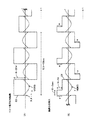
次に、本発明の実施の形態について説明する。図1は本発明になる液晶表示装置の一実施の形態の構成図を示す。同図において、LCOS(Liquid Crystal On Silicon)1は位相補償板2を介して偏光ビームスプリッタ(PBS)3の反射光路上に設けられている。PBS3の透過光路上には投射レンズ4が設けられている。
Next, an embodiment of the present invention will be described. FIG. 1 shows a configuration diagram of an embodiment of a liquid crystal display device according to the present invention. In the figure, an LCOS (Liquid Crystal On Silicon) 1 is provided on a reflection optical path of a polarization beam splitter (PBS) 3 via a
また、青色光を発光する複数の発光ダイオード(LED)が2次元アレイ状に配列された青色光用LEDアレイ光源5Bと、緑色光を発光する複数の発光ダイオード(LED)が2次元アレイ状に配列された緑色光用LEDアレイ光源5Gと、赤色光を発光する複数の発光ダイオード(LED)が2次元アレイ状に配列された赤色光用LEDアレイ光源5Rとは、フィールド毎に切替駆動され、LEDアレイ光源5Bからの青色光Bと、LEDアレイ光源5Gからの緑色光Gと、LEDアレイ光源5Rからの赤色光Rが、それぞれ偏光板6B、6G、6Rを通してダイクロイッククロスプリズム7に順次切り替えられて入射する構成とされている。
Also, a blue light LED
上記のダイクロイッククロスプリズム7は、青色光B及び赤色光Rをそれぞれ反射し、緑色光Gは透過してそれぞれ照明レンズ8を通してPBS3に入射する。PBS3は順次切替入射した各原色光を反射して位相補償板2を通してLCOS1に入射する。上記のダイクロイッククロスプリズム7は、照明レンズ8と共に照明系を構成している。
The dichroic cross prism 7 reflects blue light B and red light R, transmits green light G, and enters the
ここで、ランプではアーク長が短く点光源に近いが、LEDアレイ光源5B、5G、5Rは面光源となる。本実施の形態では、この面光源での光を有効に利用するため、照明レンズ8の前後の焦点面にLEDアレイ光源5B、5G、5RとLCOS1とが配置される。
Here, the lamp has a short arc length and is close to a point light source, but the LED
面光源の使用は、LCOS1に入射する光の入射角を大きくする。ホメオトロピック配向されたLCOS1中の液晶に斜め方向から光が入ると、電圧無印加時でも実効的に光学位相差が生じ、それにより変調を受けて出射する光がコントラストを低下させるので、位相補償板2を用いた光学補償により、この種の光漏れを防いでいる。
Use of a surface light source increases the incident angle of light incident on the
ここで、LCOSは、一般的にはシリコンのCMOS基板(第1の基板)上にマトリクス状にMOS型トランジスタや画素電極を設け、このCMOS基板と対向配置した第2の基板の画素電極対向面に光学的に透明の共通電極を設け、上記の2枚の基板間に封入された液晶層からなる反射型液晶表示素子であるが、本実施の形態のLCOS1も基本的な構造は一般的なLCOSと同様であるが、第1の基板上に設けられる単位画素の等価回路が図2で示されるように、2個のMOS型トランジスタTR1及びTR2で構成され、画面全体を一度に書き換える一括転送方式のLCOSである。
Here, the LCOS is generally a MOS-type transistor or pixel electrode provided in a matrix on a silicon CMOS substrate (first substrate), and a pixel electrode facing surface of a second substrate disposed opposite to the CMOS substrate. This is a reflective liquid crystal display element comprising a liquid crystal layer sealed between the two substrates, provided with an optically transparent common electrode, but the basic structure of the
図2の単位画素の等価回路について更に説明するに、第1のMOS型トランジスタTR1は、ゲートが水平方向に配置された走査信号線SCANに接続され、ソースが垂直方向に配置された画像信号線VIDEOに接続され、ドレインが電荷蓄積用コンデンサCの一端に接続されている。また、第2のMOS型トランジスタTR2は、ゲートが水平方向に配置された同期信号線SYNCに接続され、ソースが電荷蓄積用コンデンサCの一端に接続され、ドレインが液晶セルLCの一端(画素電極)に接続されている。液晶セルLCの他端(共通電極)には電圧CEが印加される。 The equivalent circuit of the unit pixel of FIG. 2 will be described further. The first MOS transistor TR1 has an image signal line in which the gate is connected to the scanning signal line SCAN arranged in the horizontal direction and the source is arranged in the vertical direction. The drain is connected to one end of the charge storage capacitor C. The drain is connected to VIDEO. The second MOS transistor TR2 has a gate connected to a synchronization signal line SYNC arranged in the horizontal direction, a source connected to one end of the charge storage capacitor C, and a drain connected to one end (pixel electrode) of the liquid crystal cell LC. )It is connected to the. The voltage CE is applied to the other end (common electrode) of the liquid crystal cell LC.
液晶セルLCは、第2の基板上の上記の透明の共通電極と、共通電極に対向する第1の基板上に設けられた画素電極と、それらの基板間に封入された液晶層からなる。この液晶層は、前述したスプレイ配向の状態又はベンド配向の状態となっている。 The liquid crystal cell LC includes the transparent common electrode on the second substrate, the pixel electrode provided on the first substrate facing the common electrode, and a liquid crystal layer sealed between the substrates. This liquid crystal layer is in the above-described splay alignment state or bend alignment state.
一括転送方式の駆動方法について説明するに、走査信号線SCANに接続されるトランジスタTR1の走査信号を印加すると共に、画像信号線VIDEOに単色画像に対応する画像信号を供給し、選択された走査信号線SCAN上にある横1列の画素のコンデンサCにトランジスタTR1のソース及びドレインを通して画像信号を書き込む。 The collective transfer type driving method will be described. A scanning signal of the transistor TR1 connected to the scanning signal line SCAN is applied, and an image signal corresponding to a single color image is supplied to the image signal line VIDEO, and the selected scanning signal is selected. An image signal is written through the source and drain of the transistor TR1 to the capacitor C of the pixel in the horizontal row on the line SCAN.
この動作を走査信号線SCAN毎に進め、すべての走査信号線SCAN上にある各列の画素のコンデンサCへの書き込みが終了した時点で、すべての画素に一斉に同期信号線SYNCから同期信号をトランジスタTR2のゲートに印加する。これにより、すべての画素のコンデンサCに蓄積されていた単色画像に対応する電荷が、すべての画素のトランジスタTR2のソース及びドレインを通して一度に画素電極に印加されて液晶セルLCに書き込まれ、画面全体への単色画像の書き込みが同時に完了する。 This operation is advanced for each scanning signal line SCAN, and when the writing to the capacitors C of the pixels in each column on all the scanning signal lines SCAN is completed, a synchronizing signal is simultaneously sent from the synchronizing signal line SYNC to all the pixels. Applied to the gate of transistor TR2. As a result, the charges corresponding to the monochromatic image stored in the capacitors C of all the pixels are applied to the pixel electrodes at once through the sources and drains of the transistors TR2 of all the pixels, and are written in the liquid crystal cell LC. Writing of a monochrome image to the camera is completed at the same time.
この一括転送方式では共通電極の電圧CEを可変できるので、本実施の形態では図3(A)に示すように、映像信号線VIDEOには点線Iで示すような通常の映像信号を供給しておき、液晶層をスプレイ配向からベンド配向に転移させるスタート時に、映像信号に対して6V〜20V程度の電位差を与える電圧CEを0.5秒〜60秒間共通電極に印加することにより、ペンド配向に相転移させる。 Since in this batch transfer method capable of varying the voltage CE of the common electrode, in this embodiment, as shown in FIG. 3 (A), the video signal line VIDEO supplies normal video signal as shown by dotted lines I In addition, at the start of transition of the liquid crystal layer from the splay alignment to the bend alignment, a voltage CE that gives a potential difference of about 6 V to 20 V with respect to the video signal is applied to the common electrode for 0.5 seconds to 60 seconds, thereby changing the pen alignment. Phase transition.
従って、本実施の形態によれば、従来のような映像信号ラインとは別にベンド配向に転移させるための電圧供給ラインを用意することなく、既存の共通電極の電圧CEを変化させることにより、短時間でベンド配向に転移させることができる。 Therefore, according to the present embodiment, the voltage CE of the existing common electrode can be changed without preparing a voltage supply line for shifting to bend orientation separately from the conventional video signal line. The bend orientation can be changed over time.
また、本実施の形態では、図3(B)に示すように、映像信号線VIDEOに供給される点線IIで示す映像信号の極性反転の直後に、共通電極に印加する電圧CEに、0〜3Vの波高値(絶対値)で幅2秒程度以下のパルスaを重畳する。これにより、黒表示の挿入ができ、液晶セルLCをより高速応答させると共に、黒表示の挿入による動画性能の向上ができる。 In this embodiment, as shown in FIG. 3B, the voltage CE applied to the common electrode is set to 0 to 0 immediately after the polarity inversion of the video signal indicated by the dotted line II supplied to the video signal line VIDEO. A pulse a having a peak value (absolute value) of 3 V and a width of about 2 seconds or less is superimposed. As a result, black display can be inserted, the liquid crystal cell LC can be made to respond at higher speed, and the moving image performance can be improved by inserting the black display.
次に、本発明の他の実施の形態について説明する。前述したように、従来のフィールドシーケンシャル表示方式では、1フレーム期間を3原色に対応した3フィールドに分割して液晶セルに各原色画像データを切り替えて供給すると共に、それと同期させて各原色光を液晶セルに照射するようにしているが、この実施の形態では、前述した図3(A)、(B)に示した駆動方法による液晶セルの高速応答性を利用し、1フレーム期間を4フィールドに分割し、例えば図4(A)に示すように、1フィールド毎に画像表示色を、赤、緑、青、緑の順で切り替えたり、あるいは、図4(B)に示すように、1フィールド毎に画像表示色を、赤、緑、赤、青の順で切り替える。 Next, another embodiment of the present invention will be described. As described above, in the conventional field sequential display system, one frame period is divided into three fields corresponding to the three primary colors, and each primary color image data is switched and supplied to the liquid crystal cell, and each primary color light is synchronized with that. Although the liquid crystal cell is irradiated, in this embodiment, one frame period is divided into four fields by utilizing the high-speed response of the liquid crystal cell by the driving method shown in FIGS. 3 (A) and 3 (B). For example, as shown in FIG. 4A, the image display color is switched in order of red, green, blue, and green as shown in FIG. 4A. Alternatively, as shown in FIG. The image display color is switched in order of red, green, red, and blue for each field.
すなわち、通常は1フィールド内で極性反転しながらR(+)R(−)→G(+)G(−)→B(+)B(−)と各フィールド毎に切り替えて1フレーム期間に各原色画像を1回ずつ表示するところを、1フレーム期間を4分割した各フィールド毎に、図4(A)では、R(+)R(−)→G(+)G(−)→B(+)B(−)→G(+)G(−)と表示する。この場合は、視感度の高い緑色画像を1フレーム期間に2回表示するので、従来に比べて表示を明るく感じさせることができ、照明光の利用効率を向上できる。 That is, normally, the polarity is reversed within one field while switching from R (+) R (−) → G (+) G (−) → B (+) B (−) for each field. In FIG. 4 (A), the primary color image is displayed once for each field obtained by dividing one frame period into four in FIG. 4 (A): R (+) R (−) → G (+) G (−) → B ( +) B (−) → G (+) G (−) is displayed. In this case, since a green image with high visibility is displayed twice in one frame period, it is possible to make the display feel brighter than in the past and to improve the use efficiency of illumination light.
同様に、図4(B)は、R(+)R(−)→G(+)G(−)→R(+)R(−)→B(+)B(−)と表示する場合を示しており、この場合は赤色画像を1フレーム期間に2回表示するので、3原色光のうち赤色光の光強度が最も弱い場合に、色バランスをとることができ、照明光の利用効率を向上できる。 Similarly, FIG. 4B illustrates a case where R (+) R (−) → G (+) G (−) → R (+) R (−) → B (+) B (−) is displayed. In this case, since the red image is displayed twice in one frame period, when the light intensity of the red light is the weakest among the three primary color lights, the color balance can be taken and the use efficiency of the illumination light can be improved. It can be improved.
また、上記以外にも、輝度や演色性の向上、あるいはフィールドシーケンシャル方式特有のいわゆるカラーブレイクを低減するためなどを目的として種々の表示方法があり、例えば、1フレーム期間を6フィールドに分割し、各フィールド毎にR(+)R(−)→G(+)G(−)→B(+)B(−)→R(+)R(−)→G(+)G(−)→B(+)B(−)と表示することも可能である。 In addition to the above, there are various display methods for the purpose of improving luminance and color rendering properties, or reducing so-called color breaks peculiar to the field sequential method. For example, one frame period is divided into 6 fields, R (+) R (−) → G (+) G (−) → B (+) B (−) → R (+) R (−) → G (+) G (−) → B for each field (+) B (-) can also be displayed.
再び図1に戻って説明するに、各フィールド期間毎に上記のように赤色、緑色、青色の3原色の画像データでLCOS1の液晶パネルを切り替えていくと共に、これに同期させてLCOS1の液晶パネル面に照射する各原色光を順次に切り替えることにより、LCOS1から反射されたフィールド毎に切り替わる各原色光の反射光は、位相補償板2を通してPBS3に入射して透過され、更に投射レンズ4を通して図示しないスクリーンに投射されカラー画像を表示する。
Returning to FIG. 1 again, the LCOS1 liquid crystal panel is switched by the image data of the three primary colors red, green and blue as described above for each field period, and the LCOS1 liquid crystal panel is synchronized with this. By sequentially switching each primary color light irradiated on the surface, the reflected light of each primary color switched for each field reflected from the
この実施の形態では、LEDを光源に用いているので、光源にランプを使用した場合に比しスイッチングが速いので、赤色・緑色・青色の順次点滅ができ、また色純度が高いので画像の色再現範囲を広くでき、またランプを使用した場合に必要となる色分解系が不要で、液晶表示装置の小型軽量化が可能となり、また消費電力も低減できる。更に、光源は面光源を用いているので1個のLEDを用いた場合よりも充分な光量が得られる。 In this embodiment, since an LED is used as a light source, switching is faster than when a lamp is used as the light source, so that red, green, and blue can be sequentially blinked, and the color purity of the image is high. The reproduction range can be widened, the color separation system required when using a lamp is unnecessary, the liquid crystal display device can be reduced in size and weight, and the power consumption can be reduced. Furthermore, since the surface light source is used as the light source, a sufficient amount of light can be obtained as compared with the case where one LED is used.
なお、本発明は上記の実施の形態に限定されるものではなく、例えば1フレーム期間を4フィールド以上に分割して各フィールド毎に原色画像を切替表示するフィールドシーケンシャル表示方式であればよく、また、黒表示の挿入は1フレーム期間を3フィールドに分割して各フィールド毎に原色画像を切替表示する従来のフィールドシーケンシャル表示方式の液晶表示装置にも適用できる。 Note that the present invention is not limited to the above embodiment, and may be any field sequential display method in which one frame period is divided into four fields or more and primary color images are switched and displayed for each field. The black display insertion can also be applied to a conventional field sequential display type liquid crystal display device in which one frame period is divided into three fields and the primary color image is switched and displayed for each field.
1 LCOS(Liquid Crystal On Silicon)
2 位相補償板
3 偏光ビームスプリッタ(PBS)
4 投射レンズ
5B、5G、5R LEDアレイ光源
6B、6G、6R 偏光板
7 ダイクロイッククロスプリズム
8 照明レンズ
TR1、TR2 MOS型トランジスタ
C 電荷蓄積用コンデンサ
LC 液晶セル
CE 共通電極への印加電圧
a 黒表示用パルス
1 LCOS (Liquid Crystal On Silicon)
2
4
Claims (2)
電荷蓄積用コンデンサと、走査信号入力時に前記電荷蓄積用コンデンサに映像信号データを書き込む第1のトランジスタと、同期信号入力時に前記電荷蓄積用コンデンサに書き込まれた映像信号データを前記液晶表示素子に供給する第2のトランジスタとからなる、前記第1の基板上に形成された画素回路と、
全画素の前記電荷蓄積用コンデンサに映像信号データを書き込んでから全画素の前記第2のトランジスタに前記同期信号を同時に入力することにより、前記電荷蓄積用コンデンサに書き込まれた映像信号データを、前記第1の基板上に設けられた全画素の前記画素電極に一斉に転送すると共に、前記液晶層のスプレイ配向からヘンド配向への転移スタート時から第1の所定期間は、前記第2の基板上に設けられた前記共通電極への印加電圧を前記第1の所定期間経過後よりも大なる値として前記液晶表示素子を駆動する駆動手段と、
前記フィールドシーケンシャル表示に基づき、前記液晶表示素子に照射される原色光の切り替えに同期して切替入力される、前記照射される原色光に対応した一の原色の映像信号データの極性反転の直後より1/2フィールド期間よりも短い第2の所定期間、一定の波高値のパルスを、前記第2の基板上に設けられた前記共通電極への印加電圧に重畳するパルス重畳手段と
を有することを特徴とする液晶表示装置。 A reflective liquid crystal display having a structure in which a liquid crystal layer is sealed between a first substrate on which at least a transistor and a pixel electrode are formed and a second substrate on which a common electrode is formed on the opposite surface of the first substrate. In a liquid crystal display device that includes an element and displays a color image by a field sequential method,
A charge storage capacitor; a first transistor for writing video signal data to the charge storage capacitor when a scanning signal is input; and a video signal data written to the charge storage capacitor when a synchronization signal is input to the liquid crystal display element A pixel circuit formed on the first substrate, the second circuit comprising:
By writing the video signal data to the charge storage capacitors of all pixels and then simultaneously inputting the synchronization signal to the second transistors of all pixels, the video signal data written to the charge storage capacitors is In addition to the simultaneous transfer to the pixel electrodes of all the pixels provided on the first substrate, the first predetermined period from the start of the transition from the splay alignment to the bend alignment of the liquid crystal layer is on the second substrate. Driving means for driving the liquid crystal display element with a voltage applied to the common electrode provided to the common electrode larger than that after the first predetermined period has elapsed;
Based on the field sequential display, immediately after the polarity inversion of the video signal data of one primary color corresponding to the irradiated primary color light, which is input in synchronization with the switching of the primary color light irradiated to the liquid crystal display element. Pulse superimposing means for superimposing a pulse having a constant peak value on a voltage applied to the common electrode provided on the second substrate for a second predetermined period shorter than a ½ field period. A characteristic liquid crystal display device.
前記照明手段により前記液晶表示素子に照射される原色光の切り替えに同期して、前記照射される原色光に対応した一の原色の映像信号データを各フィールド毎に順次切り替えて、前記第1の基板上に設けられた全画素の前記電荷蓄積用コンデンサに蓄積するデータ供給手段と In synchronization with switching of the primary color light irradiated to the liquid crystal display element by the illumination means, the video signal data of one primary color corresponding to the irradiated primary color light is sequentially switched for each field, and the first Data supply means for storing in the charge storage capacitors of all pixels provided on the substrate;
を更に有することを特徴とする請求項1記載の液晶表示装置。 The liquid crystal display device according to claim 1, further comprising:
Priority Applications (1)
| Application Number | Priority Date | Filing Date | Title |
|---|---|---|---|
| JP2003420352A JP4453356B2 (en) | 2003-12-18 | 2003-12-18 | Liquid crystal display |
Applications Claiming Priority (1)
| Application Number | Priority Date | Filing Date | Title |
|---|---|---|---|
| JP2003420352A JP4453356B2 (en) | 2003-12-18 | 2003-12-18 | Liquid crystal display |
Publications (2)
| Publication Number | Publication Date |
|---|---|
| JP2005181559A JP2005181559A (en) | 2005-07-07 |
| JP4453356B2 true JP4453356B2 (en) | 2010-04-21 |
Family
ID=34781911
Family Applications (1)
| Application Number | Title | Priority Date | Filing Date |
|---|---|---|---|
| JP2003420352A Expired - Fee Related JP4453356B2 (en) | 2003-12-18 | 2003-12-18 | Liquid crystal display |
Country Status (1)
| Country | Link |
|---|---|
| JP (1) | JP4453356B2 (en) |
Families Citing this family (6)
| Publication number | Priority date | Publication date | Assignee | Title |
|---|---|---|---|---|
| JP2006162639A (en) * | 2004-12-02 | 2006-06-22 | Hitachi Displays Ltd | Liquid crystal display device and projector |
| KR101152130B1 (en) * | 2005-08-05 | 2012-06-15 | 삼성전자주식회사 | Thin film transistor array panel for display device and manufacturing method thereof |
| KR100658276B1 (en) | 2005-11-23 | 2006-12-14 | 삼성에스디아이 주식회사 | Liquid crystal display and driving method thereof |
| KR100730175B1 (en) * | 2005-12-07 | 2007-06-19 | 삼성에스디아이 주식회사 | Method for transient driving of optically compensated birefringence liquid crystal display and apparatus thereof |
| KR100751352B1 (en) | 2005-12-07 | 2007-08-22 | 삼성에스디아이 주식회사 | Method for transient driving of optically compensated birefringence liquid crystal display and apparatus thereof |
| KR101227602B1 (en) | 2006-02-02 | 2013-01-29 | 삼성전자주식회사 | Field sequential color image display and method for driving the same |
-
2003
- 2003-12-18 JP JP2003420352A patent/JP4453356B2/en not_active Expired - Fee Related
Also Published As
| Publication number | Publication date |
|---|---|
| JP2005181559A (en) | 2005-07-07 |
Similar Documents
| Publication | Publication Date | Title |
|---|---|---|
| US7746294B2 (en) | Transflective liquid crystal display | |
| JP3956337B2 (en) | Frame sequential color display | |
| JP3308880B2 (en) | Liquid crystal display and projection type liquid crystal display | |
| KR100331486B1 (en) | Liquuid Crystal Display Apparatus and Liquid Crystal Display Projector the same including | |
| JP4297100B2 (en) | Electro-optical device, driving method thereof, and electronic apparatus | |
| RU2487379C1 (en) | Stereoscopic display device | |
| JP2004233555A (en) | Display device and display method | |
| JP4239892B2 (en) | Electro-optical device, driving method thereof, projection display device, and electronic apparatus | |
| JP2004191836A (en) | Display device and display method | |
| CN101379426A (en) | Liquid crystal display device | |
| US20090128472A1 (en) | Liquid crystal display device and related operating method | |
| US9607563B2 (en) | Liquid crystal display device, method for driving liquid crystal display device, and electronic apparatus | |
| JP2010091967A (en) | Electro-optical device | |
| JP2009075392A (en) | Electro-optical device and method for driving the same, and electronic apparatus | |
| JP2004004216A (en) | Liquid crystal display device | |
| TW200529136A (en) | Display device, method of driving the same, and projection display device | |
| JP3891000B2 (en) | Liquid crystal display device and driving method thereof | |
| JP4453356B2 (en) | Liquid crystal display | |
| JP4122911B2 (en) | Liquid crystal display device and liquid crystal panel | |
| JP2012058335A (en) | Electro-optical device and electronic apparatus | |
| JP2005055828A (en) | Image display device, its driving method, and projection display apparatus | |
| JP2006195387A (en) | Electro-optical device and electronic equipment | |
| JP2008261944A (en) | Liquid crystal display | |
| JP2004021025A (en) | Image display device and driving method for the same | |
| JP2001092427A (en) | Driving method of liquid crystal display device |
Legal Events
| Date | Code | Title | Description |
|---|---|---|---|
| A621 | Written request for application examination |
Free format text: JAPANESE INTERMEDIATE CODE: A621 Effective date: 20060331 |
|
| A977 | Report on retrieval |
Free format text: JAPANESE INTERMEDIATE CODE: A971007 Effective date: 20090821 |
|
| A131 | Notification of reasons for refusal |
Free format text: JAPANESE INTERMEDIATE CODE: A131 Effective date: 20090929 |
|
| A521 | Request for written amendment filed |
Free format text: JAPANESE INTERMEDIATE CODE: A523 Effective date: 20091119 |
|
| TRDD | Decision of grant or rejection written | ||
| A01 | Written decision to grant a patent or to grant a registration (utility model) |
Free format text: JAPANESE INTERMEDIATE CODE: A01 Effective date: 20100112 |
|
| A01 | Written decision to grant a patent or to grant a registration (utility model) |
Free format text: JAPANESE INTERMEDIATE CODE: A01 |
|
| A61 | First payment of annual fees (during grant procedure) |
Free format text: JAPANESE INTERMEDIATE CODE: A61 Effective date: 20100125 |
|
| FPAY | Renewal fee payment (event date is renewal date of database) |
Free format text: PAYMENT UNTIL: 20130212 Year of fee payment: 3 |
|
| R151 | Written notification of patent or utility model registration |
Ref document number: 4453356 Country of ref document: JP Free format text: JAPANESE INTERMEDIATE CODE: R151 |
|
| FPAY | Renewal fee payment (event date is renewal date of database) |
Free format text: PAYMENT UNTIL: 20130212 Year of fee payment: 3 |
|
| FPAY | Renewal fee payment (event date is renewal date of database) |
Free format text: PAYMENT UNTIL: 20130212 Year of fee payment: 3 |
|
| S111 | Request for change of ownership or part of ownership |
Free format text: JAPANESE INTERMEDIATE CODE: R313111 |
|
| FPAY | Renewal fee payment (event date is renewal date of database) |
Free format text: PAYMENT UNTIL: 20130212 Year of fee payment: 3 |
|
| R350 | Written notification of registration of transfer |
Free format text: JAPANESE INTERMEDIATE CODE: R350 |
|
| FPAY | Renewal fee payment (event date is renewal date of database) |
Free format text: PAYMENT UNTIL: 20130212 Year of fee payment: 3 |
|
| FPAY | Renewal fee payment (event date is renewal date of database) |
Free format text: PAYMENT UNTIL: 20140212 Year of fee payment: 4 |
|
| LAPS | Cancellation because of no payment of annual fees |