US7741164B2 - Method for fabricating SOI device - Google Patents
Method for fabricating SOI device Download PDFInfo
- Publication number
- US7741164B2 US7741164B2 US12/033,060 US3306008A US7741164B2 US 7741164 B2 US7741164 B2 US 7741164B2 US 3306008 A US3306008 A US 3306008A US 7741164 B2 US7741164 B2 US 7741164B2
- Authority
- US
- United States
- Prior art keywords
- monocrystalline silicon
- gate electrode
- layer
- spacer
- silicon layer
- Prior art date
- Legal status (The legal status is an assumption and is not a legal conclusion. Google has not performed a legal analysis and makes no representation as to the accuracy of the status listed.)
- Active, expires
Links
- 238000000034 method Methods 0.000 title claims abstract description 52
- 229910021421 monocrystalline silicon Inorganic materials 0.000 claims abstract description 78
- 239000000758 substrate Substances 0.000 claims abstract description 64
- 125000006850 spacer group Chemical group 0.000 claims abstract description 28
- 239000012212 insulator Substances 0.000 claims abstract description 21
- 239000004065 semiconductor Substances 0.000 claims abstract description 20
- 239000007772 electrode material Substances 0.000 claims abstract description 12
- 238000001459 lithography Methods 0.000 claims abstract description 6
- 150000002500 ions Chemical class 0.000 claims description 40
- 238000002955 isolation Methods 0.000 claims description 22
- 239000012535 impurity Substances 0.000 claims description 18
- 229910052751 metal Inorganic materials 0.000 claims description 18
- 239000002184 metal Substances 0.000 claims description 18
- 238000005530 etching Methods 0.000 claims description 15
- 239000002019 doping agent Substances 0.000 claims description 14
- 229910021332 silicide Inorganic materials 0.000 claims description 13
- FVBUAEGBCNSCDD-UHFFFAOYSA-N silicide(4-) Chemical compound [Si-4] FVBUAEGBCNSCDD-UHFFFAOYSA-N 0.000 claims description 13
- 238000000059 patterning Methods 0.000 claims description 9
- 238000005468 ion implantation Methods 0.000 claims description 8
- 239000011810 insulating material Substances 0.000 claims description 7
- 238000000151 deposition Methods 0.000 claims description 6
- 239000007943 implant Substances 0.000 claims 8
- 229920002120 photoresistant polymer Polymers 0.000 description 18
- XUIMIQQOPSSXEZ-UHFFFAOYSA-N Silicon Chemical compound [Si] XUIMIQQOPSSXEZ-UHFFFAOYSA-N 0.000 description 11
- 229910052710 silicon Inorganic materials 0.000 description 11
- 239000010703 silicon Substances 0.000 description 11
- VYPSYNLAJGMNEJ-UHFFFAOYSA-N Silicium dioxide Chemical compound O=[Si]=O VYPSYNLAJGMNEJ-UHFFFAOYSA-N 0.000 description 10
- 239000000463 material Substances 0.000 description 8
- 229910021420 polycrystalline silicon Inorganic materials 0.000 description 7
- 230000015572 biosynthetic process Effects 0.000 description 5
- -1 oxygen ions Chemical class 0.000 description 4
- 239000000377 silicon dioxide Substances 0.000 description 4
- 235000012239 silicon dioxide Nutrition 0.000 description 4
- 238000010438 heat treatment Methods 0.000 description 3
- 238000004518 low pressure chemical vapour deposition Methods 0.000 description 3
- 238000004519 manufacturing process Methods 0.000 description 3
- 230000000873 masking effect Effects 0.000 description 3
- UFHFLCQGNIYNRP-UHFFFAOYSA-N Hydrogen Chemical compound [H][H] UFHFLCQGNIYNRP-UHFFFAOYSA-N 0.000 description 2
- PXHVJJICTQNCMI-UHFFFAOYSA-N Nickel Chemical compound [Ni] PXHVJJICTQNCMI-UHFFFAOYSA-N 0.000 description 2
- KDLHZDBZIXYQEI-UHFFFAOYSA-N Palladium Chemical compound [Pd] KDLHZDBZIXYQEI-UHFFFAOYSA-N 0.000 description 2
- RTAQQCXQSZGOHL-UHFFFAOYSA-N Titanium Chemical compound [Ti] RTAQQCXQSZGOHL-UHFFFAOYSA-N 0.000 description 2
- 238000005229 chemical vapour deposition Methods 0.000 description 2
- 239000004020 conductor Substances 0.000 description 2
- 238000007796 conventional method Methods 0.000 description 2
- 230000005669 field effect Effects 0.000 description 2
- 229910052739 hydrogen Inorganic materials 0.000 description 2
- 239000001257 hydrogen Substances 0.000 description 2
- 229910052760 oxygen Inorganic materials 0.000 description 2
- 239000001301 oxygen Substances 0.000 description 2
- 238000000206 photolithography Methods 0.000 description 2
- 238000000623 plasma-assisted chemical vapour deposition Methods 0.000 description 2
- 229910052814 silicon oxide Inorganic materials 0.000 description 2
- 229910052719 titanium Inorganic materials 0.000 description 2
- 239000010936 titanium Substances 0.000 description 2
- OKTJSMMVPCPJKN-UHFFFAOYSA-N Carbon Chemical compound [C] OKTJSMMVPCPJKN-UHFFFAOYSA-N 0.000 description 1
- XPDWGBQVDMORPB-UHFFFAOYSA-N Fluoroform Chemical compound FC(F)F XPDWGBQVDMORPB-UHFFFAOYSA-N 0.000 description 1
- 229910004129 HfSiO Inorganic materials 0.000 description 1
- GRYLNZFGIOXLOG-UHFFFAOYSA-N Nitric acid Chemical compound O[N+]([O-])=O GRYLNZFGIOXLOG-UHFFFAOYSA-N 0.000 description 1
- 229910052581 Si3N4 Inorganic materials 0.000 description 1
- QAOWNCQODCNURD-UHFFFAOYSA-N Sulfuric acid Chemical compound OS(O)(=O)=O QAOWNCQODCNURD-UHFFFAOYSA-N 0.000 description 1
- BOTDANWDWHJENH-UHFFFAOYSA-N Tetraethyl orthosilicate Chemical compound CCO[Si](OCC)(OCC)OCC BOTDANWDWHJENH-UHFFFAOYSA-N 0.000 description 1
- NRTOMJZYCJJWKI-UHFFFAOYSA-N Titanium nitride Chemical compound [Ti]#N NRTOMJZYCJJWKI-UHFFFAOYSA-N 0.000 description 1
- 229910052785 arsenic Inorganic materials 0.000 description 1
- QVGXLLKOCUKJST-UHFFFAOYSA-N atomic oxygen Chemical compound [O] QVGXLLKOCUKJST-UHFFFAOYSA-N 0.000 description 1
- 229910052796 boron Inorganic materials 0.000 description 1
- 229910052799 carbon Inorganic materials 0.000 description 1
- 229910017052 cobalt Inorganic materials 0.000 description 1
- 239000010941 cobalt Substances 0.000 description 1
- GUTLYIVDDKVIGB-UHFFFAOYSA-N cobalt atom Chemical compound [Co] GUTLYIVDDKVIGB-UHFFFAOYSA-N 0.000 description 1
- 230000000295 complement effect Effects 0.000 description 1
- 239000003989 dielectric material Substances 0.000 description 1
- 229910052732 germanium Inorganic materials 0.000 description 1
- GNPVGFCGXDBREM-UHFFFAOYSA-N germanium atom Chemical compound [Ge] GNPVGFCGXDBREM-UHFFFAOYSA-N 0.000 description 1
- 238000002513 implantation Methods 0.000 description 1
- 229910044991 metal oxide Inorganic materials 0.000 description 1
- 150000004706 metal oxides Chemical class 0.000 description 1
- 229910052759 nickel Inorganic materials 0.000 description 1
- 229910017604 nitric acid Inorganic materials 0.000 description 1
- 230000001590 oxidative effect Effects 0.000 description 1
- 229910052763 palladium Inorganic materials 0.000 description 1
- 229910052698 phosphorus Inorganic materials 0.000 description 1
- 239000011574 phosphorus Substances 0.000 description 1
- 238000001020 plasma etching Methods 0.000 description 1
- 238000004151 rapid thermal annealing Methods 0.000 description 1
- HQVNEWCFYHHQES-UHFFFAOYSA-N silicon nitride Chemical compound N12[Si]34N5[Si]62N3[Si]51N64 HQVNEWCFYHHQES-UHFFFAOYSA-N 0.000 description 1
- 239000002210 silicon-based material Substances 0.000 description 1
- 239000000126 substance Substances 0.000 description 1
- WFKWXMTUELFFGS-UHFFFAOYSA-N tungsten Chemical compound [W] WFKWXMTUELFFGS-UHFFFAOYSA-N 0.000 description 1
- 229910052721 tungsten Inorganic materials 0.000 description 1
- 239000010937 tungsten Substances 0.000 description 1
- 238000001039 wet etching Methods 0.000 description 1
Images


Classifications
-
- H—ELECTRICITY
- H01—ELECTRIC ELEMENTS
- H01L—SEMICONDUCTOR DEVICES NOT COVERED BY CLASS H10
- H01L21/00—Processes or apparatus adapted for the manufacture or treatment of semiconductor or solid state devices or of parts thereof
- H01L21/70—Manufacture or treatment of devices consisting of a plurality of solid state components formed in or on a common substrate or of parts thereof; Manufacture of integrated circuit devices or of parts thereof
- H01L21/77—Manufacture or treatment of devices consisting of a plurality of solid state components or integrated circuits formed in, or on, a common substrate
- H01L21/78—Manufacture or treatment of devices consisting of a plurality of solid state components or integrated circuits formed in, or on, a common substrate with subsequent division of the substrate into plural individual devices
- H01L21/82—Manufacture or treatment of devices consisting of a plurality of solid state components or integrated circuits formed in, or on, a common substrate with subsequent division of the substrate into plural individual devices to produce devices, e.g. integrated circuits, each consisting of a plurality of components
- H01L21/822—Manufacture or treatment of devices consisting of a plurality of solid state components or integrated circuits formed in, or on, a common substrate with subsequent division of the substrate into plural individual devices to produce devices, e.g. integrated circuits, each consisting of a plurality of components the substrate being a semiconductor, using silicon technology
- H01L21/8232—Field-effect technology
- H01L21/8234—MIS technology, i.e. integration processes of field effect transistors of the conductor-insulator-semiconductor type
- H01L21/823481—MIS technology, i.e. integration processes of field effect transistors of the conductor-insulator-semiconductor type isolation region manufacturing related aspects, e.g. to avoid interaction of isolation region with adjacent structure
-
- H—ELECTRICITY
- H01—ELECTRIC ELEMENTS
- H01L—SEMICONDUCTOR DEVICES NOT COVERED BY CLASS H10
- H01L21/00—Processes or apparatus adapted for the manufacture or treatment of semiconductor or solid state devices or of parts thereof
- H01L21/02—Manufacture or treatment of semiconductor devices or of parts thereof
- H01L21/027—Making masks on semiconductor bodies for further photolithographic processing not provided for in group H01L21/18 or H01L21/34
- H01L21/033—Making masks on semiconductor bodies for further photolithographic processing not provided for in group H01L21/18 or H01L21/34 comprising inorganic layers
-
- H—ELECTRICITY
- H01—ELECTRIC ELEMENTS
- H01L—SEMICONDUCTOR DEVICES NOT COVERED BY CLASS H10
- H01L21/00—Processes or apparatus adapted for the manufacture or treatment of semiconductor or solid state devices or of parts thereof
- H01L21/02—Manufacture or treatment of semiconductor devices or of parts thereof
- H01L21/04—Manufacture or treatment of semiconductor devices or of parts thereof the devices having potential barriers, e.g. a PN junction, depletion layer or carrier concentration layer
- H01L21/18—Manufacture or treatment of semiconductor devices or of parts thereof the devices having potential barriers, e.g. a PN junction, depletion layer or carrier concentration layer the devices having semiconductor bodies comprising elements of Group IV of the Periodic Table or AIIIBV compounds with or without impurities, e.g. doping materials
- H01L21/20—Deposition of semiconductor materials on a substrate, e.g. epitaxial growth solid phase epitaxy
-
- H—ELECTRICITY
- H01—ELECTRIC ELEMENTS
- H01L—SEMICONDUCTOR DEVICES NOT COVERED BY CLASS H10
- H01L21/00—Processes or apparatus adapted for the manufacture or treatment of semiconductor or solid state devices or of parts thereof
- H01L21/70—Manufacture or treatment of devices consisting of a plurality of solid state components formed in or on a common substrate or of parts thereof; Manufacture of integrated circuit devices or of parts thereof
- H01L21/77—Manufacture or treatment of devices consisting of a plurality of solid state components or integrated circuits formed in, or on, a common substrate
- H01L21/78—Manufacture or treatment of devices consisting of a plurality of solid state components or integrated circuits formed in, or on, a common substrate with subsequent division of the substrate into plural individual devices
- H01L21/82—Manufacture or treatment of devices consisting of a plurality of solid state components or integrated circuits formed in, or on, a common substrate with subsequent division of the substrate into plural individual devices to produce devices, e.g. integrated circuits, each consisting of a plurality of components
- H01L21/84—Manufacture or treatment of devices consisting of a plurality of solid state components or integrated circuits formed in, or on, a common substrate with subsequent division of the substrate into plural individual devices to produce devices, e.g. integrated circuits, each consisting of a plurality of components the substrate being other than a semiconductor body, e.g. being an insulating body
-
- H—ELECTRICITY
- H01—ELECTRIC ELEMENTS
- H01L—SEMICONDUCTOR DEVICES NOT COVERED BY CLASS H10
- H01L27/00—Devices consisting of a plurality of semiconductor or other solid-state components formed in or on a common substrate
- H01L27/02—Devices consisting of a plurality of semiconductor or other solid-state components formed in or on a common substrate including semiconductor components specially adapted for rectifying, oscillating, amplifying or switching and having potential barriers; including integrated passive circuit elements having potential barriers
- H01L27/12—Devices consisting of a plurality of semiconductor or other solid-state components formed in or on a common substrate including semiconductor components specially adapted for rectifying, oscillating, amplifying or switching and having potential barriers; including integrated passive circuit elements having potential barriers the substrate being other than a semiconductor body, e.g. an insulating body
- H01L27/1203—Devices consisting of a plurality of semiconductor or other solid-state components formed in or on a common substrate including semiconductor components specially adapted for rectifying, oscillating, amplifying or switching and having potential barriers; including integrated passive circuit elements having potential barriers the substrate being other than a semiconductor body, e.g. an insulating body the substrate comprising an insulating body on a semiconductor body, e.g. SOI
- H01L27/1207—Devices consisting of a plurality of semiconductor or other solid-state components formed in or on a common substrate including semiconductor components specially adapted for rectifying, oscillating, amplifying or switching and having potential barriers; including integrated passive circuit elements having potential barriers the substrate being other than a semiconductor body, e.g. an insulating body the substrate comprising an insulating body on a semiconductor body, e.g. SOI combined with devices in contact with the semiconductor body, i.e. bulk/SOI hybrid circuits
-
- H—ELECTRICITY
- H01—ELECTRIC ELEMENTS
- H01L—SEMICONDUCTOR DEVICES NOT COVERED BY CLASS H10
- H01L29/00—Semiconductor devices specially adapted for rectifying, amplifying, oscillating or switching and having potential barriers; Capacitors or resistors having potential barriers, e.g. a PN-junction depletion layer or carrier concentration layer; Details of semiconductor bodies or of electrodes thereof ; Multistep manufacturing processes therefor
- H01L29/66—Types of semiconductor device ; Multistep manufacturing processes therefor
- H01L29/66007—Multistep manufacturing processes
- H01L29/66075—Multistep manufacturing processes of devices having semiconductor bodies comprising group 14 or group 13/15 materials
- H01L29/66083—Multistep manufacturing processes of devices having semiconductor bodies comprising group 14 or group 13/15 materials the devices being controllable only by variation of the electric current supplied or the electric potential applied, to one or more of the electrodes carrying the current to be rectified, amplified, oscillated or switched, e.g. two-terminal devices
- H01L29/6609—Diodes
- H01L29/66128—Planar diodes
-
- H—ELECTRICITY
- H01—ELECTRIC ELEMENTS
- H01L—SEMICONDUCTOR DEVICES NOT COVERED BY CLASS H10
- H01L29/00—Semiconductor devices specially adapted for rectifying, amplifying, oscillating or switching and having potential barriers; Capacitors or resistors having potential barriers, e.g. a PN-junction depletion layer or carrier concentration layer; Details of semiconductor bodies or of electrodes thereof ; Multistep manufacturing processes therefor
- H01L29/66—Types of semiconductor device ; Multistep manufacturing processes therefor
- H01L29/86—Types of semiconductor device ; Multistep manufacturing processes therefor controllable only by variation of the electric current supplied, or only the electric potential applied, to one or more of the electrodes carrying the current to be rectified, amplified, oscillated or switched
- H01L29/861—Diodes
- H01L29/8611—Planar PN junction diodes
-
- H—ELECTRICITY
- H01—ELECTRIC ELEMENTS
- H01L—SEMICONDUCTOR DEVICES NOT COVERED BY CLASS H10
- H01L21/00—Processes or apparatus adapted for the manufacture or treatment of semiconductor or solid state devices or of parts thereof
- H01L21/02—Manufacture or treatment of semiconductor devices or of parts thereof
- H01L21/04—Manufacture or treatment of semiconductor devices or of parts thereof the devices having potential barriers, e.g. a PN junction, depletion layer or carrier concentration layer
- H01L21/18—Manufacture or treatment of semiconductor devices or of parts thereof the devices having potential barriers, e.g. a PN junction, depletion layer or carrier concentration layer the devices having semiconductor bodies comprising elements of Group IV of the Periodic Table or AIIIBV compounds with or without impurities, e.g. doping materials
- H01L21/28—Manufacture of electrodes on semiconductor bodies using processes or apparatus not provided for in groups H01L21/20 - H01L21/268
- H01L21/28008—Making conductor-insulator-semiconductor electrodes
- H01L21/28017—Making conductor-insulator-semiconductor electrodes the insulator being formed after the semiconductor body, the semiconductor being silicon
- H01L21/28026—Making conductor-insulator-semiconductor electrodes the insulator being formed after the semiconductor body, the semiconductor being silicon characterised by the conductor
- H01L21/28123—Lithography-related aspects, e.g. sub-lithography lengths; Isolation-related aspects, e.g. to solve problems arising at the crossing with the side of the device isolation; Planarisation aspects
-
- H—ELECTRICITY
- H01—ELECTRIC ELEMENTS
- H01L—SEMICONDUCTOR DEVICES NOT COVERED BY CLASS H10
- H01L27/00—Devices consisting of a plurality of semiconductor or other solid-state components formed in or on a common substrate
- H01L27/02—Devices consisting of a plurality of semiconductor or other solid-state components formed in or on a common substrate including semiconductor components specially adapted for rectifying, oscillating, amplifying or switching and having potential barriers; including integrated passive circuit elements having potential barriers
- H01L27/04—Devices consisting of a plurality of semiconductor or other solid-state components formed in or on a common substrate including semiconductor components specially adapted for rectifying, oscillating, amplifying or switching and having potential barriers; including integrated passive circuit elements having potential barriers the substrate being a semiconductor body
- H01L27/06—Devices consisting of a plurality of semiconductor or other solid-state components formed in or on a common substrate including semiconductor components specially adapted for rectifying, oscillating, amplifying or switching and having potential barriers; including integrated passive circuit elements having potential barriers the substrate being a semiconductor body including a plurality of individual components in a non-repetitive configuration
- H01L27/0611—Devices consisting of a plurality of semiconductor or other solid-state components formed in or on a common substrate including semiconductor components specially adapted for rectifying, oscillating, amplifying or switching and having potential barriers; including integrated passive circuit elements having potential barriers the substrate being a semiconductor body including a plurality of individual components in a non-repetitive configuration integrated circuits having a two-dimensional layout of components without a common active region
- H01L27/0617—Devices consisting of a plurality of semiconductor or other solid-state components formed in or on a common substrate including semiconductor components specially adapted for rectifying, oscillating, amplifying or switching and having potential barriers; including integrated passive circuit elements having potential barriers the substrate being a semiconductor body including a plurality of individual components in a non-repetitive configuration integrated circuits having a two-dimensional layout of components without a common active region comprising components of the field-effect type
- H01L27/0629—Devices consisting of a plurality of semiconductor or other solid-state components formed in or on a common substrate including semiconductor components specially adapted for rectifying, oscillating, amplifying or switching and having potential barriers; including integrated passive circuit elements having potential barriers the substrate being a semiconductor body including a plurality of individual components in a non-repetitive configuration integrated circuits having a two-dimensional layout of components without a common active region comprising components of the field-effect type in combination with diodes, or resistors, or capacitors
Definitions
- the present invention generally relates to a method for fabricating semiconductor on insulator (SOI) devices, and more particularly relates to a method for fabricating SOI integrated circuits having devices in both the thin SOI layer and the substrate.
- SOI semiconductor on insulator
- ICs integrated circuits
- FETs field effect transistors
- MOSFETs metal oxide semiconductor field effect transistors
- CMOS circuit complementary MOS or CMOS circuit.
- Certain improvements in performance of FET ICs can be realized by forming the FETs in a thin layer of semiconductor material overlying an insulator layer.
- SOI semiconductor on insulator
- Such semiconductor on insulator (SOI) FETs exhibit lower junction capacitance and hence can operate at higher speeds. It is advantageous in certain applications, however, to fabricate at least some devices in the semiconductor substrate that supports the insulator layer.
- the devices formed in the substrate may have better thermal properties and can support higher voltages than devices formed in the thin semiconductor layer.
- MOS transistors As the complexity of the integrated circuits increases, more and more MOS transistors are needed to implement the integrated circuit function. As more and more transistors are designed into the IC, it becomes important to shrink the size of individual MOS transistors so that the size of the IC remains reasonable and the IC can be reliably manufactured. Shrinking the size of an MOS transistor implies that the minimum feature size, that is, the minimum width of a line or the minimum spacing between lines, is reduced. MOS transistors have now been aggressively reduced to the point at which the gate electrode of the transistor is less than or equal to 45 nanometers (nm) in width. Methods previously used to fabricate devices in the substrate of an SOI structure, however, have not be able to achieve the same minimum feature size in substrate devices as are realized in the devices formed in the thin semiconductor layer.
- a method for fabricating a semiconductor on insulator (SOI) device includes, in one embodiment, providing a monocrystalline silicon substrate having a monocrystalline silicon layer overlying a monocrystalline silicon substrate and separated therefrom by a dielectric layer. A well region is ion implanted in the monocrystalline silicon substrate. A gate electrode material is deposited overlying the monocrystalline silicon layer. The gate electrode material is photolithographically patterned and etched using a minimum lithography feature size to form a first gate electrode, a second gate electrode and a spacer having the minimum lithography feature size. The gate electrode material is then isotropically etched to reduce the width of the first gate electrode, the second gate electrode and the spacer.
- SOI semiconductor on insulator
- FIG. 1-11 schematically illustrate, in cross section, process steps in accordance with various embodiments of the invention
- FIG. 12 illustrates, in cross section, a prior art substrate diode
- FIG. 13 schematically illustrates, in cross section, a substrate diode in accordance with an embodiment of the invention.
- FIGS. 1-11 schematically illustrate method steps for the manufacture of a CMOS integrated circuit 20 in accordance with various embodiments of the invention.
- MOS device properly refers to a device having a metal gate electrode and an oxide gate insulator, that term will be used throughout to refer to any semiconductor device that includes a conductive gate electrode (whether metal or other conductive material) that is positioned over a gate insulator (whether oxide or other insulator) which, in turn, is positioned over a semiconductor substrate.
- CMOS integrated circuit 20 only a small portion of CMOS integrated circuit 20 is illustrated.
- integrated circuit 20 is a CMOS circuit
- the invention is also applicable to the fabrication of a single channel type MOS circuit.
- the method in accordance with one embodiment of the invention begins with providing a semiconductor substrate 21 .
- the semiconductor substrate is preferably a silicon substrate with a monocrystalline silicon layer 22 formed overlying a monocrystalline silicon carrier substrate 24 .
- the terms “silicon layer” and “silicon substrate” will be used to encompass the relatively pure monocrystalline silicon materials typically used in the semiconductor industry as well as silicon admixed with other elements such as germanium, carbon, and the like to form substantially monocrystalline semiconductor material.
- Monocrystalline silicon layer 22 will be used in the formation of N-channel and P-channel MOS transistors.
- Monocrystalline silicon substrate 24 will be used for the formation of a substrate device herein illustrated as a PN junction diode.
- Monocrystalline silicon layer 22 can be formed, for example, by the well known layer transfer technique. In that technique hydrogen is implanted into a subsurface region of an oxidized monocrystalline silicon wafer. The implanted wafer is then flip bonded to monocrystalline silicon substrate 24 . A two phase heat treatment is then carried out to split the hydrogen implanted wafer along the implanted region and to strengthen the bonding, leaving a thin monocrystalline silicon layer 22 bonded to the monocrystalline silicon substrate and separated from the substrate by a dielectric insulating layer 26 . The monocrystalline silicon layer is then thinned and polished, for example by chemical mechanical planarization (CMP) techniques, to a thickness of about 50-300 nanometers (nm) depending on the circuit function being implemented.
- CMP chemical mechanical planarization
- Both the monocrystalline silicon layer and the monocrystalline silicon carrier substrate preferably have a resistivity of at least about 1-35 Ohms per square.
- the silicon can be impurity doped either N-type or P-type, but is preferably doped P-type.
- Dielectric insulating layer 26 typically silicon dioxide, preferably has a thickness of about 50-200 nm.
- monocrystalline semiconductor substrate 21 can be formed by the SIMOX process.
- the SIMOX process is a well known process in which oxygen ions are implanted into a sub-surface region of monocrystalline silicon substrate 24 .
- the monocrystalline silicon substrate and the implanted oxygen are subsequently heated to form a sub-surface silicon oxide dielectric layer 26 that electrically isolates SOI layer 22 from the remaining portion of monocrystalline silicon substrate 24 .
- the thickness of SOI layer 22 is determined by the energy of the implanted ions.
- Dielectric layer 26 is commonly referred to as a buried oxide or “BOX” and will so be referred to herein.
- dielectric isolation regions 28 , 30 extending through monocrystalline silicon layer 22 to dielectric layer or BOX 26 .
- the dielectric isolation regions are preferably formed by the well known shallow trench isolation (STI) technique in which trenches are etched into monocrystalline silicon layer 22 , the trenches are filled with a dielectric material such as deposited silicon dioxide, and the excess silicon dioxide is removed by CMP.
- STI regions 28 provide electrical isolation, as needed, between various devices of the CMOS circuit that are to be formed in monocrystalline silicon layer 22 .
- STI region 30 aids in electrically isolating the device to be formed in carrier substrate 24 from the devices to be formed in monocrystalline silicon layer 22 .
- portions of monocrystalline silicon layer 22 can be doped, for example by ion implantation, to form P-type regions 32 and N-type regions 34 .
- a layer 35 of photoresist is applied overlying the surface of monocrystalline silicon layer 22 and dielectric isolation regions 28 , 30 .
- the layer of photoresist is patterned to expose a portion of dielectric isolation region 30 as illustrated in FIG. 3 .
- the patterned photoresist is used as an ion implantation mask and conductivity determining ionic impurities are implanted, as indicated by arrows 36 , into the surface of monocrystalline silicon substrate 24 to form a doped region 37 .
- phosphorus ions can be implanted into the monocrystalline silicon substrate at an energy of about 200-300 KeV and dose of about 1 ⁇ 10 13 -2 ⁇ 10 14 cm ⁇ 2 to form an N-type doped region 37 .
- a layer of gate insulator material 38 is grown or deposited on the surface of silicon layer 22 .
- the gate insulator may be a thermally grown silicon dioxide formed by heating the silicon substrate in an oxidizing ambient, or may be a deposited insulator such as a silicon oxide, silicon oxynitride, silicon nitride, a high dielectric constant insulator such as HfSiO, or the like.
- Deposited insulators can be deposited by chemical vapor deposition (CVD), low pressure chemical vapor deposition (LPCVD), or plasma enhanced chemical vapor deposition (PECVD).
- the gate insulator material is typically 1-10 nanometers (nm) in thickness.
- gate insulator material 38 is a deposited layer that is deposited onto both the dielectric isolation regions 28 , 30 and the remaining monocrystalline silicon layer 22 . As is well known, a grown thermal oxide would be grown only on the monocrystalline silicon layer.
- a layer 39 of gate electrode forming material such as polycrystalline silicon is deposited overlying gate insulator material 38 , monocrystalline silicon layer 22 , and the dielectric isolation regions 28 , 30 . Layer 39 will hereinafter be referred to as a polycrystalline silicon layer although those of skill in the art will recognize that other conductive materials could be used as the gate electrode material.
- the layer of polycrystalline silicon is preferably deposited as undoped polycrystalline silicon and is subsequently impurity doped by ion implantation.
- Polycrystalline gate electrode layer 39 is patterned and etched to form a P-channel gate electrode 40 overlying N-type region 34 of monocrystalline silicon layer 22 , an N-channel gate electrode 42 overlying P-type region 32 of monocrystalline silicon layer 22 and a spacer 44 overlying dielectric isolation region 30 .
- the etching of polycrystalline gate electrodes is well advanced in the art so that gate lengths of only 45 nm or less can be achieved.
- Polycrystalline silicon gate electrode layer 39 is preferably etched using such well know and advanced patterning and etching techniques to preferably obtain gate electrodes 40 and 42 and spacer 44 , each having minimum feature size.
- Such advanced patterning and etching techniques generally involve patterning and etching the polycrystalline silicon using the minimum available photolithography exposure feature size followed by isotropically etching the polycrystalline silicon to further reduce the width of the resulting structure.
- a layer 46 of photoresist is applied to the structure and is patterned to expose a portion of dielectric isolation region 30 and spacer 44 .
- the patterned layer of photoresist and spacer 44 are used together as an etch mask to etch openings 48 and 50 through dielectric isolation region 30 and dielectric insulating layer 26 and to expose portions of impurity doped region 37 .
- Openings 48 and 50 are anisotropically etched through dielectric isolation region 30 and dielectric insulating layer 26 , preferably by reactive ion etching.
- the dielectric layers can be reactive ion etched, for example, using a CF 4 or CHF 3 chemistry.
- the spacing between openings 48 and 50 is determined, not by the spacing of openings in layer 46 of photoresist, but by the width of spacer 44 and hence, in accordance with an embodiment of the invention, is comparable to the minimum feature size.
- the spacing between openings 48 and 50 can thus be less than the minimum photolithographic feature spacing otherwise attainable through photolithographic patterning and etching alone.
- photoresist layer 52 After removing layer 46 of photoresist another layer 52 of photoresist can next be applied to the structure and patterned to expose one of openings 48 and 50 while masking the other of the openings.
- the photoresist layer is also patterned to expose one of regions 32 and 34 while masking the other of the regions.
- photoresist layer 52 has been patterned to expose opening 48 and P-type region 32 .
- Patterned photoresist layer 52 is used as an ion implantation mask and N-type impurity dopant ions, preferably arsenic ions, are implanted into the exposed areas as indicated by arrows 54 .
- the N-type impurity dopant ions form source 56 and drain 58 regions of an N-channel MOS transistor that are self aligned with gate electrode 42 and a cathode region 60 self aligned with one edge of spacer 44 .
- Layer 52 of photoresist is removed and another layer 62 of photoresist is applied to the structure and is patterned to expose the other of openings 48 and 50 and the other of regions 32 and 34 while masking the previously exposed opening and region.
- photoresist layer 62 is patterned to expose opening 50 and region 34 .
- Patterned photoresist layer 62 is used as an ion implantation mask and P-type impurity dopant ions, preferably boron ions, are implanted into the exposed areas as indicated by arrows 64 .
- the P-type impurity dopant ions form source 66 and drain 68 regions of a P-channel MOS transistor that are self aligned with gate electrode 40 and an anode region 70 self aligned with the other edge of spacer 44 .
- Photoresist layer 52 is removed and the ion implanted regions are heated, preferably by rapid thermal annealing, to activate the implanted ions.
- Other conventional method steps such as the formation of sidewall spacers on the gate electrodes, implantation of additional source and drain regions, removal of gate insulator material that is not disposed under a gate electrode, and the like, may now be carried out to complete the processing of the MOS transistors.
- a layer of silicide forming metal such as nickel, cobalt, titanium, palladium, or the like is deposited onto the structure and in contact with the ion implanted source, drain, anode and cathode regions as well as to gate electrodes 40 and 42 .
- the silicide forming metal preferably has a thickness of about 5-15 nm.
- the silicide forming metal is heated, preferably to a temperature of about 350°-500° C. to cause the metal to react with the silicon with which it is in contact to form a metal silicide contact region 72 at the surface of each of the ion implanted regions and on the gate electrodes as illustrated in FIG. 9 .
- the metal that is not in contact with silicon for example the metal that is deposited on the dielectric isolation regions, does not react during the heating step and is removed, for example by wet etching in a H 2 O 2 /H 2 SO 4 or HNO 3 /HCl solution.
- a layer 74 of insulating material is deposited and planarized to cover the contact regions.
- the insulating material can be deposited, for example, by low pressure chemical vapor deposition using a tetraethylorthosilicate source.
- Layer 74 is preferably planarized by CMP.
- a layer of photoresist (not illustrated) is applied to the surface of the planarized insulating material and is used as an etch mask to etch contact openings 76 that extend through the insulating material to the metal silicide contact regions.
- Contact plugs 78 are formed in each of contact openings 76 to allow electrical contact to the various device regions.
- the contact plugs can be formed, for example, by depositing successive layers of titanium, titanium nitride, and tungsten in known manner. The excess metal layers can then be removed by CMP to leave contact plugs 78 as illustrated in FIG. 11 .
- CMP CMP
- sidewall spacers may be formed at the edges of the gate electrodes and those spacers may be used as masks for additional ion implantations or to space the metal silicide contacts apart from the gate electrodes.
- Prior SOI integrated circuits have included diodes fabricated in the monocrystalline silicon substrate as well as other circuit components formed in the thin monocrystalline silicon layer overlying an insulating layer, but in fabricating such circuits the anode and cathode regions have been defined in the substrate by patterning and etching the overlying thin silicon layer and the insulating layer using conventional photolithography techniques. That is, the anode and cathode regions were defined by separate mask patterns that were, at best, spaced apart by a distance equal to the minimum feature size. By fabricating substrate devices using an embodiment of the invention, it is possible to reduce the spacing between regions in the substrate to a distance equal to the width of the minimum achievable gate length.
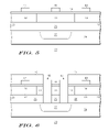
- FIG. 12 The benefit that can be realized by fabricating substrate devices in accordance with an embodiment of the invention can be seen by comparing a substrate diode fabricated by the conventional method, as illustrated in FIG. 12 with the substrate diode fabricated in accordance with an embodiment of the invention as illustrated in FIG. 13 .
- FIGS. 12 and 13 only the diode portion of the SOI integrated circuit is illustrated.
- FIG. 13 the same numbering has been used as was used in FIG. 11 ; corresponding regions in FIG. 12 have been given the same numbers.
Landscapes
- Engineering & Computer Science (AREA)
- Power Engineering (AREA)
- Microelectronics & Electronic Packaging (AREA)
- Condensed Matter Physics & Semiconductors (AREA)
- General Physics & Mathematics (AREA)
- Physics & Mathematics (AREA)
- Computer Hardware Design (AREA)
- Manufacturing & Machinery (AREA)
- Ceramic Engineering (AREA)
- Chemical & Material Sciences (AREA)
- Inorganic Chemistry (AREA)
- Thin Film Transistor (AREA)
- Metal-Oxide And Bipolar Metal-Oxide Semiconductor Integrated Circuits (AREA)
- Element Separation (AREA)
Abstract
A method is provided for fabricating a semiconductor on insulator (SOI) device. The method includes, in one embodiment, providing a monocrystalline silicon substrate having a monocrystalline silicon layer overlying a monocrystalline silicon substrate and separated therefrom by a dielectric layer. A well region is ion implanted in the monocrystalline silicon substrate. A gate electrode material is deposited overlying the monocrystalline silicon layer. The gate electrode material is photolithographically patterned and etched using a minimum lithography feature size to form a first gate electrode, a second gate electrode and a spacer having the minimum lithography feature size. The gate electrode material is then isotropically etched to reduce the width of the first gate electrode, the second gate electrode and the spacer.
Description
This is a continuation of U.S. patent application Ser. No. 11/127,329 filed May 11, 2005.
The present invention generally relates to a method for fabricating semiconductor on insulator (SOI) devices, and more particularly relates to a method for fabricating SOI integrated circuits having devices in both the thin SOI layer and the substrate.
The majority of present day integrated circuits (ICs) are implemented by using a plurality of interconnected field effect transistors (FETs), also called metal oxide semiconductor field effect transistors (MOSFETs or MOS transistors). The ICs are usually formed using both P-channel and N-channel FETs and the IC is then referred to as a complementary MOS or CMOS circuit. Certain improvements in performance of FET ICs can be realized by forming the FETs in a thin layer of semiconductor material overlying an insulator layer. Such semiconductor on insulator (SOI) FETs, for example, exhibit lower junction capacitance and hence can operate at higher speeds. It is advantageous in certain applications, however, to fabricate at least some devices in the semiconductor substrate that supports the insulator layer. The devices formed in the substrate, for example, may have better thermal properties and can support higher voltages than devices formed in the thin semiconductor layer.
As the complexity of the integrated circuits increases, more and more MOS transistors are needed to implement the integrated circuit function. As more and more transistors are designed into the IC, it becomes important to shrink the size of individual MOS transistors so that the size of the IC remains reasonable and the IC can be reliably manufactured. Shrinking the size of an MOS transistor implies that the minimum feature size, that is, the minimum width of a line or the minimum spacing between lines, is reduced. MOS transistors have now been aggressively reduced to the point at which the gate electrode of the transistor is less than or equal to 45 nanometers (nm) in width. Methods previously used to fabricate devices in the substrate of an SOI structure, however, have not be able to achieve the same minimum feature size in substrate devices as are realized in the devices formed in the thin semiconductor layer.
Accordingly, it is desirable to provide a method for fabricating SOI devices having minimum feature size. In addition, it is desirable to provide a self aligned method for fabricating SOI devices having minimum feature size substrate devices. Furthermore, other desirable features and characteristics of the present invention will become apparent from the subsequent detailed description and the appended claims, taken in conjunction with the accompanying drawings and the foregoing technical field and background.
A method is provided for fabricating a semiconductor on insulator (SOI) device. The method includes, in one embodiment, providing a monocrystalline silicon substrate having a monocrystalline silicon layer overlying a monocrystalline silicon substrate and separated therefrom by a dielectric layer. A well region is ion implanted in the monocrystalline silicon substrate. A gate electrode material is deposited overlying the monocrystalline silicon layer. The gate electrode material is photolithographically patterned and etched using a minimum lithography feature size to form a first gate electrode, a second gate electrode and a spacer having the minimum lithography feature size. The gate electrode material is then isotropically etched to reduce the width of the first gate electrode, the second gate electrode and the spacer.
The present invention will hereinafter be described in conjunction with the following drawing figures, wherein like numerals denote like elements, and wherein
The following detailed description is merely exemplary in nature and is not intended to limit the invention or the application and uses of the invention. Furthermore, there is no intention to be bound by any expressed or implied theory presented in the preceding technical field, background, brief summary or the following detailed description.
As illustrated in FIG. 1 , the method in accordance with one embodiment of the invention begins with providing a semiconductor substrate 21. The semiconductor substrate is preferably a silicon substrate with a monocrystalline silicon layer 22 formed overlying a monocrystalline silicon carrier substrate 24. As used herein, the terms “silicon layer” and “silicon substrate” will be used to encompass the relatively pure monocrystalline silicon materials typically used in the semiconductor industry as well as silicon admixed with other elements such as germanium, carbon, and the like to form substantially monocrystalline semiconductor material. Monocrystalline silicon layer 22 will be used in the formation of N-channel and P-channel MOS transistors. Monocrystalline silicon substrate 24 will be used for the formation of a substrate device herein illustrated as a PN junction diode. Monocrystalline silicon layer 22 can be formed, for example, by the well known layer transfer technique. In that technique hydrogen is implanted into a subsurface region of an oxidized monocrystalline silicon wafer. The implanted wafer is then flip bonded to monocrystalline silicon substrate 24. A two phase heat treatment is then carried out to split the hydrogen implanted wafer along the implanted region and to strengthen the bonding, leaving a thin monocrystalline silicon layer 22 bonded to the monocrystalline silicon substrate and separated from the substrate by a dielectric insulating layer 26. The monocrystalline silicon layer is then thinned and polished, for example by chemical mechanical planarization (CMP) techniques, to a thickness of about 50-300 nanometers (nm) depending on the circuit function being implemented. Both the monocrystalline silicon layer and the monocrystalline silicon carrier substrate preferably have a resistivity of at least about 1-35 Ohms per square. The silicon can be impurity doped either N-type or P-type, but is preferably doped P-type. Dielectric insulating layer 26, typically silicon dioxide, preferably has a thickness of about 50-200 nm.
As one alternative to the wafer bonding technique, monocrystalline semiconductor substrate 21 can be formed by the SIMOX process. The SIMOX process is a well known process in which oxygen ions are implanted into a sub-surface region of monocrystalline silicon substrate 24. The monocrystalline silicon substrate and the implanted oxygen are subsequently heated to form a sub-surface silicon oxide dielectric layer 26 that electrically isolates SOI layer 22 from the remaining portion of monocrystalline silicon substrate 24. The thickness of SOI layer 22 is determined by the energy of the implanted ions. Dielectric layer 26 is commonly referred to as a buried oxide or “BOX” and will so be referred to herein.
Having provided a semiconductor substrate 21, the method in accordance with one embodiment of the invention continues as illustrated in FIG. 2 by the formation of dielectric isolation regions 28, 30 extending through monocrystalline silicon layer 22 to dielectric layer or BOX 26. The dielectric isolation regions are preferably formed by the well known shallow trench isolation (STI) technique in which trenches are etched into monocrystalline silicon layer 22, the trenches are filled with a dielectric material such as deposited silicon dioxide, and the excess silicon dioxide is removed by CMP. STI regions 28 provide electrical isolation, as needed, between various devices of the CMOS circuit that are to be formed in monocrystalline silicon layer 22. In accordance with an embodiment of the invention, STI region 30 aids in electrically isolating the device to be formed in carrier substrate 24 from the devices to be formed in monocrystalline silicon layer 22. Either before or after the formation of dielectric isolation regions 28, 30, portions of monocrystalline silicon layer 22 can be doped, for example by ion implantation, to form P-type regions 32 and N-type regions 34.
In accordance with one embodiment of the invention, a layer 35 of photoresist is applied overlying the surface of monocrystalline silicon layer 22 and dielectric isolation regions 28, 30. The layer of photoresist is patterned to expose a portion of dielectric isolation region 30 as illustrated in FIG. 3 . The patterned photoresist is used as an ion implantation mask and conductivity determining ionic impurities are implanted, as indicated by arrows 36, into the surface of monocrystalline silicon substrate 24 to form a doped region 37. For example, phosphorus ions can be implanted into the monocrystalline silicon substrate at an energy of about 200-300 KeV and dose of about 1×10¹³-2×1014 cm−2 to form an N-type doped region 37.
As illustrated in FIG. 4 , after removing layer 35 of photoresist, a layer of gate insulator material 38 is grown or deposited on the surface of silicon layer 22. The gate insulator may be a thermally grown silicon dioxide formed by heating the silicon substrate in an oxidizing ambient, or may be a deposited insulator such as a silicon oxide, silicon oxynitride, silicon nitride, a high dielectric constant insulator such as HfSiO, or the like. Deposited insulators can be deposited by chemical vapor deposition (CVD), low pressure chemical vapor deposition (LPCVD), or plasma enhanced chemical vapor deposition (PECVD). The gate insulator material is typically 1-10 nanometers (nm) in thickness. As illustrated, gate insulator material 38 is a deposited layer that is deposited onto both the dielectric isolation regions 28, 30 and the remaining monocrystalline silicon layer 22. As is well known, a grown thermal oxide would be grown only on the monocrystalline silicon layer. A layer 39 of gate electrode forming material such as polycrystalline silicon is deposited overlying gate insulator material 38, monocrystalline silicon layer 22, and the dielectric isolation regions 28, 30. Layer 39 will hereinafter be referred to as a polycrystalline silicon layer although those of skill in the art will recognize that other conductive materials could be used as the gate electrode material. The layer of polycrystalline silicon is preferably deposited as undoped polycrystalline silicon and is subsequently impurity doped by ion implantation.
The method in accordance with an embodiment of the invention proceeds as illustrated in FIG. 5 . Polycrystalline gate electrode layer 39 is patterned and etched to form a P-channel gate electrode 40 overlying N-type region 34 of monocrystalline silicon layer 22, an N-channel gate electrode 42 overlying P-type region 32 of monocrystalline silicon layer 22 and a spacer 44 overlying dielectric isolation region 30. The etching of polycrystalline gate electrodes is well advanced in the art so that gate lengths of only 45 nm or less can be achieved. Polycrystalline silicon gate electrode layer 39 is preferably etched using such well know and advanced patterning and etching techniques to preferably obtain gate electrodes 40 and 42 and spacer 44, each having minimum feature size. Such advanced patterning and etching techniques generally involve patterning and etching the polycrystalline silicon using the minimum available photolithography exposure feature size followed by isotropically etching the polycrystalline silicon to further reduce the width of the resulting structure.
As illustrated in FIG. 6 , a layer 46 of photoresist is applied to the structure and is patterned to expose a portion of dielectric isolation region 30 and spacer 44. In accordance with an embodiment of the invention, the patterned layer of photoresist and spacer 44 are used together as an etch mask to etch openings 48 and 50 through dielectric isolation region 30 and dielectric insulating layer 26 and to expose portions of impurity doped region 37. Openings 48 and 50 are anisotropically etched through dielectric isolation region 30 and dielectric insulating layer 26, preferably by reactive ion etching. The dielectric layers can be reactive ion etched, for example, using a CF4 or CHF3 chemistry. The spacing between openings 48 and 50 is determined, not by the spacing of openings in layer 46 of photoresist, but by the width of spacer 44 and hence, in accordance with an embodiment of the invention, is comparable to the minimum feature size. The spacing between openings 48 and 50 can thus be less than the minimum photolithographic feature spacing otherwise attainable through photolithographic patterning and etching alone.
After removing layer 46 of photoresist another layer 52 of photoresist can next be applied to the structure and patterned to expose one of openings 48 and 50 while masking the other of the openings. The photoresist layer is also patterned to expose one of regions 32 and 34 while masking the other of the regions. As illustrated in FIG. 7 , photoresist layer 52 has been patterned to expose opening 48 and P-type region 32. Patterned photoresist layer 52 is used as an ion implantation mask and N-type impurity dopant ions, preferably arsenic ions, are implanted into the exposed areas as indicated by arrows 54. The N-type impurity dopant ions form source 56 and drain 58 regions of an N-channel MOS transistor that are self aligned with gate electrode 42 and a cathode region 60 self aligned with one edge of spacer 44.
In accordance with an embodiment of the invention a layer of silicide forming metal such as nickel, cobalt, titanium, palladium, or the like is deposited onto the structure and in contact with the ion implanted source, drain, anode and cathode regions as well as to gate electrodes 40 and 42. The silicide forming metal preferably has a thickness of about 5-15 nm. The silicide forming metal is heated, preferably to a temperature of about 350°-500° C. to cause the metal to react with the silicon with which it is in contact to form a metal silicide contact region 72 at the surface of each of the ion implanted regions and on the gate electrodes as illustrated in FIG. 9 . The metal that is not in contact with silicon, for example the metal that is deposited on the dielectric isolation regions, does not react during the heating step and is removed, for example by wet etching in a H2O2/H2SO4 or HNO3/HCl solution.
As illustrated in FIG. 10 a layer 74 of insulating material is deposited and planarized to cover the contact regions. The insulating material can be deposited, for example, by low pressure chemical vapor deposition using a tetraethylorthosilicate source. Layer 74 is preferably planarized by CMP. Following the planarization, a layer of photoresist (not illustrated) is applied to the surface of the planarized insulating material and is used as an etch mask to etch contact openings 76 that extend through the insulating material to the metal silicide contact regions.
Contact plugs 78 are formed in each of contact openings 76 to allow electrical contact to the various device regions. The contact plugs can be formed, for example, by depositing successive layers of titanium, titanium nitride, and tungsten in known manner. The excess metal layers can then be removed by CMP to leave contact plugs 78 as illustrated in FIG. 11 . Those of skill in the art will understand that contact openings 76 and contact plugs 78 may not be needed to contact each and every one of the silicide contact regions, but rather that such contacting will be dictated by the details of the circuit being implemented.
Those of skill in the art will appreciate that alternative and/or additional steps may be used to fabricate integrated circuit 20 and the order of the method steps may be changed without departing from the broad scope of the invention. For example, sidewall spacers may be formed at the edges of the gate electrodes and those spacers may be used as masks for additional ion implantations or to space the metal silicide contacts apart from the gate electrodes.
Prior SOI integrated circuits have included diodes fabricated in the monocrystalline silicon substrate as well as other circuit components formed in the thin monocrystalline silicon layer overlying an insulating layer, but in fabricating such circuits the anode and cathode regions have been defined in the substrate by patterning and etching the overlying thin silicon layer and the insulating layer using conventional photolithography techniques. That is, the anode and cathode regions were defined by separate mask patterns that were, at best, spaced apart by a distance equal to the minimum feature size. By fabricating substrate devices using an embodiment of the invention, it is possible to reduce the spacing between regions in the substrate to a distance equal to the width of the minimum achievable gate length. The benefit that can be realized by fabricating substrate devices in accordance with an embodiment of the invention can be seen by comparing a substrate diode fabricated by the conventional method, as illustrated in FIG. 12 with the substrate diode fabricated in accordance with an embodiment of the invention as illustrated in FIG. 13 . In FIGS. 12 and 13 only the diode portion of the SOI integrated circuit is illustrated. In FIG. 13 , the same numbering has been used as was used in FIG. 11 ; corresponding regions in FIG. 12 have been given the same numbers. The spacing between the anode and the cathode of the prior art device, indicated by double headed arrow 86, is two and one half to five times the spacing, indicated by the double headed arrow 88, between the anode and the cathode of the diode fabricated in accordance with an embodiment of the invention.
While at least one exemplary embodiment has been presented in the foregoing detailed description, it should be appreciated that a vast number of variations exist. It should also be appreciated that the exemplary embodiment or exemplary embodiments are only examples, and are not intended to limit the scope, applicability, or configuration of the invention in any way. Rather, the foregoing detailed description will provide those skilled in the art with a convenient road map for implementing the exemplary embodiment or exemplary embodiments. It should be understood that various changes can be made in the function and arrangement of elements without departing from the scope of the invention as set forth in the appended claims and the legal equivalents thereof.
Claims (20)
1. A method for fabricating a semiconductor on insulator (SOI) device having a monocrystalline silicon layer overlying a monocrystalline silicon substrate and separated therefrom by a dielectric layer, the method comprising the steps of:
ion implanting a well region in the monocrystalline silicon substrate;
then depositing a gate electrode material overlying the monocrystalline silicon layer;
photolithographically patterning and etching the gate electrode material using a minimum lithography feature size to form a first gate electrode, a second gate electrode and a spacer having the minimum lithography feature size; and
then isotropically etching the gate electrode material to reduce the width of the first gate electrode, the second gate electrode and the spacer.
2. The method of claim 1 further comprising the step of:
ion implanting impurity determining dopant ions into the monocrystalline silicon layer using the gate electrode as an ion implant mask to form spaced apart source and drain regions in the monocrystalline silicon layer.
3. The method of claim 2 further comprising the step of:
ion implanting impurity determining dopant ions into the monocrystalline silicon substrate using the spacer as an ion implant mask to form spaced apart device regions in the monocrystalline substrate.
4. The method of claim 3 further comprising the step of:
electrically contacting the spaced apart device regions.
5. The method of claim 2 wherein the step of ion implanting impurity determining dopant ions into the monocrystalline silicon layer using the gate electrode as an ion implant mask to form spaced apart source and drain regions in the monocrystalline silicon layer comprises the step of:
ion implanting N-type impurity determining dopant ions into the well region of the monocrystalline silicon substrate using the spacer as an ion implant mask to form an N-type device region in the well region of the monocrystalline silicon substrate and into the monocrystalline silicon layer using the first gate electrode as an ion implant mask to form N-channel source and drain regions in the monocrystalline silicon layer.
6. The method of claim 5 wherein the step of ion implanting impurity determining dopant ions into the monocrystalline silicon substrate using the spacer as an ion implant mask to form spaced apart device regions in the monocrystalline substrate comprises the step of:
ion implanting P-type impurity determining dopant ions into the well region of the monocrystalline silicon substrate using the spacer as an ion implant mask to form a P-type device region in the well region of the monocrystalline silicon substrate and into the monocrystalline silicon layer using the second gate electrode as an ion implant mask to form P-channel source and drain regions in the monocrystalline silicon layer.
7. A method for fabricating a semiconductor on insulator (SOI) device having a monocrystalline silicon layer overlying a monocrystalline silicon substrate and separated therefrom by a dielectric layer, the method comprising the steps of:
forming a dielectric isolation region extending through the monocrystalline silicon layer to the dielectric layer;
ion implanting a well region in the monocrystalline silicon substrate;
depositing a layer of gate electrode material overlying the monocrystalline silicon layer and the dielectric isolation region;
patterning the layer of gate electrode material to simultaneously form a gate electrode overlying the monocrystalline silicon layer and a spacer overlying the dielectric isolation region, wherein the gate electrode and the spacer each have a minimum width; and
etching the dielectric isolation region and the dielectric layer using the spacer as an etch mask.
8. The method of claim 7 further comprising the step of:
ion implanting impurity determining dopant ions using the spacer as an ion implantation mask to form spaced apart device regions in the monocrystalline silicon substrate and using the gate electrode as another ion implantation mask to form source and drain regions in the monocrystalline silicon layer proximate the gate electrode.
9. The method of claim 8 wherein the step of ion implanting impurity determining dopant ions to form spaced apart device regions comprises the steps of:
ion implanting a P-type region to form an anode of a substrate diode; and
ion implanting an N-type region to form a cathode of a substrate diode.
10. The method of claim 8 further comprising the step of:
forming a metal silicide layer on the spaced apart device regions.
11. The method of claim 10 further comprising the steps of:
depositing a layer of insulating material overlying the metal silicide layer;
planarizing the layer of insulating material;
etching openings through the layer of insulating material to expose the metal silicide layer; and
forming electrical contacts in the openings to electrically contact the device regions.
12. A method for fabricating a semiconductor on insulator (SOI) device having a monocrystalline silicon layer overlying a monocrystalline silicon substrate and separated therefrom by a dielectric layer, the method comprising the steps of:
forming a dielectric isolation region extending through the monocrystalline silicon layer to the dielectric layer;
ion implanting a well region in the monocrystalline silicon substrate;
depositing a gate electrode layer overlying the monocrystalline silicon layer and the dielectric isolation region;
patterning the gate electrode layer using a photolithographic patterning and etching process to form a P-channel gate electrode and an N-channel gate electrode overlying the monocrystalline silicon layer and a spacer overlying the dielectric isolation region, wherein the P-channel gate electrode, the N-channel gate electrode, and the spacer each have a minimum photolithographic feature size; and
subsequently isotropically etching the spacer to reduce the minimum photolithographic feature size.
13. The method of claim 12 further comprising the step of:
etching through the dielectric isolation region and the dielectric layer using the spacer as an etch mask to expose an anode region and a cathode region spaced apart in the well region of the monocrystalline silicon substrate.
14. The method of claim 13 further comprising the step of:
implanting P-type impurity dopants into the monocrystalline silicon layer to form source and drain regions of a P-channel MOS transistor proximate the P-channel gate electrode and into the anode region in the monocrystalline silicon substrate to form an anode of a substrate diode.
15. The method of claim 14 further comprising the step of:
implanting N-type impurity dopants into the monocrystalline silicon layer to form source and drain regions of an N-channel MOS transistor proximate the N-channel gate electrode and into the cathode region in the monocrystalline silicon substrate to form a cathode of a substrate diode.
16. The method of claim 15 further comprising the step of:
forming a metal silicide in electrical contact with the anode and the cathode.
17. The method of claim 16 further comprising the step of:
depositing an electrically insulating layer overlying the metal silicide.
18. The method of claim 17 further comprising the step of:
etching contact openings extending through the electrically insulating layer to expose a portion of the metal silicide.
19. The method of claim 18 further comprising the step of:
forming electrical contacts contacting the anode and the cathode through the contact openings.
20. The method of claim 19 wherein the step of forming electrical contacts comprises the step of forming conductive plugs filling the contact openings.
Priority Applications (1)
| Application Number | Priority Date | Filing Date | Title |
|---|---|---|---|
| US12/033,060 US7741164B2 (en) | 2005-05-11 | 2008-02-19 | Method for fabricating SOI device |
Applications Claiming Priority (2)
| Application Number | Priority Date | Filing Date | Title |
|---|---|---|---|
| US11/127,329 US7361534B2 (en) | 2005-05-11 | 2005-05-11 | Method for fabricating SOI device |
| US12/033,060 US7741164B2 (en) | 2005-05-11 | 2008-02-19 | Method for fabricating SOI device |
Related Parent Applications (1)
| Application Number | Title | Priority Date | Filing Date |
|---|---|---|---|
| US11/127,329 Continuation US7361534B2 (en) | 2005-05-11 | 2005-05-11 | Method for fabricating SOI device |
Publications (2)
| Publication Number | Publication Date |
|---|---|
| US20080138941A1 US20080138941A1 (en) | 2008-06-12 |
| US7741164B2 true US7741164B2 (en) | 2010-06-22 |
Family
ID=36716797
Family Applications (2)
| Application Number | Title | Priority Date | Filing Date |
|---|---|---|---|
| US11/127,329 Expired - Fee Related US7361534B2 (en) | 2005-05-11 | 2005-05-11 | Method for fabricating SOI device |
| US12/033,060 Active 2025-09-22 US7741164B2 (en) | 2005-05-11 | 2008-02-19 | Method for fabricating SOI device |
Family Applications Before (1)
| Application Number | Title | Priority Date | Filing Date |
|---|---|---|---|
| US11/127,329 Expired - Fee Related US7361534B2 (en) | 2005-05-11 | 2005-05-11 | Method for fabricating SOI device |
Country Status (8)
| Country | Link |
|---|---|
| US (2) | US7361534B2 (en) |
| JP (1) | JP5079687B2 (en) |
| KR (1) | KR101201489B1 (en) |
| CN (1) | CN100562988C (en) |
| DE (2) | DE112006001169B4 (en) |
| GB (1) | GB2440861B (en) |
| TW (1) | TWI390666B (en) |
| WO (1) | WO2006124182A1 (en) |
Cited By (4)
| Publication number | Priority date | Publication date | Assignee | Title |
|---|---|---|---|---|
| US20100156510A1 (en) * | 2008-12-23 | 2010-06-24 | International Business Machines Corporation | Soi radio frequency switch for reducing high frequency harmonics |
| US20100163994A1 (en) * | 2008-12-31 | 2010-07-01 | Andreas Kurz | Soi device with a buried insulating material having increased etch resistivity |
| US20120181655A1 (en) * | 2011-01-19 | 2012-07-19 | Globalfoundries Inc. | SOI Semiconductor Device Comprising a Substrate Diode and a Film Diode Formed by Using a Common Well Implantation Mask |
| US20130161746A1 (en) * | 2011-12-27 | 2013-06-27 | Commissariat A L'energie Atomique Et Aux Ene Alt | Transistor and method of fabrication |
Families Citing this family (26)
| Publication number | Priority date | Publication date | Assignee | Title |
|---|---|---|---|---|
| DE102007004859A1 (en) * | 2007-01-31 | 2008-08-14 | Advanced Micro Devices, Inc., Sunnyvale | Method for manufacturing silicon on insulator device used in thermal sensing applications involves forming metal silicide in transistors and doped regions |
| US7879663B2 (en) * | 2007-03-08 | 2011-02-01 | Freescale Semiconductor, Inc. | Trench formation in a semiconductor material |
| US20080247101A1 (en) * | 2007-04-09 | 2008-10-09 | Advanced Micro Devices, Inc. | Electronic device and method |
| DE102007052097B4 (en) * | 2007-10-31 | 2010-10-28 | Advanced Micro Devices, Inc., Sunnyvale | Method for producing an SOI device with a substrate diode |
| US7875913B2 (en) * | 2008-05-30 | 2011-01-25 | Omnivision Technologies, Inc. | Transistor with contact over gate active area |
| US8120110B2 (en) * | 2008-08-08 | 2012-02-21 | International Business Machines Corporation | Semiconductor structure including a high performance FET and a high voltage FET on a SOI substrate |
| US7999320B2 (en) * | 2008-12-23 | 2011-08-16 | International Business Machines Corporation | SOI radio frequency switch with enhanced signal fidelity and electrical isolation |
| US8299537B2 (en) * | 2009-02-11 | 2012-10-30 | International Business Machines Corporation | Semiconductor-on-insulator substrate and structure including multiple order radio frequency harmonic supressing region |
| ATE535937T1 (en) * | 2009-05-18 | 2011-12-15 | Soitec Silicon On Insulator | PRODUCTION PROCESS FOR A HYBRID SEMICONDUCTOR SUBSTRATE |
| US8048753B2 (en) * | 2009-06-12 | 2011-11-01 | Globalfoundries Inc. | Charging protection device |
| DE102009031114B4 (en) * | 2009-06-30 | 2011-07-07 | Globalfoundries Dresden Module One LLC & CO. KG, 01109 | A semiconductor element fabricated in a crystalline substrate material and having an embedded in situ n-doped semiconductor material, and methods of making the same |
| US7955940B2 (en) * | 2009-09-01 | 2011-06-07 | International Business Machines Corporation | Silicon-on-insulator substrate with built-in substrate junction |
| CN102792444B (en) * | 2010-03-09 | 2015-10-14 | 大学共同利用机关法人高能加速器研究机构 | The manufacture method of semiconductor device and semiconductor device |
| KR20160058499A (en) * | 2014-11-17 | 2016-05-25 | 삼성전자주식회사 | Semiconductor device, and method and apparatus for fabricating the same |
| US10446644B2 (en) * | 2015-06-22 | 2019-10-15 | Globalfoundries Inc. | Device structures for a silicon-on-insulator substrate with a high-resistance handle wafer |
| CN105185816A (en) * | 2015-10-15 | 2015-12-23 | 京东方科技集团股份有限公司 | Array substrate, manufacturing method, and display device |
| US11600234B2 (en) | 2015-10-15 | 2023-03-07 | Ordos Yuansheng Optoelectronics Co., Ltd. | Display substrate and driving method thereof |
| WO2021035420A1 (en) | 2019-08-23 | 2021-03-04 | 京东方科技集团股份有限公司 | Display panel and manufacturing method therefor, and display device |
| WO2021035414A1 (en) | 2019-08-23 | 2021-03-04 | 京东方科技集团股份有限公司 | Pixel circuit and driving method therefor, and display substrate and driving method therefor, and display device |
| US10418380B2 (en) | 2017-07-31 | 2019-09-17 | Globalfoundries Inc. | High-voltage transistor device with thick gate insulation layers |
| US10699963B2 (en) * | 2017-08-31 | 2020-06-30 | Taiwan Semiconductor Manufacturing Co., Ltd. | Structure and formation method of semiconductor device structure with isolation feature |
| US10115837B1 (en) * | 2017-09-28 | 2018-10-30 | Globalfoundries Singapore Pte. Ltd. | Integrated circuits with solar cells and methods for producing the same |
| JP7339432B2 (en) | 2019-08-23 | 2023-09-05 | 京東方科技集團股▲ふん▼有限公司 | Display device, manufacturing method thereof, drive substrate |
| CN112740421A (en) * | 2019-08-23 | 2021-04-30 | 京东方科技集团股份有限公司 | Display device and method for manufacturing the same |
| US11930664B2 (en) | 2019-08-23 | 2024-03-12 | Boe Technology Group Co., Ltd. | Display device with transistors oriented in directions intersecting direction of driving transistor and manufacturing method thereof |
| EP4024466A4 (en) | 2019-08-27 | 2022-10-05 | BOE Technology Group Co., Ltd. | Electronic device substrate and method for manufacture and electronic device thereof |
Citations (12)
| Publication number | Priority date | Publication date | Assignee | Title |
|---|---|---|---|---|
| EP0364393A2 (en) | 1988-10-12 | 1990-04-18 | Nippon Telegraph And Telephone Corporation | Power semiconductor device |
| US5847419A (en) | 1996-09-17 | 1998-12-08 | Kabushiki Kaisha Toshiba | Si-SiGe semiconductor device and method of fabricating the same |
| US5869379A (en) * | 1997-12-08 | 1999-02-09 | Advanced Micro Devices, Inc. | Method of forming air gap spacer for high performance MOSFETS' |
| US5869872A (en) * | 1995-07-10 | 1999-02-09 | Nippondenso Co., Ltd. | Semiconductor integrated circuit device and manufacturing method for the same |
| JPH11238860A (en) | 1998-02-19 | 1999-08-31 | Hitachi Ltd | Semiconductor integrated circuit device and its manufacture |
| US6124615A (en) | 1998-05-04 | 2000-09-26 | United Microelectronics Corp. | Stacked semiconductor structure for high integration of an integrated circuit with junction devices |
| US6303414B1 (en) * | 2000-07-12 | 2001-10-16 | Chartered Semiconductor Manufacturing Ltd. | Method of forming PID protection diode for SOI wafer |
| US6407429B1 (en) | 1999-10-20 | 2002-06-18 | Samsung Electronics Co., Ltd. | Semiconductor device having silicon on insulator and fabricating method therefor |
| US20020175378A1 (en) | 2001-05-22 | 2002-11-28 | Tae-Hee Choe | SOI substrate having an etch stop layer, and fabrication method thereof, SOI integrated circuit fabricated thereon, and method of fabricating SOI integrated circuit using the same |
| US20040043590A1 (en) | 2002-07-31 | 2004-03-04 | Advanced Micro Devices, Inc. | Method for semiconductor gate line dimension reduction |
| US6835662B1 (en) | 2003-07-14 | 2004-12-28 | Advanced Micro Devices, Inc. | Partially de-coupled core and periphery gate module process |
| US20050269642A1 (en) | 2004-06-03 | 2005-12-08 | Kabushiki Kaisha Toshiba | Semiconductor device |
Family Cites Families (6)
| Publication number | Priority date | Publication date | Assignee | Title |
|---|---|---|---|---|
| JPS6113662A (en) * | 1984-06-28 | 1986-01-21 | Nippon Telegr & Teleph Corp <Ntt> | Complementary type mis transistor device and manufacture thereof |
| JPH0738413B2 (en) * | 1984-10-31 | 1995-04-26 | 富士通株式会社 | Semiconductor device |
| JPH09115999A (en) * | 1995-10-23 | 1997-05-02 | Denso Corp | Semiconductor integrated circuit device |
| JP3415401B2 (en) * | 1997-08-28 | 2003-06-09 | 株式会社東芝 | Semiconductor integrated circuit device and method of manufacturing the same |
| JP2003224264A (en) * | 2002-01-29 | 2003-08-08 | Sony Corp | Semiconductor device and its manufacturing method |
| US6835622B2 (en) * | 2002-06-04 | 2004-12-28 | Taiwan Semiconductor Manufacturing Co., Ltd | Gate electrode doping method for forming semiconductor integrated circuit microelectronic fabrication with varying effective gate dielectric layer thicknesses |
-
2005
- 2005-05-11 US US11/127,329 patent/US7361534B2/en not_active Expired - Fee Related
-
2006
- 2006-04-19 JP JP2008511132A patent/JP5079687B2/en not_active Expired - Fee Related
- 2006-04-19 KR KR1020077028975A patent/KR101201489B1/en not_active IP Right Cessation
- 2006-04-19 DE DE112006001169T patent/DE112006001169B4/en not_active Expired - Fee Related
- 2006-04-19 DE DE112006004256T patent/DE112006004256A5/en active Pending
- 2006-04-19 WO PCT/US2006/014626 patent/WO2006124182A1/en active Application Filing
- 2006-04-19 CN CNB2006800163892A patent/CN100562988C/en not_active Expired - Fee Related
- 2006-04-19 GB GB0721841A patent/GB2440861B/en not_active Expired - Fee Related
- 2006-05-08 TW TW095116200A patent/TWI390666B/en not_active IP Right Cessation
-
2008
- 2008-02-19 US US12/033,060 patent/US7741164B2/en active Active
Patent Citations (15)
| Publication number | Priority date | Publication date | Assignee | Title |
|---|---|---|---|---|
| EP0364393A2 (en) | 1988-10-12 | 1990-04-18 | Nippon Telegraph And Telephone Corporation | Power semiconductor device |
| US5869872A (en) * | 1995-07-10 | 1999-02-09 | Nippondenso Co., Ltd. | Semiconductor integrated circuit device and manufacturing method for the same |
| US5847419A (en) | 1996-09-17 | 1998-12-08 | Kabushiki Kaisha Toshiba | Si-SiGe semiconductor device and method of fabricating the same |
| US5869379A (en) * | 1997-12-08 | 1999-02-09 | Advanced Micro Devices, Inc. | Method of forming air gap spacer for high performance MOSFETS' |
| JPH11238860A (en) | 1998-02-19 | 1999-08-31 | Hitachi Ltd | Semiconductor integrated circuit device and its manufacture |
| US6124615A (en) | 1998-05-04 | 2000-09-26 | United Microelectronics Corp. | Stacked semiconductor structure for high integration of an integrated circuit with junction devices |
| US20020119608A1 (en) * | 1999-10-20 | 2002-08-29 | Samsung Electronics Co., Ltd. | Semiconductor device having silicon on insulator and fabricating method therefor |
| US6407429B1 (en) | 1999-10-20 | 2002-06-18 | Samsung Electronics Co., Ltd. | Semiconductor device having silicon on insulator and fabricating method therefor |
| US20020022328A1 (en) | 2000-07-12 | 2002-02-21 | Chartered Semiconductor Manufacturing Ltd. | Method of forming PID protection diode for SOI wafer |
| US6303414B1 (en) * | 2000-07-12 | 2001-10-16 | Chartered Semiconductor Manufacturing Ltd. | Method of forming PID protection diode for SOI wafer |
| US6611024B2 (en) | 2000-07-12 | 2003-08-26 | Chartered Semiconductor Manufacturing Ltd. | Method of forming PID protection diode for SOI wafer |
| US20020175378A1 (en) | 2001-05-22 | 2002-11-28 | Tae-Hee Choe | SOI substrate having an etch stop layer, and fabrication method thereof, SOI integrated circuit fabricated thereon, and method of fabricating SOI integrated circuit using the same |
| US20040043590A1 (en) | 2002-07-31 | 2004-03-04 | Advanced Micro Devices, Inc. | Method for semiconductor gate line dimension reduction |
| US6835662B1 (en) | 2003-07-14 | 2004-12-28 | Advanced Micro Devices, Inc. | Partially de-coupled core and periphery gate module process |
| US20050269642A1 (en) | 2004-06-03 | 2005-12-08 | Kabushiki Kaisha Toshiba | Semiconductor device |
Cited By (10)
| Publication number | Priority date | Publication date | Assignee | Title |
|---|---|---|---|---|
| US20100156510A1 (en) * | 2008-12-23 | 2010-06-24 | International Business Machines Corporation | Soi radio frequency switch for reducing high frequency harmonics |
| US8026131B2 (en) * | 2008-12-23 | 2011-09-27 | International Business Machines Corporation | SOI radio frequency switch for reducing high frequency harmonics |
| US20100163994A1 (en) * | 2008-12-31 | 2010-07-01 | Andreas Kurz | Soi device with a buried insulating material having increased etch resistivity |
| US8617940B2 (en) * | 2008-12-31 | 2013-12-31 | Advanced Micro Devices, Inc. | SOI device with a buried insulating material having increased etch resistivity |
| US20120181655A1 (en) * | 2011-01-19 | 2012-07-19 | Globalfoundries Inc. | SOI Semiconductor Device Comprising a Substrate Diode and a Film Diode Formed by Using a Common Well Implantation Mask |
| US8536033B2 (en) * | 2011-01-19 | 2013-09-17 | Globalfoundries Inc. | SOI semiconductor device comprising a substrate diode and a film diode formed by using a common well implantation mask |
| US20130334604A1 (en) * | 2011-01-19 | 2013-12-19 | Global Foundries Inc. | Soi semiconductor device comprising a substrate diode and a film diode formed by using a common well implantation mask |
| US9082662B2 (en) * | 2011-01-19 | 2015-07-14 | Globalfoundries Inc. | SOI semiconductor device comprising a substrate diode and a film diode formed by using a common well implantation mask |
| US20130161746A1 (en) * | 2011-12-27 | 2013-06-27 | Commissariat A L'energie Atomique Et Aux Ene Alt | Transistor and method of fabrication |
| US9337350B2 (en) * | 2011-12-27 | 2016-05-10 | Commissariat A L'energie Atomique Et Aux Energies Alternatives | Transistor with reduced parasitic capacitance and access resistance of the source and drain, and method of fabrication of the same |
Also Published As
| Publication number | Publication date |
|---|---|
| CN100562988C (en) | 2009-11-25 |
| GB0721841D0 (en) | 2007-12-27 |
| JP5079687B2 (en) | 2012-11-21 |
| US20060258110A1 (en) | 2006-11-16 |
| DE112006001169T5 (en) | 2008-03-06 |
| US7361534B2 (en) | 2008-04-22 |
| GB2440861A (en) | 2008-02-13 |
| JP2008541446A (en) | 2008-11-20 |
| WO2006124182A1 (en) | 2006-11-23 |
| CN101180725A (en) | 2008-05-14 |
| TWI390666B (en) | 2013-03-21 |
| KR101201489B1 (en) | 2012-11-14 |
| DE112006004256A5 (en) | 2013-04-25 |
| TW200735263A (en) | 2007-09-16 |
| US20080138941A1 (en) | 2008-06-12 |
| GB2440861B (en) | 2010-06-16 |
| KR20080011227A (en) | 2008-01-31 |
| DE112006001169B4 (en) | 2012-04-26 |
Similar Documents
| Publication | Publication Date | Title |
|---|---|---|
| US7741164B2 (en) | Method for fabricating SOI device | |
| US7410859B1 (en) | Stressed MOS device and method for its fabrication | |
| US6972478B1 (en) | Integrated circuit and method for its manufacture | |
| US7326601B2 (en) | Methods for fabrication of a stressed MOS device | |
| US8395217B1 (en) | Isolation in CMOSFET devices utilizing buried air bags | |
| US7986008B2 (en) | SOI semiconductor components and methods for their fabrication | |
| US20090001420A1 (en) | Semiconductor device and method for manufacturing semiconductor device | |
| US7670914B2 (en) | Methods for fabricating multiple finger transistors | |
| US20140001561A1 (en) | Cmos devices having strain source/drain regions and low contact resistance | |
| US7919379B2 (en) | Dielectric spacer removal | |
| US7169676B1 (en) | Semiconductor devices and methods for forming the same including contacting gate to source | |
| US7977180B2 (en) | Methods for fabricating stressed MOS devices | |
| US20060272574A1 (en) | Methods for manufacturing integrated circuits | |
| US7465639B1 (en) | Method for fabricating an SOI device | |
| US7521380B2 (en) | Methods for fabricating a stress enhanced semiconductor device having narrow pitch and wide pitch transistors | |
| US11031406B2 (en) | Semiconductor devices having silicon/germanium active regions with different germanium concentrations | |
| US7465623B2 (en) | Methods for fabricating a semiconductor device on an SOI substrate | |
| US7432174B1 (en) | Methods for fabricating semiconductor substrates with silicon regions having differential crystallographic orientations | |
| US7670932B2 (en) | MOS structures with contact projections for lower contact resistance and methods for fabricating the same | |
| US8329519B2 (en) | Methods for fabricating a semiconductor device having decreased contact resistance | |
| US6169006B1 (en) | Semiconductor device having grown oxide spacers and method of manufacture thereof | |
| US6277698B1 (en) | Method of manufacturing semiconductor devices having uniform, fully doped gate electrodes | |
| US9653365B1 (en) | Methods for fabricating integrated circuits with low, medium, and/or high voltage transistors on an extremely thin silicon-on-insulator substrate | |
| US20080305613A1 (en) | Method for fabricating an soi defined semiconductor device |
Legal Events
| Date | Code | Title | Description |
|---|---|---|---|
| FEPP | Fee payment procedure |
Free format text: PAYOR NUMBER ASSIGNED (ORIGINAL EVENT CODE: ASPN); ENTITY STATUS OF PATENT OWNER: LARGE ENTITY |
|
| STCF | Information on status: patent grant |
Free format text: PATENTED CASE |
|
| FPAY | Fee payment |
Year of fee payment: 4 |
|
| MAFP | Maintenance fee payment |
Free format text: PAYMENT OF MAINTENANCE FEE, 8TH YEAR, LARGE ENTITY (ORIGINAL EVENT CODE: M1552) Year of fee payment: 8 |
|
| MAFP | Maintenance fee payment |
Free format text: PAYMENT OF MAINTENANCE FEE, 12TH YEAR, LARGE ENTITY (ORIGINAL EVENT CODE: M1553); ENTITY STATUS OF PATENT OWNER: LARGE ENTITY Year of fee payment: 12 |