US7719600B2 - Image capturing apparatus, control method therefor, and program regarding foreign substance removal - Google Patents
Image capturing apparatus, control method therefor, and program regarding foreign substance removal Download PDFInfo
- Publication number
- US7719600B2 US7719600B2 US11/739,394 US73939407A US7719600B2 US 7719600 B2 US7719600 B2 US 7719600B2 US 73939407 A US73939407 A US 73939407A US 7719600 B2 US7719600 B2 US 7719600B2
- Authority
- US
- United States
- Prior art keywords
- foreign substance
- image capturing
- instruction
- substance removing
- unit
- Prior art date
- Legal status (The legal status is an assumption and is not a legal conclusion. Google has not performed a legal analysis and makes no representation as to the accuracy of the status listed.)
- Expired - Fee Related, expires
Links
Images


Classifications
-
- G—PHYSICS
- G03—PHOTOGRAPHY; CINEMATOGRAPHY; ANALOGOUS TECHNIQUES USING WAVES OTHER THAN OPTICAL WAVES; ELECTROGRAPHY; HOLOGRAPHY
- G03B—APPARATUS OR ARRANGEMENTS FOR TAKING PHOTOGRAPHS OR FOR PROJECTING OR VIEWING THEM; APPARATUS OR ARRANGEMENTS EMPLOYING ANALOGOUS TECHNIQUES USING WAVES OTHER THAN OPTICAL WAVES; ACCESSORIES THEREFOR
- G03B17/00—Details of cameras or camera bodies; Accessories therefor
- G03B17/02—Bodies
-
- G—PHYSICS
- G02—OPTICS
- G02B—OPTICAL ELEMENTS, SYSTEMS OR APPARATUS
- G02B13/00—Optical objectives specially designed for the purposes specified below
- G02B13/16—Optical objectives specially designed for the purposes specified below for use in conjunction with image converters or intensifiers, or for use with projectors, e.g. objectives for projection TV
-
- G—PHYSICS
- G02—OPTICS
- G02B—OPTICAL ELEMENTS, SYSTEMS OR APPARATUS
- G02B27/00—Optical systems or apparatus not provided for by any of the groups G02B1/00 - G02B26/00, G02B30/00
- G02B27/0006—Optical systems or apparatus not provided for by any of the groups G02B1/00 - G02B26/00, G02B30/00 with means to keep optical surfaces clean, e.g. by preventing or removing dirt, stains, contamination, condensation
-
- G—PHYSICS
- G02—OPTICS
- G02B—OPTICAL ELEMENTS, SYSTEMS OR APPARATUS
- G02B7/00—Mountings, adjusting means, or light-tight connections, for optical elements
- G02B7/006—Filter holders
-
- G—PHYSICS
- G03—PHOTOGRAPHY; CINEMATOGRAPHY; ANALOGOUS TECHNIQUES USING WAVES OTHER THAN OPTICAL WAVES; ELECTROGRAPHY; HOLOGRAPHY
- G03B—APPARATUS OR ARRANGEMENTS FOR TAKING PHOTOGRAPHS OR FOR PROJECTING OR VIEWING THEM; APPARATUS OR ARRANGEMENTS EMPLOYING ANALOGOUS TECHNIQUES USING WAVES OTHER THAN OPTICAL WAVES; ACCESSORIES THEREFOR
- G03B17/00—Details of cameras or camera bodies; Accessories therefor
- G03B17/02—Bodies
- G03B17/12—Bodies with means for supporting objectives, supplementary lenses, filters, masks, or turrets
- G03B17/14—Bodies with means for supporting objectives, supplementary lenses, filters, masks, or turrets interchangeably
-
- G—PHYSICS
- G03—PHOTOGRAPHY; CINEMATOGRAPHY; ANALOGOUS TECHNIQUES USING WAVES OTHER THAN OPTICAL WAVES; ELECTROGRAPHY; HOLOGRAPHY
- G03B—APPARATUS OR ARRANGEMENTS FOR TAKING PHOTOGRAPHS OR FOR PROJECTING OR VIEWING THEM; APPARATUS OR ARRANGEMENTS EMPLOYING ANALOGOUS TECHNIQUES USING WAVES OTHER THAN OPTICAL WAVES; ACCESSORIES THEREFOR
- G03B17/00—Details of cameras or camera bodies; Accessories therefor
- G03B17/28—Locating light-sensitive material within camera
-
- G—PHYSICS
- G03—PHOTOGRAPHY; CINEMATOGRAPHY; ANALOGOUS TECHNIQUES USING WAVES OTHER THAN OPTICAL WAVES; ELECTROGRAPHY; HOLOGRAPHY
- G03B—APPARATUS OR ARRANGEMENTS FOR TAKING PHOTOGRAPHS OR FOR PROJECTING OR VIEWING THEM; APPARATUS OR ARRANGEMENTS EMPLOYING ANALOGOUS TECHNIQUES USING WAVES OTHER THAN OPTICAL WAVES; ACCESSORIES THEREFOR
- G03B19/00—Cameras
- G03B19/02—Still-picture cameras
- G03B19/12—Reflex cameras with single objective and a movable reflector or a partly-transmitting mirror
-
- H—ELECTRICITY
- H04—ELECTRIC COMMUNICATION TECHNIQUE
- H04N—PICTORIAL COMMUNICATION, e.g. TELEVISION
- H04N23/00—Cameras or camera modules comprising electronic image sensors; Control thereof
- H04N23/50—Constructional details
- H04N23/55—Optical parts specially adapted for electronic image sensors; Mounting thereof
-
- H—ELECTRICITY
- H04—ELECTRIC COMMUNICATION TECHNIQUE
- H04N—PICTORIAL COMMUNICATION, e.g. TELEVISION
- H04N23/00—Cameras or camera modules comprising electronic image sensors; Control thereof
- H04N23/60—Control of cameras or camera modules
- H04N23/65—Control of camera operation in relation to power supply
-
- H—ELECTRICITY
- H04—ELECTRIC COMMUNICATION TECHNIQUE
- H04N—PICTORIAL COMMUNICATION, e.g. TELEVISION
- H04N23/00—Cameras or camera modules comprising electronic image sensors; Control thereof
- H04N23/60—Control of cameras or camera modules
- H04N23/67—Focus control based on electronic image sensor signals
- H04N23/672—Focus control based on electronic image sensor signals based on the phase difference signals
-
- H—ELECTRICITY
- H04—ELECTRIC COMMUNICATION TECHNIQUE
- H04N—PICTORIAL COMMUNICATION, e.g. TELEVISION
- H04N23/00—Cameras or camera modules comprising electronic image sensors; Control thereof
- H04N23/80—Camera processing pipelines; Components thereof
- H04N23/81—Camera processing pipelines; Components thereof for suppressing or minimising disturbance in the image signal generation
- H04N23/811—Camera processing pipelines; Components thereof for suppressing or minimising disturbance in the image signal generation by dust removal, e.g. from surfaces of the image sensor or processing of the image signal output by the electronic image sensor
-
- H—ELECTRICITY
- H04—ELECTRIC COMMUNICATION TECHNIQUE
- H04N—PICTORIAL COMMUNICATION, e.g. TELEVISION
- H04N2101/00—Still video cameras
Definitions
- the present invention relates to a technique for removing a foreign substance such as dust adhering to the surface of an optical member inserted on the image capturing optical axis in an image capturing apparatus.
- An image capturing apparatus such as a digital camera which captures an image by converting an image signal into an electrical signal receives an image capturing light beam using an image sensor, converts the photo-electrically converted signal output from the image sensor into image data, and records the resultant image data on a recording medium such as a memory card.
- a CCD (Charge Coupled Device) or C-MOS (Complementary Metal Oxide Semiconductor) is known as the image sensor.
- an optical low-pass filter and infrared cut filter are arranged on the object side of the image sensor. It has been known that when foreign substances such as dust adhere to the surfaces of these filters or a cover glass of the image sensor, the adhesion portion is seen in a captured image as a black point to result in degradation in its quality.
- Japanese Patent Laid-Open No. 2002-204379 discloses a technique for providing, on the object side of the image sensor, a dustproof curtain which transmits an image capturing light beam, to cause a piezoelectric element to vibrate the dustproof curtain, thereby removing the foreign substance such as dust adhering to the surface of the dustproof curtain.
- Japanese Patent Laid-Open No. 2003-330082 discloses a technique for executing the vibration operation for removing a foreign substance such as dust after activating the system upon power ON, upon attaching/detaching the lens or accessory unit, or prior to a release (image capturing) operation.
- Japanese Patent Laid-Open No. 2004-264580 discloses a technique for changing the vibration mode of the vibration operation for removing a foreign substance such as dust, between a timing synchronized with a release (image capturing) operation and a timing corresponding to manual operation or lens attachment/detachment.
- Japanese Patent Laid-Open No. 2002-204379 described above applies a voltage to the piezoelectric element which connects to the dustproof curtain, to vibrate the dustproof curtain by driving the piezoelectric element.
- removal of the foreign substance adhering to the dustproof curtain requires scattering the foreign substance from the dustproof curtain by applying a force stronger than the adhesion force of the foreign substance to it, so large energy is necessary.
- Japanese Patent Laid-Open No. 2002-204379 does not consider any method of efficiently driving the piezoelectric element to effectively remove the foreign substance when vibrating the dustproof curtain. This leads to high power consumption.
- Japanese Patent Laid-Open No. 2003-330082 executes the vibration operation for removing a foreign substance such as dust not only when vibrating the dustproof curtain after activating the system upon power ON and when attaching/detaching the lens or accessory unit but also for every release operation. Therefore, the influence of power supply energy consumed by vibrating the dustproof curtain on the number of photographable images is not negligible.
- Japanese Patent Laid-Open No. 2004-264580 executes the vibration operation for removing a foreign substance such as dust in a low power consumption mode only at a slow shutter speed or only for the valve in a release operation at a timing other than that corresponding to manual operation or lens attachment/detachment.
- the vibration operation with low power consumption i.e., the vibration operation with low foreign substance removal capability sometimes fails to sufficiently remove the dust. This may only result in wasteful power consumption.
- the present invention has been made in consideration of the above problems, and has as its object to more efficiently remove, at a more effective timing, a foreign substance such as dust adhering on an optical member inserted on the image capturing optical axis.
- an image capturing apparatus including an image sensor which photo-electrically converts an object image, characterized by comprising an optical element arranged on the image sensor on a side close to an object, foreign substance removing means for removing a foreign substance adhering to a surface of the optical element, instruction means for issuing instructions to power on and power off the image capturing apparatus, and control means for controlling the foreign substance removing means to execute a foreign substance removing operation in accordance with the instruction to power off the image capturing apparatus by the instruction means.
- a method of controlling an image capturing apparatus including an image sensor which photo-electrically converts an object image and an optical element arranged on the image sensor on a side close to an object, characterized by comprising a foreign substance removing step of removing a foreign substance adhering to a surface of the optical element, an instruction step of issuing instructions to power on and power off the image capturing apparatus, and a control step of controlling to execute a foreign substance removing operation in the foreign substance removing step in accordance with the instruction to power off the image capturing apparatus in the instruction step.
- FIG. 1 is a block diagram showing a single-lens reflex digital camera according to the first embodiment of the present invention
- FIG. 2 is a flowchart showing the operation of the single-lens reflex digital camera according to the first embodiment
- FIG. 3 is a front perspective view showing the outer appearance of a single-lens reflex digital camera according to the second embodiment of the present invention.
- FIG. 4 is a rear perspective view showing the outer appearance of the single-lens reflex digital camera according to the second embodiment
- FIGS. 5A and 5B are block diagrams showing the electrical arrangement of the single-lens reflex digital camera according to the second embodiment
- FIG. 6 is an exploded perspective view of the schematic internal structure of the camera to show the holding structure around a low-pass filter and image sensor;
- FIG. 7 is a front view showing parts of the constituent members of a low-pass filter holding unit
- FIG. 8 is a sectional view of the low-pass filter holding unit, which is taken along a line A-A in FIG. 7 ;
- FIG. 9 is a view showing details of an elastic member
- FIG. 10 is a conceptual view for explaining a force produced upon vibrating the optical low-pass filter
- FIG. 11 is an exploded perspective view for explaining the constituent components of an image capturing unit
- FIG. 12 is a view showing details of the components of a rubber sheet
- FIG. 13 is a flowchart for explaining the operation of the single-lens reflex digital camera according to the second embodiment
- FIG. 14 is a view showing a device which removes dust adhering on an optical low-pass filter in the third embodiment
- FIG. 15 is a view showing the device which removes dust adhering on the optical low-pass filter in the third embodiment
- FIG. 16 is a view showing a device which removes dust adhering on an optical low-pass filter in the fourth embodiment.
- FIG. 17 is a view showing the device which removes dust adhering on the optical low-pass filter in the fourth embodiment.
- FIG. 1 is a block diagram showing the schematic arrangement, mainly, the electrical arrangement of the camera according to the first embodiment of the present invention.
- a plurality of circuit substrates are arrayed in a camera 1001 and form various kinds of electrical circuits.
- the electrical arrangement of the camera 1001 includes a CPU 1041 , image signal processing circuit 1016 a , work memory 1016 b , storage medium 1043 , storage medium interface 1042 , display unit 1046 , display circuit 1047 , battery 1045 , power supply circuit 1044 , dustproof filter driving unit 1048 , and USB and IEEE1394 serving as a communication interface 1049 .
- the CPU 1041 serves as a control means, i.e., control circuit for systematically controlling the overall camera 1001 .
- the image signal processing circuit 1016 a executes various kinds of signal processes such as a signal process for converting an image signal acquired by an image sensor 1027 into a signal in a format compatible to recording.
- the work memory 1016 b temporarily records the image signal and image data processed by the image signal processing circuit 1016 a , and various types of information associated with them.
- the storage medium 1043 records the image data for recording in a predetermined format, which is generated by the image signal processing circuit 1016 a .
- the storage medium interface 1042 electrically connects the storage medium 1043 to the electrical circuits of the camera 1001 .
- the display unit 1046 includes a liquid crystal display (LCD) which displays an image.
- LCD liquid crystal display
- the dustproof filter driving unit 1048 includes an oscillator and serves as an electrical circuit (driving circuit) for driving and controlling a piezoelectric element 1022 in accordance with a control signal output from the CPU 1041 to vibrate a dustproof filter 1021 included in an image capturing unit 1015 .
- the communication interface 1049 transfers a dust profile and captured image to the PC.
- Reference numeral 1012 a is a lens; and 1014 , a shutter unit.
- the dust removing operation of the digital image capturing apparatus will be explained next with reference to FIG. 2 .
- a predetermined time has elapsed from when an active sweep (the vibration operation of the dustproof filter 1021 ) is executed at the previous time (S 202 ). If the predetermined time has elapsed (YES in step S 202 ), it is determined whether the active sweep has been executed a predetermined number of times (S 203 ). If the active sweep has not been executed the predetermined number of times (NO in step S 203 ), the active sweep starts again (S 204 ).
- step S 202 If the predetermined time has not elapsed (NO in step S 202 ), it is detected whether the power supply has been turned off (S 205 ). If the power supply has been turned off (YES in step S 205 ), it is determined whether the active sweep has been executed the predetermined number of times (S 206 ). If the active sweep has not been executed the predetermined number of times (NO in step S 206 ), the active sweep starts again (S 207 ). If the power supply is ON (NO in step S 205 ), the process waits until the predetermined time elapses again (S 202 ).
- the vibration operation is executed after the elapse of the predetermined time. This makes it possible to facilitate cleaning of the dust.
- the dustproof filter When the digital image capturing apparatus is powered off, the dustproof filter is vibrated to clean the dust. This prevents the dust from being left adhering on the dustproof filter for a long period of time even when the user leaves the digital image capturing apparatus unused after power OFF.
- FIGS. 3 and 4 are perspective views showing the outer appearance of a single-lens reflex digital camera according to the second embodiment of the present invention. More specifically, FIG. 3 is a front perspective view of the camera while a photographing lens unit is detached, and FIG. 4 is a rear perspective view of the camera.
- the shutter button 7 turns on a switch SW 1 denoted by reference numeral 7 a (to be described later) by the first stroke (when pressed halfway), and turns on a switch SW 2 denoted by reference numeral 7 b (to be described later) by the second stroke (when pressed fully).
- an electronic flash unit 11 which pops up from the camera main body, a shoe groove 12 for electronic flash attachment, and an electronic flash contact 13 are arranged.
- An image capture mode setting dial 14 is arranged on the right side of the upper portion of the camera.
- An openable/closable external terminal lid 15 is arranged on the side surface opposite to the gripping side.
- a video signal output jack 16 and USB output connector 17 are accommodated as external interfaces inside the external terminal lid 15 .
- a viewfinder eyepiece window 18 is mounted at the upper portion of the camera on its rear side, and a color liquid crystal monitor 19 which allows image display is set around the center of the rear surface.
- a sub operation dial 20 juxtaposed to the color liquid crystal monitor 19 plays an auxiliary role of the function of the main operation dial 8 , and is used to, e.g., set the exposure compensation amount relative to an appropriate exposure value calculated by an automatic exposure unit, in an AE mode of the camera.
- the main operation dial 8 sets the shutter speed and the sub operation dial 20 sets the lens F-number.
- the sub operation dial 20 is also used to display and select captured images to be displayed on the color liquid crystal monitor 19 .
- Reference numeral 43 denotes a main switch for activating or deactivating the operation of the camera.
- FIGS. 5A and 5B are block diagrams showing the major electrical arrangement of the single-lens reflex digital camera according to the second embodiment.
- the same reference numerals as in FIGS. 3 and 4 described above denote the common constituent components in FIG. 5 .
- Reference numeral 100 denotes a central processing unit (to be referred to as an MPU hereinafter) which includes a microcomputer built in the camera main body 1 .
- the MPU 100 executes various kinds of processes and instructions for the constituent components to control the operation of the camera.
- Reference numeral 100 a denotes an EEPROM which is built in the MPU 100 and can store time measurement information of a time measurement circuit 109 and other information.
- the photographing lens 200 is shown as one lens in the second embodiment for convenience, it is formed from a large number of lenses in practice.
- the mirror driving circuit 101 serves to drive the quick return mirror 6 to a position at which the object image is observable via the viewfinder and to a position retreated from the image capturing light beam. At the same time, the mirror driving circuit 101 drives the submirror 30 to a position at which the image capturing light beam is guided to the focus detection sensor unit 31 and to a position retreated from the image capturing light beam. More specifically, the mirror driving circuit 101 includes, e.g., a DC motor and gear train.
- Reference numeral 31 denotes the focus detection sensor unit of a known phase difference scheme, which includes a field lens and reflecting mirror that are arranged near the imaging plane (not shown), a secondary imaging lens, an aperture stop, and a line sensor including a plurality of CCDs.
- the signal output from the focus detection sensor unit 31 is supplied to the focus detection circuit 102 and converted into an object image signal.
- the resultant signal is transmitted to the MPU 100 .
- the MPU 100 executes a focus detection arithmetic operation using a phase difference detection method on the basis of the object image signal.
- the MPU 100 calculates the defocus amount and defocus direction. On the basis of the calculated defocus amount and defocus direction, the MPU 100 drives the focus lens in the photographing lens 200 to the in-focus position via the lens control circuit 201 and AF driving circuit 202 .
- Reference numeral 22 denotes the pentagonal prism which serves as an optical member for converting the image capturing light beam reflected by the quick return mirror 6 into an erect image and reflecting it. The user can observe the object image from the viewfinder eyepiece window 18 via the finder optical system.
- Reference numeral 33 denotes the image sensor which uses a CMOS serving as an image capturing device.
- the image capturing device may take various forms such as a CCD, CMOS, and CID.
- Reference numeral 410 denotes an optical low-pass filter which is formed by bonding and stacking a plurality of phase plates and a plurality of birefringent plates made of quartz and further bonding them to an infrared cut filter.
- Reference numeral 430 denotes a stacked piezoelectric element which vibrates in accordance with a voltage signal supplied from the piezoelectric element driving circuit 111 that has received the command from the MPU 100 .
- the piezoelectric element 430 conducts the vibration to the optical low-pass filter 410 .
- Reference numeral 400 denotes an image capturing unit which is obtained by unitizing the optical low-pass filter 410 , piezoelectric element 430 , and image sensor 33 together with other components (to be described later). The detailed structure of the image capturing unit 400 will be described later.
- Reference numeral 104 denotes the video signal processing circuit which executes general image processes such as a gamma/Knee process, a filter process, and an information composition process for monitor display for the digital image data. Via a color liquid crystal driving circuit 112 , the color liquid crystal monitor 19 displays the image data for monitor display from the video signal processing circuit 104 .
- the video signal processing circuit 104 can even store image data in a buffer memory 37 via a memory controller 38 in accordance with the instruction from the MPU 100 .
- the video signal processing circuit 104 also has a function of executing an image data compression process such as JPEG. In continuous image capture such as continuous shooting, it is also possible to temporarily store image data in the buffer memory 37 and sequentially read out unprocessed image data via the memory controller 38 .
- the video signal processing circuit 104 can sequentially execute an image process and compression process irrespective of the rate of image data input from the A/D converter 36 .
- the memory controller 38 also has a function of causing a memory 39 to store image data input from an external interface 40 (equivalent to the video signal output jack 16 and USB output connector 17 shown in FIG. 3 ), and a function of causing the external interface 40 to output the image data stored in the memory 39 .
- the memory 39 is, e.g., an electronic flash memory detachable from the camera main body.
- Reference numeral 109 denotes the time measurement circuit which measures the date and the time from when the main switch 43 is turned off until it is turned on at the next time.
- the time measurement circuit 109 can transmit the measurement result to the MPU 100 in accordance with the command from the MPU 100 .
- the detailed structure of the image capturing unit 400 will be explained with reference to FIGS. 6 to 12 .
- FIG. 6 is an exploded perspective view of the schematic internal structure of the camera to show the holding structure around the low-pass filter and image sensor.
- the focal plane shutter 32 , a main body chassis 300 serving as the framework of the camera main body, and the image capturing unit 400 are housed in the mirror box 5 in this order from the object side.
- the image capturing unit 400 is fixed such that the image sensing plane of the image sensor 33 becomes parallel to the attachment surface of the mount portion 2 , that serves as a reference with which the photographing lens unit is to be attached, at a predetermined distance.
- FIG. 7 is a front view showing parts of the constituent members of a low-pass filter holding unit 470 .
- FIG. 8 is a sectional view taken along a line A-A in FIG. 7 .
- reference numeral 510 denotes a plate-like image sensor holding member which has a rectangular opening and fixes the image sensor 33 into the opening so as to expose the image sensor 33 .
- the image sensor holding member 510 has, at its periphery, three arm portions for fixing itself to the mirror box 5 with screws.
- reference numeral 520 denotes a rubber sheet (to be described later); and 530 , a stepped screw (to be described later).
- Reference numeral 420 denotes a low-pass filter holding member which is made of a resin or metal and has a frame portion 420 a that surrounds the periphery of the optical low-pass filter 410 , and an arm portion 420 b that extends to left and right and holds the attachment.
- An accommodation unit 421 for accommodating the piezoelectric element 430 is formed on one side of the frame portion 420 a .
- the one end face of the piezoelectric element 430 is fixed to the frame portion 420 a by, e.g., bonding.
- an accommodation unit 422 for accommodating a biasing member 440 having a spring force is formed to bias the optical low-pass filter 410 against the piezoelectric element 430 .
- the optical low-pass filter 410 is set to be clamped between the piezoelectric element 430 and the biasing member 440 within the same plane of the low-pass filter holding member 420 .
- the optical low-pass filter 410 can move while following the expansion/contraction motion of the piezoelectric element 430 .
- the biasing member 440 may be a plate spring or coil spring made of a metal or a high-molecular polymer such as rubber or plastic as long as it is an elastic body. In the second embodiment, the biasing member 440 is a separate member. However, the low-pass filter holding member 420 may have a spring force so that the optical low-pass filter 410 moves while following the expansion/contraction motion of the piezoelectric element 430 .
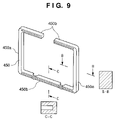
- FIG. 9 is a view showing details of the elastic member 450 .
- the elastic member 450 includes an arm portion 450 a extending in the expansion/contraction direction of the piezoelectric element 430 , and an arm portion 450 b extending in a direction perpendicular to the expansion/contraction direction.
- the arm portion 450 a and arm portion 450 b have different rigidities. That is, to allow the optical low-pass filter 410 to swing while following the expansion/contraction of the piezoelectric element 430 , the arm portion 450 b which receives an expansion/contraction action has a lower rigidity than the arm portion 450 a in the elastic member 450 . More specifically, the arm portion 450 a has a rectangular cross section B-B, while the arm portion 450 b has a cross section C-C with a partially hollow rectangular shape.
- arm portions formed from different members may be integrated by, e.g., coinjection molding.
- the piezoelectric element 430 and elastic member 450 seal the low-pass filter holding member 420 not to form any gap.
- the piezoelectric element 430 uses a stacked piezoelectric element in which generally known piezoelectric bodies and internal electrodes are alternately stacked.
- the piezoelectric element 430 also adopts a d 33 type stacked piezoelectric element which applies a voltage in the stacking direction of the piezoelectric body. This makes it possible to obtain a larger amplitude (displacement) in the stacking direction. That is, it is possible to largely displace the optical low-pass filter 410 in the vibration direction. It is also possible to use various other kinds of piezoelectric elements as long as the optical low-pass filter 410 is displaced in its in-plane direction, i.e., a direction perpendicular to the optical axis.
- the piezoelectric element 430 has a cross section perpendicular to its stacking direction (the vibration direction of the optical low-pass filter 410 ) with a dimension in the optical axis direction, which is almost equal to the thickness of the optical low-pass filter 410 .
- the cross section has a longer dimension in a direction perpendicular to the optical axis direction and vibration direction to increase the area of piezoelectric bodies to be stacked. This prevents an increase in dimension of the camera along the optical axis direction while attaining a larger force.
- Forming the piezoelectric element 430 to have the above-described cross section increases the allowable buckling stress with respect to its rotation within a plane perpendicular to the optical axis. This makes it possible to prevent the buckling fracture of the piezoelectric element even when the optical low-pass filter 410 vibrates with a rotational component within a plane perpendicular to the optical axis.
- the force F acting at the edge of the piezoelectric element changes depending on a dimension perpendicular to the expansion/contraction direction. Maximizing this dimension makes it possible to reduce the force acting at the edge of the piezoelectric element and to increase the allowable buckling stress by the moment M.
- the optical low-pass filter 410 directly abuts against the piezoelectric element 430 in the second embodiment, a spacer may be inserted between them.
- the piezoelectric element 430 needs only apply vibration to the spacer. This makes it possible to relax restriction on the layout.
- the optical low-pass filter 410 is allowed to incline with respect to a plane perpendicular to the image capturing optical axis, and the piezoelectric element 430 is bonded to the optical low-pass filter 410 , a shearing stress acts on the piezoelectric element 430 .
- the above arrangement is not preferable for a stacked piezoelectric element as in the second embodiment because it fractures due to such a shearing stress.
- the vibration surface of the piezoelectric element 430 with respect to the optical low-pass filter 410 is not bonded to the optical low-pass filter 410 but is merely in contact with it. Even when the optical low-pass filter 410 inclines with respect to a plane perpendicular to the image capturing optical axis, no shearing stress acts on the piezoelectric element 430 . That is, as the optical low-pass filter 410 inclines with respect to a plane perpendicular to the image capturing optical axis, the vibration surface of the piezoelectric element 430 relatively shifts from the contact surface of the optical low-pass filter 410 . The piezoelectric element 430 never directly receives the rotation force.
- the followability of the optical low-pass filter 410 with respect to the vibration of the piezoelectric element 430 suffers.
- this problem is dealt with by arranging the optical low-pass filter 410 to be clamped between the piezoelectric element 430 and the biasing member 440 within the same plane. That is, the optical low-pass filter 410 is biased using, e.g., a spring from the opposite side. This makes it possible to always bring the optical low-pass filter 410 into contact with the piezoelectric element 430 even when the piezoelectric element 430 is driven in the contraction direction.
- FIG. 11 is an exploded perspective view for further explaining the constituent components of the image capturing unit 400 described with reference to FIGS. 6 and 7 .
- Reference numeral 500 denotes an image sensor unit which includes at least the image sensor 33 and image sensor holding member 510 .
- Reference numeral 470 denotes the low-pass filter holding unit which includes at least the optical low-pass filter 410 , low-pass filter holding member 420 , piezoelectric element 430 , biasing member 440 , elastic member 450 , and a regulating member 460 .
- the regulating member 460 and low-pass filter holding member 420 clamps the optical low-pass filter 410 at predetermined gaps in the image capturing optical axis direction. This regulates the movement of the optical low-pass filter 410 in the image capturing optical axis direction. Such regulation prevents the optical low-pass filter 410 from inclining with respect to a plane perpendicular to the image capturing optical axis at a predetermined angle or more.
- the regulating member 460 also has an opening portion for regulating the opening of the optical low-pass filter 410 to shield the image capturing light beam which enters portions other than the opening portion. This prevents the image capturing light beam from entering the image sensor from the peripheral portion of the optical low-pass filter 410 so that the reflected light does not cause any ghost.
- Reference numeral 520 denotes the elastic rubber sheet.
- a stepped screw 530 locks the arm portion 420 b of the low-pass filter holding member 420 to the image sensor holding member 510 through the rubber sheet 520 to lock the low-pass filter holding unit 470 to the image sensor unit 500 .
- FIG. 12 is a view for explaining details of the rubber sheet 520 .
- the rubber sheet 520 is configured by integrally forming a frame portion 520 a and two arm portions 520 b .
- the two arm portions 520 b each have a support portion for supporting the stepped screw 530 and oppose each other.
- the surface of the frame portion 520 a on the image sensor 33 side is in tight contact with the image sensor holding member 510 , while the surface of the frame portion 520 a on the optical low-pass filter 410 side is in tight contact with the frame portion 420 a of the low-pass filter holding member 420 .
- the rubber sheet 520 seals the interval between the low-pass filter holding member 420 and the image sensor 33
- the piezoelectric element 430 and elastic member 450 seal the interval between the optical low-pass filter 410 and the low-pass filter holding member 420 .
- the space between the optical low-pass filter 410 and the image sensor 33 becomes an enclosed space for preventing the entrance of a foreign substance such as dirt.
- the present invention is not limited to this as long as the constituent component 520 is made of a member which has an airtightness high enough to prevent the entrance of a foreign substance, and a vibrational absorbability high enough not to conduct the vibration of the optical low-pass to the image sensor 33 .
- a member such as a gel sheet or a double-sided tape made of sponge having a predetermined thickness is applicable to the constituent component 520 .
- the rubber sheet 520 seals the interval between the low-pass filter holding member 420 and the image sensor 33 , while the piezoelectric element 430 and elastic member 450 seal the interval between the optical low-pass filter 410 and the low-pass filter holding member 420 .
- the space between the optical low-pass filter 410 and the image sensor 33 is an enclosed space free from any entrance of dirt or the like.
- the image sensor unit 500 and the low-pass filter holding unit 470 including, e.g., the optical low-pass filter 410 clamp the rubber sheet 520 .
- the rubber sheet 520 absorbs the vibration of the low-pass filter holding unit 470 .
- the vibration of the low-pass filter holding unit 470 is hardly conducted to the image sensor 33 .
- the vibration of the piezoelectric element 430 if any, hardly affects the image sensor 33 .
- the piezoelectric element 430 can be driven with smaller energy.
- the vibration of the optical low-pass filter 410 is hardly conducted to the image sensor 33 . This makes it possible to prevent damage such as bond removal of the image sensor 33 .
- an impact acts on the camera it is hardly conducted to the piezoelectric element 430 . This makes it possible to prevent the piezoelectric element 430 from being damaged upon an impact applied to the camera.
- the optical low-pass filter 410 and piezoelectric element 430 are not bonded, i.e., connected. Even when the piezoelectric element driving circuit 111 applies a predetermined cycle voltage to the piezoelectric element 430 to expand/contract it, a force in a direction in which the piezoelectric element 430 pushes out the optical low-pass filter 410 only acts on the piezoelectric element 430 , and no force in a direction in which the optical low-pass filter 410 pulls the piezoelectric element 430 acts on the piezoelectric element 430 by an inertia force. This makes it possible to prevent damage such as removal of a stacked portion because an excessive tensile force never acts on the piezoelectric element 430 even when a high-frequency voltage in an ultrasonic range is applied to the piezoelectric element 430 .
- the power supply is turned on via the main switch 43 in step S 1 to activate the camera in step S 2 . More specifically, the MPU 100 controls the power supply circuit 110 to supply power to each circuit, initializes the camera, and executes a camera ON operation which allows an image capturing operation.
- step S 3 It is determined in step S 3 whether the user has operated the cleaning instruction operation member 44 . If the user has operated the cleaning instruction operation member 44 (YES in step S 3 ), the process advances to step S 4 ; otherwise (NO in step S 3 ), the process advances to step S 5 .
- the power supply circuit 110 supplies power necessary for the cleaning mode to the units in the camera main body 1 as needed. Parallel to this operation, the remaining battery level of the power supply unit 42 is detected to transmit the detection result to the MPU 100 .
- the MPU 100 Upon receiving the cleaning mode start signal, the MPU 100 sends a driving signal to the piezoelectric element driving circuit 111 .
- the piezoelectric element driving circuit 111 Upon receiving the driving signal from the MPU 100 , the piezoelectric element driving circuit 111 generates a cycle voltage for driving the piezoelectric element 430 , and applies it to the piezoelectric element 430 .
- the piezoelectric element 430 expands/contracts in accordance with the applied voltage.
- the optical low-pass filter 410 moves in a direction perpendicular to the optical axis (in-plane direction) upon being pushed out by the piezoelectric element 430 , and the biasing member 440 contracts by the movement amount of the optical low-pass filter 410 .
- the optical low-pass filter 410 is biased against the piezoelectric element 430 by the biasing member 440 to move while following the contraction motion of the piezoelectric element 430 .
- the piezoelectric element driving circuit 111 applies a cycle voltage to the piezoelectric element 430 , the above-described motion repeats itself so that the optical low-pass filter 410 vibrates in a direction perpendicular to the optical axis, i.e., the in-plane direction while following cyclic expansion/contraction of the piezoelectric element 430 .
- step S 5 the process advances to step S 5 .
- the MPU 100 Upon receiving signals from the SW 1 7 a , SW 2 7 b , main operation dial 8 , sub operation dial 20 , image capture mode setting dial 14 , and other switches, the MPU 100 executes a camera operation such as image capture/setting of the camera in step S 5 . Since this operation is generally known, a detailed description thereof will be omitted.
- the piezoelectric element 430 may be driven by changing its parameters such as the driving frequency, driving time, and control method from those used in step S 4 in consideration of the power consumption and operation time of the camera.
- step S 8 the MPU 100 of the camera main body 1 controls to shut down each circuit, store necessary information and the like in the EEPROM 100 a , and control the power supply circuit 110 to execute a power OFF operation for shutting off power supply to desired circuits.
- the cleaning mode is executed to remove the foreign substance adhering on the optical low-pass filter 410 , not only at a timing intended by the user but also when the camera is powered off. Subsequently, the camera is powered off.
- Executing the cleaning mode at the power OFF operation timing after which the user leaves the camera unused for a long period of time at a high probability, makes it possible to more efficiently/effectively remove the foreign substance.
- This operation can be said to be more efficient/effective than foreign substance removal at the power ON operation timing before which the user has left the camera unused for a long period of time, and it has become hard to remove the dirt at a high probability.
- the power OFF operation timing does not indicate the power OFF moment, but implies a case in which the foreign substance is removed with a slight time lag from power OFF.
- the second embodiment has been described with reference to the case in which the foreign substance is removed upon the power OFF operation via the main switch 43 .
- the cleaning mode foreign substance removal
- the cleaning mode may be done at the timing for shifting to a sleep state in which power supply to the system is temporarily limited to save power.
- the description that the foreign substance is removed upon the power OFF operation via the main switch 43 indicates that the OFF operation signal from the main switch 43 is transmitted to the MPU 100 and the MPU 100 issues a command to cause the piezoelectric element driving circuit 111 to remove the foreign substance.
- the description that the cleaning mode is executed at the timing for shifting to a sleep state also indicates that the MPU 100 issues a command at the timing for shifting to a sleep state to cause the piezoelectric element driving circuit 111 to remove the foreign substance.
- FIGS. 14 and 15 Another form of the apparatus which removes a foreign substance adhering on an optical element such as an optical low-pass filter will be explained with reference to FIGS. 14 and 15 .
- An image capturing device 600 comprises an optical element 611 such as an optical low-pass filter, a holding member 612 for holding the optical element 611 , and a solid-state image capturing unit 613 which includes a solid-state image sensor 613 b and a cover member 613 a for protecting the solid-state image sensor 613 b .
- the image capturing device 600 also comprises a seal member 614 for sealing the interval between the optical element 611 and the cover member 613 a of the solid-state image capturing unit 613 .
- Reference numeral 621 denotes a lever which connects to a driving unit (not shown) and can travel in a direction indicated by an arrow D in FIG. 14 in parallel to the surface of the optical element 611 .
- the lever 621 comprises an abrasion-resistant fiber 622 (e.g., Dyneema manufactured by Toyobo Co. Ltd.).
- the abrasion-resistant fiber 622 serves as a cleaning brush.
- Reference numeral 623 denotes a foreign substance adhering on the optical element 611 .
- the abrasion-resistant fiber 622 has a length adjusted to come into contact with the optical element 611 .
- the operation in the cleaning mode is done at the camera power OFF operation timing. That is, executing the cleaning mode at the power OFF operation timing, after which the user leaves the camera unused for a long period of time at a high probability, makes it possible to more efficiently/effectively remove the foreign substance.
- FIGS. 16 and 17 Another form of the apparatus which removes a foreign substance adhering on an optical element such as an optical low-pass filter will be explained with reference to FIGS. 16 and 17 .
- Reference numeral 721 denotes an insulating portion which is made of polyimide and can travel in a direction indicated by an arrow E in FIG. 16 in parallel to the surface of the optical element 711 .
- a coil (not shown) can switch the insulating portion 721 between a charged state and a charge-removed state.
- Reference numeral 723 denotes a foreign substance adhering on the optical element 711 .
- the insulating portion 721 is positioned at the upper portion of FIG. 16 . As the operation in the cleaning mode starts, a predetermined voltage is applied to the coil (not shown). The insulating portion 721 is charged and travels downward.
- the insulating portion 721 As the insulating portion 721 is charged, if the charged foreign substance 723 is adhering to the surface of the optical element 711 , the charged foreign substance 723 and insulating portion 721 produce an electrostatic force between themselves. The insulating portion 721 attracts by the electrostatic force (electrostatic attraction force) the foreign substance 723 against its adhesion force acting on the surface of the optical element 711 . The foreign substance 723 attracted to the insulating portion 721 by the electrostatic force remains on the surface of the insulating portion 721 . When the insulating portion 721 completes downward travel, the coil (not shown) applies, to the insulating portion 721 , a voltage having a charge opposite to that applied in charging.
- the electrostatic force electrostatic attraction force
- the insulating portion 721 is then charge-removed. With this charge removing operation, the foreign substance 723 adhering to the surface of the insulating portion 721 by the electrostatic force separates and falls from the surface of the insulating portion 721 by gravity.
- the insulating portion 721 After that, the insulating portion 721 returns to the upward original position.
- the operation in the cleaning mode is done at the camera power OFF operation timing. That is, executing the cleaning mode at the power OFF operation timing, after which the user leaves the camera unused for a long period of time at a high probability, makes it possible to more efficiently/effectively remove the foreign substance.
- a storage medium (or recording medium) which records software program codes for implementing the functions of the above-described embodiments is supplied to the system or apparatus.
- the computer or CPU or MPU
- the program codes read out from the storage medium implement the functions of the above-described embodiments by themselves, and the storage medium which stores the program codes constitutes the present invention.
- the present invention incorporates the following case. That is, the functions of the above-described embodiments are implemented when the operating system (OS) running on the computer performs part or all of actual processing on the basis of the instructions of the program codes.
- the present invention also incorporates the following case. That is, the program codes read out from the storage medium are written in the memory of a function expansion card inserted into the computer or a function expansion unit connected to the computer. After that, the functions of the above-described embodiments are implemented when the CPU of the function expansion card or function expansion unit performs part or all of actual processing on the basis of the instructions of the program codes.
- the storage medium stores program codes corresponding to the above-described procedures.
Landscapes
- Physics & Mathematics (AREA)
- General Physics & Mathematics (AREA)
- Engineering & Computer Science (AREA)
- Multimedia (AREA)
- Signal Processing (AREA)
- Optics & Photonics (AREA)
- Studio Devices (AREA)
- Camera Bodies And Camera Details Or Accessories (AREA)
- Blocking Light For Cameras (AREA)
Abstract
Description
force F=M/(L/2)
Claims (7)
Applications Claiming Priority (7)
| Application Number | Priority Date | Filing Date | Title |
|---|---|---|---|
| JP2006-063978(PAT.) | 2006-03-09 | ||
| JP2006063978 | 2006-03-09 | ||
| JP2006-063978 | 2006-03-09 | ||
| JP2006-198709(PAT.) | 2006-07-20 | ||
| JP2006-198709 | 2006-07-20 | ||
| JP2006198709A JP4702954B2 (en) | 2006-03-09 | 2006-07-20 | Imaging device |
| PCT/JP2007/053999 WO2007105502A1 (en) | 2006-03-09 | 2007-03-02 | Imaging device, and method and program for controlling same |
Related Parent Applications (1)
| Application Number | Title | Priority Date | Filing Date |
|---|---|---|---|
| PCT/JP2007/053999 Continuation WO2007105502A1 (en) | 2006-03-09 | 2007-03-02 | Imaging device, and method and program for controlling same |
Publications (2)
| Publication Number | Publication Date |
|---|---|
| US20070211162A1 US20070211162A1 (en) | 2007-09-13 |
| US7719600B2 true US7719600B2 (en) | 2010-05-18 |
Family
ID=38478529
Family Applications (1)
| Application Number | Title | Priority Date | Filing Date |
|---|---|---|---|
| US11/739,394 Expired - Fee Related US7719600B2 (en) | 2006-03-09 | 2007-04-24 | Image capturing apparatus, control method therefor, and program regarding foreign substance removal |
Country Status (7)
| Country | Link |
|---|---|
| US (1) | US7719600B2 (en) |
| EP (1) | EP1874042B1 (en) |
| JP (1) | JP4702954B2 (en) |
| KR (1) | KR100918809B1 (en) |
| CN (1) | CN101326813B (en) |
| DE (1) | DE602007011356D1 (en) |
| WO (1) | WO2007105502A1 (en) |
Cited By (6)
| Publication number | Priority date | Publication date | Assignee | Title |
|---|---|---|---|---|
| US20080198458A1 (en) * | 2007-02-20 | 2008-08-21 | Canon Kabushiki Kaisha | Image capturing apparatus |
| US20100045832A1 (en) * | 2008-08-19 | 2010-02-25 | Canon Kabushiki Kaisha | Manufacturing method of solid-state imaging apparatus, solid-state imaging apparatus, and electronic imaging apparatus |
| US20100165187A1 (en) * | 2008-12-26 | 2010-07-01 | Takashi Miyazawa | Vibrating device and image equipment having the same |
| US20100165121A1 (en) * | 2008-12-26 | 2010-07-01 | Sumio Kawai | Vibrating device and image equipment having the same |
| US20100165186A1 (en) * | 2008-12-26 | 2010-07-01 | Sumio Kawai | Vibrating device and image equipment having the same |
| US20100165170A1 (en) * | 2008-12-26 | 2010-07-01 | Sumio Kawai | Vibrating device and image equipment having the same |
Families Citing this family (17)
| Publication number | Priority date | Publication date | Assignee | Title |
|---|---|---|---|---|
| JP4819575B2 (en) * | 2006-05-26 | 2011-11-24 | キヤノン株式会社 | Imaging device |
| JP4804251B2 (en) * | 2006-07-20 | 2011-11-02 | キヤノン株式会社 | Imaging device and imaging unit |
| US8514316B2 (en) | 2007-10-25 | 2013-08-20 | Nikon Corporation | Image device and optical device for providing dust removing capabilities |
| JP5233586B2 (en) * | 2007-10-26 | 2013-07-10 | 株式会社ニコン | Imaging apparatus, optical apparatus, and manufacturing method of imaging apparatus |
| JP5344134B2 (en) * | 2007-10-31 | 2013-11-20 | 株式会社ニコン | Imaging device and optical device |
| JP5121443B2 (en) * | 2007-12-28 | 2013-01-16 | キヤノン株式会社 | Imaging device and optical filter |
| JP5262135B2 (en) * | 2008-01-28 | 2013-08-14 | 株式会社ニコン | Optical components and optical equipment |
| KR20110092545A (en) * | 2010-02-09 | 2011-08-18 | 삼성전자주식회사 | Imaging device |
| JP5762034B2 (en) * | 2011-02-09 | 2015-08-12 | キヤノン株式会社 | Foreign object removal unit and optical apparatus provided with the same |
| CN103312948A (en) * | 2012-03-12 | 2013-09-18 | 华晶科技股份有限公司 | Camera device and vibration dust removal method thereof |
| KR101920723B1 (en) | 2012-12-10 | 2019-02-14 | 삼성전자주식회사 | Piezoelectric liner actuator |
| JP2016024383A (en) * | 2014-07-22 | 2016-02-08 | ソニー株式会社 | Electronic device |
| US9602730B2 (en) * | 2014-12-31 | 2017-03-21 | Torrey Pines Logic, Inc. | Mountable, thermal situational-awareness accessory for use with optical devices |
| CN110574358B (en) * | 2017-04-26 | 2021-05-28 | 株式会社村田制作所 | Cleaning device and imaging unit provided with same |
| US11143933B2 (en) * | 2019-01-08 | 2021-10-12 | Funder Electronic Global Co., Ltd. | Camera assembly |
| CN111835956B (en) * | 2019-04-16 | 2022-07-12 | 北京地平线机器人技术研发有限公司 | Camera control method and device, image acquisition equipment and electronic equipment |
| JP2023073022A (en) | 2021-11-15 | 2023-05-25 | キヤノン株式会社 | Imaging apparatus |
Citations (13)
| Publication number | Priority date | Publication date | Assignee | Title |
|---|---|---|---|---|
| JPH09200591A (en) | 1996-01-17 | 1997-07-31 | Canon Inc | Video camera equipment |
| JP2002204379A (en) | 2000-12-28 | 2002-07-19 | Olympus Optical Co Ltd | Camera |
| CN1448776A (en) | 2002-04-03 | 2003-10-15 | 佳能株式会社 | Photographic device, action processing method, program and storage medium |
| US20030202114A1 (en) * | 2002-04-26 | 2003-10-30 | Olympus Optical Co., Ltd. | Camera and image pickup device unit used therein |
| JP2003330082A (en) | 2002-05-17 | 2003-11-19 | Olympus Optical Co Ltd | Electronic imaging device |
| US20040047625A1 (en) | 2002-05-17 | 2004-03-11 | Junichi Ito | Electronic imaging apparatus with anti-dust function |
| JP2004184949A (en) | 2002-12-06 | 2004-07-02 | Nikon Corp | Camera |
| JP2004264580A (en) | 2003-02-28 | 2004-09-24 | Olympus Corp | Electronic imaging apparatus |
| US6895368B2 (en) * | 2001-12-12 | 2005-05-17 | Konica Corporation | Maintenance information supply system with a host computer and an electronic device |
| US20050104997A1 (en) * | 2003-11-17 | 2005-05-19 | Osamu Nonaka | Lens replacement type imaging apparatus, control apparatus, cleaning apparatus, and cleaning method |
| JP2005159711A (en) | 2003-11-26 | 2005-06-16 | Konica Minolta Photo Imaging Inc | Imaging apparatus |
| JP2006060428A (en) | 2004-08-18 | 2006-03-02 | Fuji Photo Film Co Ltd | Electronic camera |
| US7215372B2 (en) * | 2002-05-17 | 2007-05-08 | Olympus Corporation | Optical apparatus having dust off function |
-
2006
- 2006-07-20 JP JP2006198709A patent/JP4702954B2/en not_active Expired - Fee Related
-
2007
- 2007-03-02 WO PCT/JP2007/053999 patent/WO2007105502A1/en active Application Filing
- 2007-03-02 CN CN2007800006383A patent/CN101326813B/en not_active Expired - Fee Related
- 2007-03-02 EP EP07737647A patent/EP1874042B1/en not_active Not-in-force
- 2007-03-02 KR KR1020077027790A patent/KR100918809B1/en not_active Expired - Fee Related
- 2007-03-02 DE DE602007011356T patent/DE602007011356D1/en active Active
- 2007-04-24 US US11/739,394 patent/US7719600B2/en not_active Expired - Fee Related
Patent Citations (16)
| Publication number | Priority date | Publication date | Assignee | Title |
|---|---|---|---|---|
| JPH09200591A (en) | 1996-01-17 | 1997-07-31 | Canon Inc | Video camera equipment |
| JP2002204379A (en) | 2000-12-28 | 2002-07-19 | Olympus Optical Co Ltd | Camera |
| US6895368B2 (en) * | 2001-12-12 | 2005-05-17 | Konica Corporation | Maintenance information supply system with a host computer and an electronic device |
| CN1448776A (en) | 2002-04-03 | 2003-10-15 | 佳能株式会社 | Photographic device, action processing method, program and storage medium |
| US20040017480A1 (en) * | 2002-04-03 | 2004-01-29 | Masaki Higashihara | Image pickup apparatus, operation processing method therefor, program for implementing the method, and storage medium storing the program |
| US7349014B2 (en) * | 2002-04-03 | 2008-03-25 | Canon Kabushiki Kaisha | Image pickup apparatus, operation processing method therefor, program for implementing the method, and storage medium storing the program |
| US20030202114A1 (en) * | 2002-04-26 | 2003-10-30 | Olympus Optical Co., Ltd. | Camera and image pickup device unit used therein |
| US7324148B2 (en) * | 2002-04-26 | 2008-01-29 | Olympus Optical Co., Ltd. | Camera and image pickup device unit used therefor having a sealing structure between a dust proofing member and an image pick up device |
| US7215372B2 (en) * | 2002-05-17 | 2007-05-08 | Olympus Corporation | Optical apparatus having dust off function |
| JP2003330082A (en) | 2002-05-17 | 2003-11-19 | Olympus Optical Co Ltd | Electronic imaging device |
| US20040047625A1 (en) | 2002-05-17 | 2004-03-11 | Junichi Ito | Electronic imaging apparatus with anti-dust function |
| JP2004184949A (en) | 2002-12-06 | 2004-07-02 | Nikon Corp | Camera |
| JP2004264580A (en) | 2003-02-28 | 2004-09-24 | Olympus Corp | Electronic imaging apparatus |
| US20050104997A1 (en) * | 2003-11-17 | 2005-05-19 | Osamu Nonaka | Lens replacement type imaging apparatus, control apparatus, cleaning apparatus, and cleaning method |
| JP2005159711A (en) | 2003-11-26 | 2005-06-16 | Konica Minolta Photo Imaging Inc | Imaging apparatus |
| JP2006060428A (en) | 2004-08-18 | 2006-03-02 | Fuji Photo Film Co Ltd | Electronic camera |
Non-Patent Citations (4)
| Title |
|---|
| PCT/IB/338, PCT/IB/373, PCT/ISA/237, and PCT/ISA/210 which comprise an English translation of Form PCT/ISA/237 (International Preliminary Report on Patentability for PCT/JP2007/053999) submitted to the USPTO on May 30, 2007. |
| The above reference was cited in a Apr. 7, 2009 Japanese Office Action that issued in Japanese Patent Application No. 2006-159784. |
| The above reference was cited in a Feb. 10, 2010 European Search Report of the counterpart European Patent Application No. 07737647.3, a copy of which is not enclosed. |
| The above references were cited in a Dec. 11, 2009 Chinese Office Action that issued in Chinese Patent Application No. 200780000638.3, a copy of which is enclosed with English Translation. |
Cited By (15)
| Publication number | Priority date | Publication date | Assignee | Title |
|---|---|---|---|---|
| US20120182457A1 (en) * | 2007-02-20 | 2012-07-19 | Canon Kabushiki Kaisha | Image capturing apparatus |
| US20080198458A1 (en) * | 2007-02-20 | 2008-08-21 | Canon Kabushiki Kaisha | Image capturing apparatus |
| US8480240B2 (en) * | 2007-02-20 | 2013-07-09 | Canon Kabushiki Kaisha | Image capturing apparatus |
| US8136952B2 (en) * | 2007-02-20 | 2012-03-20 | Canon Kabushiki Kaisha | Image capturing apparatus |
| US20100045832A1 (en) * | 2008-08-19 | 2010-02-25 | Canon Kabushiki Kaisha | Manufacturing method of solid-state imaging apparatus, solid-state imaging apparatus, and electronic imaging apparatus |
| US9111827B2 (en) | 2008-08-19 | 2015-08-18 | Canon Kabushiki Kaisha | Manufacturing method of solid-state imaging apparatus, solid-state imaging apparatus, and electronic imaging apparatus |
| US8643773B2 (en) * | 2008-08-19 | 2014-02-04 | Canon Kabushiki Kaisha | Manufacturing method of solid-state imaging apparatus, solid-state imaging apparatus, and electronic imaging apparatus |
| US20100165121A1 (en) * | 2008-12-26 | 2010-07-01 | Sumio Kawai | Vibrating device and image equipment having the same |
| US8164634B2 (en) * | 2008-12-26 | 2012-04-24 | Olympus Corporation | Vibrating device and image equipment having the same |
| US8253838B2 (en) * | 2008-12-26 | 2012-08-28 | Olympus Imaging Corp. | Vibrating device and image equipment having the same |
| US8253853B2 (en) * | 2008-12-26 | 2012-08-28 | Olympus Corporation | Vibrating device and image equipment having the same |
| US8339510B2 (en) * | 2008-12-26 | 2012-12-25 | Olympus Corporation | Vibrating device and image equipment having the same |
| US20100165170A1 (en) * | 2008-12-26 | 2010-07-01 | Sumio Kawai | Vibrating device and image equipment having the same |
| US20100165186A1 (en) * | 2008-12-26 | 2010-07-01 | Sumio Kawai | Vibrating device and image equipment having the same |
| US20100165187A1 (en) * | 2008-12-26 | 2010-07-01 | Takashi Miyazawa | Vibrating device and image equipment having the same |
Also Published As
| Publication number | Publication date |
|---|---|
| KR20080009303A (en) | 2008-01-28 |
| CN101326813B (en) | 2011-09-14 |
| US20070211162A1 (en) | 2007-09-13 |
| JP4702954B2 (en) | 2011-06-15 |
| KR100918809B1 (en) | 2009-09-25 |
| EP1874042A4 (en) | 2010-03-10 |
| WO2007105502A1 (en) | 2007-09-20 |
| JP2007274663A (en) | 2007-10-18 |
| DE602007011356D1 (en) | 2011-02-03 |
| EP1874042B1 (en) | 2010-12-22 |
| EP1874042A1 (en) | 2008-01-02 |
| CN101326813A (en) | 2008-12-17 |
Similar Documents
| Publication | Publication Date | Title |
|---|---|---|
| US7719600B2 (en) | Image capturing apparatus, control method therefor, and program regarding foreign substance removal | |
| KR100769614B1 (en) | Image pickup apparatus with foreign object removal capabilities | |
| CN101937131B (en) | Vibrating device and image equipment having the same | |
| US7978220B2 (en) | Optical apparatus having device for removing foreign substance | |
| US8159603B2 (en) | Image capturing apparatus with frame for sealing between optical member and image sensor | |
| JP5901347B2 (en) | Imaging device | |
| US7969500B2 (en) | Optical apparatus having device for removing foreign substance | |
| JP2004032191A (en) | Electronic imaging device | |
| JP6460824B2 (en) | Optical apparatus and control method thereof | |
| JP5484077B2 (en) | Imaging unit and imaging apparatus | |
| JP2008236669A (en) | IMAGING DEVICE, ITS CONTROL METHOD, PROGRAM, AND STORAGE MEDIUM | |
| JP5264302B2 (en) | Imaging device | |
| JP5484084B2 (en) | Imaging unit and imaging apparatus | |
| JP5159198B2 (en) | Imaging device | |
| JP2008028615A (en) | Imaging device | |
| JP5283837B2 (en) | Optical equipment | |
| JP2011061382A (en) | Imaging unit and imaging apparatus | |
| JP2008026530A (en) | Imaging device | |
| JP2009267536A (en) | Imaging device | |
| JP2007134802A (en) | Imaging device | |
| JP2003338967A (en) | Camera and imaging element unit | |
| JP2015126420A (en) | Imaging apparatus, control method and program thereof | |
| JP2007134801A (en) | Imaging device |
Legal Events
| Date | Code | Title | Description |
|---|---|---|---|
| AS | Assignment |
Owner name: CANON KABUSHIKI KAISHA,JAPAN Free format text: ASSIGNMENT OF ASSIGNORS INTEREST;ASSIGNORS:KAIHARA, SHOJI;KATAYAMA, ATSUSHI;REEL/FRAME:019203/0443 Effective date: 20070410 Owner name: CANON KABUSHIKI KAISHA, JAPAN Free format text: ASSIGNMENT OF ASSIGNORS INTEREST;ASSIGNORS:KAIHARA, SHOJI;KATAYAMA, ATSUSHI;REEL/FRAME:019203/0443 Effective date: 20070410 |
|
| STCF | Information on status: patent grant |
Free format text: PATENTED CASE |
|
| FEPP | Fee payment procedure |
Free format text: PAYOR NUMBER ASSIGNED (ORIGINAL EVENT CODE: ASPN); ENTITY STATUS OF PATENT OWNER: LARGE ENTITY |
|
| FPAY | Fee payment |
Year of fee payment: 4 |
|
| MAFP | Maintenance fee payment |
Free format text: PAYMENT OF MAINTENANCE FEE, 8TH YEAR, LARGE ENTITY (ORIGINAL EVENT CODE: M1552) Year of fee payment: 8 |
|
| FEPP | Fee payment procedure |
Free format text: MAINTENANCE FEE REMINDER MAILED (ORIGINAL EVENT CODE: REM.); ENTITY STATUS OF PATENT OWNER: LARGE ENTITY |
|
| LAPS | Lapse for failure to pay maintenance fees |
Free format text: PATENT EXPIRED FOR FAILURE TO PAY MAINTENANCE FEES (ORIGINAL EVENT CODE: EXP.); ENTITY STATUS OF PATENT OWNER: LARGE ENTITY |
|
| STCH | Information on status: patent discontinuation |
Free format text: PATENT EXPIRED DUE TO NONPAYMENT OF MAINTENANCE FEES UNDER 37 CFR 1.362 |
|
| FP | Lapsed due to failure to pay maintenance fee |
Effective date: 20220518 |