US7692306B2 - Semiconductor device - Google Patents
Semiconductor device Download PDFInfo
- Publication number
- US7692306B2 US7692306B2 US11/785,653 US78565307A US7692306B2 US 7692306 B2 US7692306 B2 US 7692306B2 US 78565307 A US78565307 A US 78565307A US 7692306 B2 US7692306 B2 US 7692306B2
- Authority
- US
- United States
- Prior art keywords
- interconnect
- semiconductor device
- interconnects
- substrate
- layer
- Prior art date
- Legal status (The legal status is an assumption and is not a legal conclusion. Google has not performed a legal analysis and makes no representation as to the accuracy of the status listed.)
- Expired - Fee Related
Links
Images


Classifications
-
- H—ELECTRICITY
- H01—ELECTRIC ELEMENTS
- H01L—SEMICONDUCTOR DEVICES NOT COVERED BY CLASS H10
- H01L21/00—Processes or apparatus adapted for the manufacture or treatment of semiconductor or solid state devices or of parts thereof
- H01L21/70—Manufacture or treatment of devices consisting of a plurality of solid state components formed in or on a common substrate or of parts thereof; Manufacture of integrated circuit devices or of parts thereof
- H01L21/71—Manufacture of specific parts of devices defined in group H01L21/70
- H01L21/768—Applying interconnections to be used for carrying current between separate components within a device comprising conductors and dielectrics
- H01L21/76838—Applying interconnections to be used for carrying current between separate components within a device comprising conductors and dielectrics characterised by the formation and the after-treatment of the conductors
-
- H—ELECTRICITY
- H01—ELECTRIC ELEMENTS
- H01L—SEMICONDUCTOR DEVICES NOT COVERED BY CLASS H10
- H01L21/00—Processes or apparatus adapted for the manufacture or treatment of semiconductor or solid state devices or of parts thereof
- H01L21/70—Manufacture or treatment of devices consisting of a plurality of solid state components formed in or on a common substrate or of parts thereof; Manufacture of integrated circuit devices or of parts thereof
- H01L21/71—Manufacture of specific parts of devices defined in group H01L21/70
- H01L21/768—Applying interconnections to be used for carrying current between separate components within a device comprising conductors and dielectrics
- H01L21/76801—Applying interconnections to be used for carrying current between separate components within a device comprising conductors and dielectrics characterised by the formation and the after-treatment of the dielectrics, e.g. smoothing
- H01L21/76802—Applying interconnections to be used for carrying current between separate components within a device comprising conductors and dielectrics characterised by the formation and the after-treatment of the dielectrics, e.g. smoothing by forming openings in dielectrics
- H01L21/76816—Aspects relating to the layout of the pattern or to the size of vias or trenches
Definitions
- the present invention relates to a semiconductor device.
- a typical test pattern utilized for an evaluating a process for a semiconductor device will be described.
- a general view of a layout of a test chip for a general process evaluation is shown in FIG. 8 .
- Maximum values of a horizontal width d 1 and a vertical width d 2 in a dimension of a test chip are generally defined by employing a maximum field size of a lithographic apparatus.
- An evaluation pattern is composed of an assembly of evaluation blocks, which are also called as sub chips 803 .
- the dimensions of the sub chips 803 are constant in the interior of the testing block. The reason thereof is that this leads to a fixed arrangement of measuring probes and a constant moving distances thereof in a program for measurement, thereby allowing a sharing of a program and a common use of measurement probes.
- the pattern for evaluating the interconnect process includes via chains, a pattern for evaluating electro migration (EM), a pattern for measuring a leakage or the like, which are mounted therein.
- EM electro migration
- a pattern scaling is generally changed according to the length of the interconnect to be evaluated and the number of vias.
- a defect density can also be evaluated by utilizing different pattern scales.
- test element group (TEG) region 901 An evaluation block required for such process evaluation is referred to as test element group (TEG) region 901 , and the electrode that a probe for electrical measurement lets come into contact is called electrode pad 902 , and an interconnect that couples the TEG region 901 to the electrode pad 902 is referred to as a drawing interconnect 903 .
- TEG test element group
- FIG. 10 is a plan view, which includes a via chain pattern TEG region 1001 and drawing interconnects 1002 , which electrically couples the region 1001 is to the electrode pads. Portions of the drawing interconnects 1002 coupled to via chain pattern TEG region 1001 are formed to have a linewidth that is larger than a linewidth of the interconnect in the region 1001 .
- M 1 interconnects 1003 and M 2 interconnects 1004 are alternately disposed, and these interconnects are mutually coupled by vias 1005 . Meanwhile, linewidths d 3 of the M 1 interconnect 1003 and the M 2 interconnect 1004 are 70 nm, which is equivalent to a minimum linewidth in the semiconductor device.
- turning back M 1 interconnects 1006 are provided. Meanwhile, the turning back region has an interconnect data rate of 75% over a minimum normalization area (140 nm ⁇ 140 nm), which is area of a region 1008 that is composed of four grids having of a square having a side, which is equivalent to a minimum interconnect interval of repeated data. This is because the turning back region stores data in three grids of the above-described four grids.
- a minimum normalization area 140 nm ⁇ 140 nm
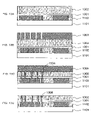
- FIGS. 11A to 11C , FIGS. 12A to 12D , FIGS. 13A to 13D and FIGS. 14A to 14C are cross-sectional views, illustrating the process. These cross-sectional views represent cross sections along dotted line L 1 in FIG. 10 .
- an interlayer insulating film 1102 composed of silicon oxide film or the like is formed on a substrate 1101 via a chemical vapor deposition (CVD) process or the like ( FIG. 11A ).
- CVD chemical vapor deposition
- a resist 1103 is formed on the interlayer insulating film 1102 , and the formed resist 1103 is patterned via a photolithographic process. Further, a pattern of the resist is transferred to the interlayer insulating film 1102 via a dry etch technology to form trenches 1104 for interconnects in desired positions ( FIG. 11B ). Then, the remained resist 1103 is removed ( FIG. 1C ).
- a resist 1201 is formed on the interlayer insulating film 1102 , and the formed resist 1201 is patterned via a photolithographic process ( FIG. 12A ). Further, a pattern of the resist is transferred to the interlayer insulating film 1102 via a dry etch technology to form trenches 1202 for interconnects in desired positions. Then, the remained resist 1201 is removed ( FIG. 12B ). Subsequently, a conductor film 1203 such as a copper (Cu) film, an aluminum (Al) film and the like is deposited on the entire surface of the interlayer insulating film 1102 ( FIG. 12C ).
- a conductor film 1203 such as a copper (Cu) film, an aluminum (Al) film and the like is deposited on the entire surface of the interlayer insulating film 1102 ( FIG. 12C ).
- the conductor film 1203 is polished via a chemical mechanical polishing (CMP) process until the interlayer insulating film 1102 is exposed.
- CMP chemical mechanical polishing
- a diffusion barrier film 1301 composed of a silicon carbide (SiC) film or the like is formed on the interlayer insulating film 1102 having the interconnect 1204 formed thereon, and then, an interlayer insulating film 1302 composed of a silicon oxide film or the like is formed thereon ( FIG. 13A ).
- a resist 1303 is formed on the interlayer insulating film 1302 , and the formed resist 1303 is patterned via a photolithographic process ( FIG. 13B ). Further, a pattern of the resist is transferred to the interlayer insulating film 1302 via a dry etch technology to form trenches 1304 for interconnects in desired positions. Then, the remained resist 1303 is removed.
- a conductor film 1305 such as a Cu film, an Al film and the like is deposited on the entire surface of the interlayer insulating film 1302 ( FIG. 13C ). Then, the conductor film 1305 is polished via a CMP process until the interlayer insulating film 1302 is exposed. As a result, vias 1306 are formed in desired locations of the interlayer insulating film 1302 ( FIG. 13D ).
- a diffusion barrier film 1401 composed of a SiC film or the like is formed on the interlayer insulating film 1302 having the vias 1306 formed thereon, and then, an interlayer insulating film 1402 composed of a silicon oxide film or the like is formed thereon ( FIG. 14A ).
- a resist is formed on the interlayer insulating film 1402 , and the formed resist is patterned via a photolithographic process. Further, a pattern of the resist is transferred to the interlayer insulating film 1402 via a dry etch technology to form trenches 1403 for interconnects in desired positions. Then, the remained resist is removed ( FIG. 14B ).
- a conductor film such as a Cu film, an Al film and the like is deposited on the entire surface of the interlayer insulating film 1402 . Then, the conductor film is polished via a CMP process until the interlayer insulating film 1402 is exposed. As a result, an interconnect 1404 having a damascene structure is formed in a desired location of the interlayer insulating film 1402 ( FIG. 14C ).
- a structure of a coupling interconnect from a certain isolated block to an electric block in electrically dense blocks is not limited to a TEG drawing interconnect for evaluating the process, and a similar structure is employed for the product. Therefore, a typical conventional product thereof will be described as follows.
- FIG. 15 is a plan view, showing an outline of a general logic product.
- This product has four macro-functions, namely an input-output (I/O) block 1501 , a random access memory (RAM) block 1502 , a logic block 1503 and a phase locked loop (PLL) block 1504 .
- I/O input-output
- RAM random access memory
- PLL phase locked loop
- the I/O block 1501 is an area composed of only interconnects having the linewidth of not smaller than 1 ⁇ m. In such area, there is basically no need for a narrower interconnect. Further, this area serves as determining a limitation on an allowable high-current, and maximum values of the linewidth and the via dimension are determined by such area.
- An interconnect that couples the circuit blocks in the I/O block is composed of two interconnects, namely an interconnect that is coupled to a pad electrode (input interconnect) and an interconnect that is coupled to an internal circuit (output interconnect).
- the RAM block 1502 generally includes a memory device of around 1 MB. A priority is given to a miniaturization for the interconnects in such area over an operating speed. Therefore, this area is an area of highest need for narrower interconnects. Relatively few large interconnects are included in this area, and power supply interconnects and ground interconnects are alternately disposed with a pitch of a memory cell size.
- the logic block 1503 is a cell, in which higher drive capacity is required, and is also a block, in which power supply interconnects are enhanced.
- a configuration of this area is basically similar to a configuration of a standard cell of a gate array.
- the configuration of this area related to the interconnects generally includes enhanced power supply interconnects as compared with that of the RAM, though it is similar to that of RAM.
- a plurality of couplings between macro circuits are generally included, unlikely in the case of the PLL.
- the PLL block 1504 Since stable operations of the power supply, the ground and the capacitor element are prioritized in the PLL block 1504 , the PLL block 1504 generally requires second largest linewidth, second only to the I/O region, though the interconnect density therein is lower.
- the PLL serves as amplifying a signal input from an external transmitter (amplifying a signal to, for example, in 4 times or 5 times of the original), so as to compose clock trees in respective macros.
- a clock input section and a clock output section in this clock serves as drawing interconnects from the macro circuit. Only two input and output interconnects are basically present in the PLL.
- a block coupling structure of two macro circuits in a logic unit will be described in reference to FIG. 16 .
- a region between two macro circuits of a first logic region 1601 and a second logic region 1602 is a region 1603 .
- Power supply meshes 1604 and ground meshes 1605 are disposed in the macro.
- Connections and signal interconnects 1606 serving as a circuit structure factor are disposed between the power supply meshes 1604 and the ground meshes 1605 in the macro. Further, signal interconnects for connecting these macros are drawn.
- a region for preparing a coupling of the signal interconnects is a region 1607 .
- the macros may be mutually coupled in the same interconnect layer or may be mutually coupled in different interconnect layers.
- FIG. 17 shows a logic unit 1701 and a macro coupling region 1702 .
- a portion of the interconnect 1703 has a linewidth that is wider than a linewidth of the interconnect in the macro in the macro coupling region 1702 .
- the interconnect 1703 is coupled to a M 2 interconnect 1708 through via 1707 within the macro.
- the power supply interconnects 1704 and the ground interconnects 1705 are alternately disposed.
- the signal interconnects 1706 are disposed between the power supply interconnects 1704 and ground interconnects 1705 . Further, it is common that the signal interconnect 1706 is arranged to be in parallel with x direction (transverse direction in the diagram) and with y direction (longitudinal direction in the diagram).
- a region of larger data rate causes a varied level of the light exposure in the lithographic operation in the process for manufacturing the semiconductor device, causing a problem of allowing narrower process window.
- the narrower process window may cause, for example, a break in the end of the macro coupling region, leading to a short circuit.
- Optimum level of light exposure in the lithographic process is decreased as the data rate is increased. This is resulted from a flare phenomenon, namely a phenomenon that a blurring is caused in a pattern image by an irregular reflection of a beam through a lens. This phenomenon is characterized that the pattern geometry is changed depending on the data rate. Therefore, in order to inhibiting such phenomenon, it is required to provide a limitation in a range of the available interconnect data rate.
- a semiconductor device having an interconnect layer provided on a substrate, comprising: a first interconnect, provided in the interconnect layer, and elongating along a first direction included in a substrate surface of the substrate; a second interconnect, provided in the interconnect layer, elongating along the first interconnect, and being spaced apart from the first interconnect in plan view; and a slit-shaped via plug, provided in the interconnect layer, elongating along a second direction, which is a direction being normal to the first direction and is included in the substrate surface of the substrate, and being capable of electrically coupling the first interconnect to the second interconnect.
- an electrical coupling between the first interconnect and the second interconnect is provided by employing a slit-shaped via plug that elongates along a direction normal to these elongation directions.
- This configuration provides a reduced interconnect data rate generated in a turning back region of the interconnect.
- a semiconductor device which is capable of providing a reduced interconnect data rate generated in a turning back region of the interconnect, can be achieved.
- FIG. 1 is a plan view, showing an example of a semiconductor device according to the present invention
- FIGS. 2A to 2C are cross-sectional views of the semiconductor device, which are helpful in describing a method for manufacturing the semiconductor device of FIG. 1 ;
- FIGS. 3A to 3D are cross-sectional views of the semiconductor device, which are helpful in describing a method for manufacturing the semiconductor device of FIG. 1 ;
- FIGS. 4A to 4D are cross-sectional views of the semiconductor device, which are helpful in describing a method for manufacturing the semiconductor device of FIG. 1 ;
- FIGS. 5A to 5C are cross-sectional views of the semiconductor device, which are helpful in describing a method for manufacturing the semiconductor device of FIG. 1 ;
- FIG. 6 is a plan view of a semiconductor device, helpful in describing an exemplary implementation, in which the present invention applied to a general logic circuit;
- FIG. 7 is a graph, showing experimental results for confirming the advantageous effect of the present invention, in which ordinate represents frequencies of failure generation for 50,000 of series via chains, and abscissa represents lengths (extension length) of interconnect data added from the via end;
- FIG. 8 is a plan view, showing a layout of a general test chip for evaluating process
- FIG. 9 is a plan view, which is helpful in describing an outline of a pattern for evaluating the interconnect process
- FIG. 10 is a plan view, showing a region for coupling the TEG region with the electrode pad
- FIGS. 11A to 11C are cross-sectional views, which are helpful in describing a general process for forming a dual-layered interconnect
- FIGS. 12A to 12D are cross-sectional views, which are helpful in describing the general process for forming the dual-layered interconnect
- FIGS. 13A to 13D are cross-sectional views, which are helpful in describing the general process for forming the dual-layered interconnect
- FIGS. 14A to 14C are cross-sectional views, which are helpful in describing the general process for forming the dual-layered interconnect
- FIG. 15 is a plan view, showing an outline of a general logic product
- FIG. 16 is a plan view, which is helpful in describing a block coupling structure of two macro circuits in a logic unit in a general interconnect-arrangement structure.
- FIG. 17 is a plan view, showing a macro logic unit and a coupling region.
- FIG. 1 is a plan view, showing an exemplary implementation of a semiconductor device according to the present invention.
- a semiconductor device 1 includes interconnects 103 a (first interconnects) elongating along a first direction in a substrate surface of the substrate (transverse direction in the diagram), interconnects 103 b (second interconnects), elongating along the interconnects 103 a , and being spaced apart from the interconnects 103 a in plan view, and slit vias 106 (slit-shaped via plugs), elongating along a second direction (longitudinal direction in the diagram) of directions in the substrate surface of the above-described substrate, which is a direction normal to the first direction, and being capable of electrically coupling the interconnect 103 a to the interconnect 103 b .
- the interconnects 103 a , the interconnect 103 b and the slit vias 106 are formed in an interconnect layer provided on the substrate.
- the above-described second direction is, for example, a direction being normal to an elongating direction of a power supply mesh or a ground mesh of the semiconductor device 1 .
- the substrate and the interconnect layer are not shown in the diagram. Further, the substrate may be a semiconductor substrate, or may be a substrate other than a semiconductor substrate.
- Both of the interconnect 103 a and the interconnect 103 b are portions of the M 1 interconnect 103 . Therefore, the interconnects 103 a and the interconnects 103 b are provided in the same layer in the interconnect layer. Further, linewidths d 4 of the interconnect 103 a and the interconnect 103 b are equivalent to a minimum linewidth in the semiconductor device 1 (e.g., 70 mm). It is preferable that the minimum linewidth is equal to or smaller than 0.1 ⁇ m.
- M 2 interconnects 104 are coupled to M 1 interconnect 103 through vias 105 . In the present embodiment, a linewidth of the M 2 interconnect 104 is also equivalent to the above-described minimum linewidth.
- the semiconductor device 1 is provided with a TEG region 101 for evaluating the via chain and drawing interconnects 102 for electrically coupling to the TEG region 101 to electrode pads.
- the M 1 interconnects 103 and the M 2 interconnects 104 are alternately disposed, and these interconnects are mutually coupled through the vias 105 .
- a linewidth d 5 of an isolated interconnect section is, for example, 0.3 ⁇ m.
- a minimum interval in the TEG region 101 corresponding to the macro region is 140 nm, for example.
- a width and a length of the slit via 106 provided in a turning back region of the interconnect are, for example, 70 nm and 210 nm, respectively.
- the length direction (elongation direction) of the slit via 106 is provided to be a direction that is normal to the elongating direction of the M 1 interconnect 103 and the M 2 interconnect 104 , as described above. This helps attempting a reduction in the data density.
- a spacing d 6 between the slit via 106 and the most proximal via 105 is preferably equal to or larger than 140 nm. This can easily achieve a good balance between the process for patterning the slit via 106 and the process for patterning the via 105 in the via layer.
- the data layer of X direction (transverse direction in the diagram) is assigned to the M 1 layer.
- the data layer of y direction (longitudinal direction in a diagram of) perpendicular to x direction is assigned to the via layer.
- a direction providing higher operation frequency is present in the interconnect data.
- Such basic isolation of the data layer achieves a reduction in the data density.
- the turning back region has an interconnect data rate of 50% over a minimum normalization area (140 nm ⁇ 140 nm, if the above-described minimum interconnect interval is 70 nm), which is area of a region 110 that is composed of four grids each having of a square having a side, which is equivalent to a minimum interconnect interval of repeated data. Therefore, the reduced interconnect data rate is achieved over the conventional technology described in reference to FIG. 10 (interconnect data rate is 75%).
- the electrical coupling between the interconnect 103 a and the interconnect 103 b is presented by the slit via 106 extending along the direction normal to the elongation direction thereof, so that the interconnect data rate generated in the turning back region of the interconnect can be reduced. Further, since such technique involves dividing the interconnect data along the interconnect direction, it is advantageous that a data distribution process can be effectively achieved without a need for calculating individual interconnect data rate.
- FIG. 7 is a graph, showing experimental results for confirming the advantageous effect of the present invention.
- marks M 1 , M 2 , M 3 and M 4 represent data obtained by the conventional technology
- marks M 5 and M 6 represent data obtained by the present embodiment.
- the marks M 1 , M 2 , M 3 and M 4 related to the conventional technology are relevant to cases for the minimum linewidth of 0.2 ⁇ m, 0.16 ⁇ m, 0.1 ⁇ m and 0.1 ⁇ m, respectively.
- the marks M 1 , M 2 and M 3 are relevant to non-defective products in the coupling
- the mark M 4 is relevant to a defective product in the coupling.
- both of the mark M 5 and M 6 of the present embodiment are relevant to cases for the minimum linewidth of 0.1 ⁇ m.
- the mark M 5 are relevant to a non-defective product in the coupling
- the mark M 6 is relevant to a defective product in the coupling.
- FIGS. 2A to 2C An example of a method for manufacturing the semiconductor device 1 will be described in reference to FIGS. 2A to 2C , FIGS. 3A to 3D , FIGS. 4A to 4D and FIGS. 5A to 5 C.
- These diagrams show cross sections along dotted line L 2 in FIG. 1 .
- an interlayer insulating film 202 composed of a silicon oxide film or the like is formed on a silicon substrate 201 via a CVD process or the like ( FIG. 2A ).
- a resist 203 is formed on the interlayer insulating film 202 , and the formed resist 203 is patterned via a photolithographic process.
- a pattern of the resist is transferred to the interlayer insulating film 202 via a dry etch technology to form trenches 204 for interconnects in desired positions ( FIG. 2B ). Then, the remained resist 203 is removed ( FIG. 2C ).
- a resist 301 is formed on the interlayer insulating film 202 , and the formed resist 301 is patterned via a photolithographic process ( FIG. 3A ). Further, a pattern of the resist is transferred to the interlayer insulating film 202 via a dry etch technology to form trenches 302 for interconnects in desired positions. Then, the remained resist 301 is removed ( FIG. 3B ). Subsequently, a conductor film 303 such as a Cu film, an Al film and the like is deposited on the entire surface of the interlayer insulating film 202 ( FIG. 3C ). Then, the conductor film 303 is polished via a CMP process until the interlayer insulating film 202 is exposed. As a result, an interconnect 304 having a damascene structure is formed in a desired location of the interlayer insulating film 202 ( FIG. 3D ).
- a conductor film 303 such as a Cu film, an Al film and the like is deposited on the entire surface of the
- a diffusion barrier film 401 composed of a SiC film or the like is formed on the interlayer insulating film 202 having the interconnect 304 formed thereon, and then, an interlayer insulating film 402 composed of a silicon oxide film is formed thereon ( FIG. 4A ).
- a resist 403 is formed on the interlayer insulating film 402 , and the formed resist 403 is patterned via a photolithographic process ( FIG. 4B ). Further, a pattern of the resist is transferred to the interlayer insulating film 402 via a dry etch technology to form trenches 404 for interconnects in desired positions. Then, the remained resist 403 is removed.
- a conductor film 405 such as a Cu film, an Al film and the like is deposited on the entire surface of the interlayer insulating film 402 ( FIG. 4C ). Then, the conductor film 405 is polished via a CMP process until the interlayer insulating film 402 is exposed. As a result, vias 406 are formed in desired locations of the interlayer insulating film 402 ( FIG. 4D ).
- a diffusion barrier film 501 composed of a SiC film or the like is formed on the interlayer insulating film 402 having the vias 406 formed thereon, and then, an interlayer insulating film 502 composed of a silicon oxide film or the like is formed thereon ( FIG. 5A ).
- a resist is formed on the interlayer insulating film 502 , and the formed resist is patterned via a photolithographic process. Further, a pattern of the resist is transferred to the interlayer insulating film 502 via a dry etch technology to form trenches 503 for interconnects in desired positions. Then, the remained resist is removed ( FIG. 5B ).
- a conductor film such as a Cu film, an Al film and the like is deposited on the entire surface of the interlayer insulating film 502 . Then, the conductor film is polished via a CMP process until the interlayer insulating film 502 is exposed. As a result, an interconnect 504 having a damascene structure is formed in a desired location of the interlayer insulating film 502 ( FIG. 5C ).
- FIG. 6 shows a logic unit 601 and a macro coupling region 602 .
- a portion of the interconnect 603 has a linewidth that is wider than a linewidth of the interconnect in the macro in the macro coupling region 602 .
- the interconnect 603 is coupled to a M 2 interconnect 608 through via 607 within the macro.
- the power supply interconnects 604 and the ground interconnects 605 are alternately disposed. It is common that the signal interconnects 606 are disposed between the power supply interconnects 604 and ground interconnects 605 . Further, the signal interconnect in y direction is formed of the via 607 .
- the present invention may also be applied to general logic products, in addition to the TEG for evaluating the process.
Landscapes
- Engineering & Computer Science (AREA)
- Physics & Mathematics (AREA)
- Condensed Matter Physics & Semiconductors (AREA)
- General Physics & Mathematics (AREA)
- Manufacturing & Machinery (AREA)
- Computer Hardware Design (AREA)
- Microelectronics & Electronic Packaging (AREA)
- Power Engineering (AREA)
- Internal Circuitry In Semiconductor Integrated Circuit Devices (AREA)
- Design And Manufacture Of Integrated Circuits (AREA)
- Testing Or Measuring Of Semiconductors Or The Like (AREA)
- Semiconductor Integrated Circuits (AREA)
Abstract
Description
Claims (20)
Applications Claiming Priority (2)
| Application Number | Priority Date | Filing Date | Title |
|---|---|---|---|
| JP2006-117461 | 2006-04-21 | ||
| JP2006117461A JP2007294499A (en) | 2006-04-21 | 2006-04-21 | Semiconductor device |
Publications (2)
| Publication Number | Publication Date |
|---|---|
| US20070249162A1 US20070249162A1 (en) | 2007-10-25 |
| US7692306B2 true US7692306B2 (en) | 2010-04-06 |
Family
ID=38620008
Family Applications (1)
| Application Number | Title | Priority Date | Filing Date |
|---|---|---|---|
| US11/785,653 Expired - Fee Related US7692306B2 (en) | 2006-04-21 | 2007-04-19 | Semiconductor device |
Country Status (2)
| Country | Link |
|---|---|
| US (1) | US7692306B2 (en) |
| JP (1) | JP2007294499A (en) |
Citations (3)
| Publication number | Priority date | Publication date | Assignee | Title |
|---|---|---|---|---|
| JP2004228111A (en) | 2003-01-20 | 2004-08-12 | Nec Electronics Corp | Semiconductor device and its manufacturing method |
| US20060097401A1 (en) * | 2001-09-07 | 2006-05-11 | Fujitsu Limited | Method for designing wiring connecting section and semiconductor device |
| US7202566B2 (en) * | 2003-12-05 | 2007-04-10 | Taiwan Semiconductor Manufacturing Company, Ltd. | Crossed power strapped layout for full CMOS circuit design |
-
2006
- 2006-04-21 JP JP2006117461A patent/JP2007294499A/en active Pending
-
2007
- 2007-04-19 US US11/785,653 patent/US7692306B2/en not_active Expired - Fee Related
Patent Citations (3)
| Publication number | Priority date | Publication date | Assignee | Title |
|---|---|---|---|---|
| US20060097401A1 (en) * | 2001-09-07 | 2006-05-11 | Fujitsu Limited | Method for designing wiring connecting section and semiconductor device |
| JP2004228111A (en) | 2003-01-20 | 2004-08-12 | Nec Electronics Corp | Semiconductor device and its manufacturing method |
| US7202566B2 (en) * | 2003-12-05 | 2007-04-10 | Taiwan Semiconductor Manufacturing Company, Ltd. | Crossed power strapped layout for full CMOS circuit design |
Also Published As
| Publication number | Publication date |
|---|---|
| US20070249162A1 (en) | 2007-10-25 |
| JP2007294499A (en) | 2007-11-08 |
Similar Documents
| Publication | Publication Date | Title |
|---|---|---|
| JP2008027934A (en) | Semiconductor device and its manufacturing process | |
| KR100356637B1 (en) | System lsi chip and method of manufacturing the same | |
| US7253436B2 (en) | Resistance defect assessment device, resistance defect assessment method, and method for manufacturing resistance defect assessment device | |
| US8278760B2 (en) | Semiconductor integrated circuit and method for manufacturing same, and mask | |
| US20070249157A1 (en) | Semiconductor device and method for manufacturing same | |
| CN116454061A (en) | Semiconductor structure and layout | |
| US20070001309A1 (en) | Semiconductor device having multiple-layered interconnect | |
| US8598704B2 (en) | Semiconductor device | |
| US7692306B2 (en) | Semiconductor device | |
| US6204073B1 (en) | Shallow trench isolation with conductive hard mask for in-line moat/trench width electrical measurements | |
| US6864171B1 (en) | Via density rules | |
| US11508631B2 (en) | Semiconductor device | |
| US7308395B2 (en) | Simulation circuit pattern evaluation method, manufacturing method of semiconductor integrated circuit, test substrate, and test substrate group | |
| JP2006108571A (en) | Semiconductor device | |
| US8278765B2 (en) | Test-key for checking interconnect | |
| JP7251014B2 (en) | Semiconductor integrated circuit pattern layout method, semiconductor chip manufacturing method, semiconductor chip evaluation method, and semiconductor chip | |
| US20230046911A1 (en) | Backside interconnect structures in integrated circuit chips | |
| CN115547980A (en) | Multilayer interconnection structure and manufacturing method thereof | |
| CN118486678A (en) | Test structure and layout and mask combination thereof | |
| US20070096309A1 (en) | Semiconductor device, method of forming wiring pattern, and method of generating mask wiring data | |
| JP2008060213A (en) | Method for manufacturing semiconductor device | |
| JP2006261422A (en) | Mask for manufacturing semiconductor device and semiconductor device manufactured the same | |
| KR20060018658A (en) | Multi branch type electro migration test pattern and method for manufacturing the same | |
| JP2005051058A (en) | Semiconductor device | |
| US20140361298A1 (en) | Lithography process monitoring of local interconnect continuity |
Legal Events
| Date | Code | Title | Description |
|---|---|---|---|
| AS | Assignment |
Owner name: NEC ELECTRONICS CORPORATION, JAPAN Free format text: ASSIGNMENT OF ASSIGNORS INTEREST;ASSIGNOR:MATSUBARA, YOSHIHISA;REEL/FRAME:019272/0905 Effective date: 20070411 Owner name: NEC ELECTRONICS CORPORATION,JAPAN Free format text: ASSIGNMENT OF ASSIGNORS INTEREST;ASSIGNOR:MATSUBARA, YOSHIHISA;REEL/FRAME:019272/0905 Effective date: 20070411 |
|
| AS | Assignment |
Owner name: RENESAS ELECTRONICS CORPORATION, JAPAN Free format text: CHANGE OF NAME;ASSIGNOR:NEC ELECTRONICS CORPORATION;REEL/FRAME:025311/0869 Effective date: 20100401 |
|
| REMI | Maintenance fee reminder mailed | ||
| LAPS | Lapse for failure to pay maintenance fees | ||
| STCH | Information on status: patent discontinuation |
Free format text: PATENT EXPIRED DUE TO NONPAYMENT OF MAINTENANCE FEES UNDER 37 CFR 1.362 |
|
| FP | Lapsed due to failure to pay maintenance fee |
Effective date: 20140406 |