US7679597B2 - Scan driving circuit and organic light emitting display using the same - Google Patents
Scan driving circuit and organic light emitting display using the same Download PDFInfo
- Publication number
- US7679597B2 US7679597B2 US11/657,669 US65766907A US7679597B2 US 7679597 B2 US7679597 B2 US 7679597B2 US 65766907 A US65766907 A US 65766907A US 7679597 B2 US7679597 B2 US 7679597B2
- Authority
- US
- United States
- Prior art keywords
- clock
- voltage
- stages
- driving circuit
- node
- Prior art date
- Legal status (The legal status is an assumption and is not a legal conclusion. Google has not performed a legal analysis and makes no representation as to the accuracy of the status listed.)
- Active, expires
Links
Images


Classifications
-
- G—PHYSICS
- G09—EDUCATION; CRYPTOGRAPHY; DISPLAY; ADVERTISING; SEALS
- G09G—ARRANGEMENTS OR CIRCUITS FOR CONTROL OF INDICATING DEVICES USING STATIC MEANS TO PRESENT VARIABLE INFORMATION
- G09G3/00—Control arrangements or circuits, of interest only in connection with visual indicators other than cathode-ray tubes
- G09G3/20—Control arrangements or circuits, of interest only in connection with visual indicators other than cathode-ray tubes for presentation of an assembly of a number of characters, e.g. a page, by composing the assembly by combination of individual elements arranged in a matrix no fixed position being assigned to or needed to be assigned to the individual characters or partial characters
- G09G3/22—Control arrangements or circuits, of interest only in connection with visual indicators other than cathode-ray tubes for presentation of an assembly of a number of characters, e.g. a page, by composing the assembly by combination of individual elements arranged in a matrix no fixed position being assigned to or needed to be assigned to the individual characters or partial characters using controlled light sources
- G09G3/30—Control arrangements or circuits, of interest only in connection with visual indicators other than cathode-ray tubes for presentation of an assembly of a number of characters, e.g. a page, by composing the assembly by combination of individual elements arranged in a matrix no fixed position being assigned to or needed to be assigned to the individual characters or partial characters using controlled light sources using electroluminescent panels
- G09G3/32—Control arrangements or circuits, of interest only in connection with visual indicators other than cathode-ray tubes for presentation of an assembly of a number of characters, e.g. a page, by composing the assembly by combination of individual elements arranged in a matrix no fixed position being assigned to or needed to be assigned to the individual characters or partial characters using controlled light sources using electroluminescent panels semiconductive, e.g. using light-emitting diodes [LED]
- G09G3/3208—Control arrangements or circuits, of interest only in connection with visual indicators other than cathode-ray tubes for presentation of an assembly of a number of characters, e.g. a page, by composing the assembly by combination of individual elements arranged in a matrix no fixed position being assigned to or needed to be assigned to the individual characters or partial characters using controlled light sources using electroluminescent panels semiconductive, e.g. using light-emitting diodes [LED] organic, e.g. using organic light-emitting diodes [OLED]
- G09G3/3266—Details of drivers for scan electrodes
-
- G—PHYSICS
- G09—EDUCATION; CRYPTOGRAPHY; DISPLAY; ADVERTISING; SEALS
- G09G—ARRANGEMENTS OR CIRCUITS FOR CONTROL OF INDICATING DEVICES USING STATIC MEANS TO PRESENT VARIABLE INFORMATION
- G09G3/00—Control arrangements or circuits, of interest only in connection with visual indicators other than cathode-ray tubes
- G09G3/20—Control arrangements or circuits, of interest only in connection with visual indicators other than cathode-ray tubes for presentation of an assembly of a number of characters, e.g. a page, by composing the assembly by combination of individual elements arranged in a matrix no fixed position being assigned to or needed to be assigned to the individual characters or partial characters
- G09G3/22—Control arrangements or circuits, of interest only in connection with visual indicators other than cathode-ray tubes for presentation of an assembly of a number of characters, e.g. a page, by composing the assembly by combination of individual elements arranged in a matrix no fixed position being assigned to or needed to be assigned to the individual characters or partial characters using controlled light sources
- G09G3/30—Control arrangements or circuits, of interest only in connection with visual indicators other than cathode-ray tubes for presentation of an assembly of a number of characters, e.g. a page, by composing the assembly by combination of individual elements arranged in a matrix no fixed position being assigned to or needed to be assigned to the individual characters or partial characters using controlled light sources using electroluminescent panels
- G09G3/32—Control arrangements or circuits, of interest only in connection with visual indicators other than cathode-ray tubes for presentation of an assembly of a number of characters, e.g. a page, by composing the assembly by combination of individual elements arranged in a matrix no fixed position being assigned to or needed to be assigned to the individual characters or partial characters using controlled light sources using electroluminescent panels semiconductive, e.g. using light-emitting diodes [LED]
- G09G3/3208—Control arrangements or circuits, of interest only in connection with visual indicators other than cathode-ray tubes for presentation of an assembly of a number of characters, e.g. a page, by composing the assembly by combination of individual elements arranged in a matrix no fixed position being assigned to or needed to be assigned to the individual characters or partial characters using controlled light sources using electroluminescent panels semiconductive, e.g. using light-emitting diodes [LED] organic, e.g. using organic light-emitting diodes [OLED]
-
- G—PHYSICS
- G11—INFORMATION STORAGE
- G11C—STATIC STORES
- G11C19/00—Digital stores in which the information is moved stepwise, e.g. shift registers
- G11C19/18—Digital stores in which the information is moved stepwise, e.g. shift registers using capacitors as main elements of the stages
- G11C19/182—Digital stores in which the information is moved stepwise, e.g. shift registers using capacitors as main elements of the stages in combination with semiconductor elements, e.g. bipolar transistors, diodes
- G11C19/184—Digital stores in which the information is moved stepwise, e.g. shift registers using capacitors as main elements of the stages in combination with semiconductor elements, e.g. bipolar transistors, diodes with field-effect transistors, e.g. MOS-FET
-
- G—PHYSICS
- G09—EDUCATION; CRYPTOGRAPHY; DISPLAY; ADVERTISING; SEALS
- G09G—ARRANGEMENTS OR CIRCUITS FOR CONTROL OF INDICATING DEVICES USING STATIC MEANS TO PRESENT VARIABLE INFORMATION
- G09G2310/00—Command of the display device
- G09G2310/02—Addressing, scanning or driving the display screen or processing steps related thereto
- G09G2310/0264—Details of driving circuits
- G09G2310/0286—Details of a shift registers arranged for use in a driving circuit
-
- G—PHYSICS
- G09—EDUCATION; CRYPTOGRAPHY; DISPLAY; ADVERTISING; SEALS
- G09G—ARRANGEMENTS OR CIRCUITS FOR CONTROL OF INDICATING DEVICES USING STATIC MEANS TO PRESENT VARIABLE INFORMATION
- G09G2330/00—Aspects of power supply; Aspects of display protection and defect management
- G09G2330/02—Details of power systems and of start or stop of display operation
- G09G2330/021—Power management, e.g. power saving
-
- G—PHYSICS
- G09—EDUCATION; CRYPTOGRAPHY; DISPLAY; ADVERTISING; SEALS
- G09G—ARRANGEMENTS OR CIRCUITS FOR CONTROL OF INDICATING DEVICES USING STATIC MEANS TO PRESENT VARIABLE INFORMATION
- G09G3/00—Control arrangements or circuits, of interest only in connection with visual indicators other than cathode-ray tubes
- G09G3/20—Control arrangements or circuits, of interest only in connection with visual indicators other than cathode-ray tubes for presentation of an assembly of a number of characters, e.g. a page, by composing the assembly by combination of individual elements arranged in a matrix no fixed position being assigned to or needed to be assigned to the individual characters or partial characters
Definitions
- the present invention relates to a scan driving circuit and an organic light emitting display using the same.
- an active matrix type display device such as an organic light emitting display includes a pixel array arranged at crossings between data lines and scan lines in a matrix pattern.
- the scan lines include horizontal lines (i.e., row lines) of a display region having a matrix of pixels, and sequentially provide a predetermined signal, namely, a scan signal from a scan driving circuit, to the pixel array.
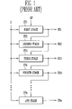
- FIG. 1 is a block diagram showing a conventional scan driving circuit.
- the conventional scan driving circuit includes a plurality of stages ST 1 to STn, which are dependently coupled with a start pulse SP input line.
- the plurality of stages ST 1 to STn sequentially shift a clock signal C in response to a start pulse SP to generate output signals SO 1 to SOn, respectively.
- each of second to n-th stages ST 2 to STn receives and shifts an output signal of a previous stage as a start pulse.
- the stages generate output signals SO 1 to SOn in such a way that the start pulse is sequentially shifted, and provide the output signals to the pixel array.
- FIG. 2 is a circuit diagram of a stage in the scan driving circuit shown in FIG. 1 .
- FIG. 3 is a timing diagram of the stage shown in FIG. 2 .
- each stage of a scan driving circuit uses a master-slave flip-flop. When a clock CLK is at a low level, such a flip-flop continues to receive an input and maintains a previous output.
- the flip-flop maintains an input In received at an input terminal when the clock CLK is at the low level, and outputs the received input, but no longer receives the input In.
- an inverter included in the flip-flop has a problem in that a static current flows when an input thereof is at a low level. Furthermore, in the flip-flop, the number of inverters having received a high-level input is the same number as that of inverters having received a low-level input. Accordingly, the static current flows through a half of all the inverters in the flip-flop, thereby causing power consumption to be increased.
- a voltage value due to a ratio of resistance i.e., transistors M 1 ′ and M 2 ′
- a ratio of resistance i.e., transistors M 1 ′ and M 2 ′
- Low level of the output voltage OUT is set to be greater than that of the ground GND by a threshold voltage of the transistor M 2 ′.
- the deviation in a low level of the output voltage causes a deviation in on-resistance of an input transistor of an inverter included in the circuit of FIG. 2 to occur, thereby weighting a deviation in a high level of the output voltage.
- a panel of an organic light emitting display uses a transistor having a great characteristic deviation, such a problem is more serious.
- an electric current flows through an input transistor to charge an output terminal, whereas the electric current flows through a load transistor to discharge the output terminal.
- a source-gate voltage of the load transistor is gradually reduced, and a discharge current is accordingly reduced rapidly. This causes the discharge efficiency to be deteriorated.
- the scan driving circuit may be implemented with PMOS transistors or NMOS transistors, which switch an output voltage of the scan driving circuit from a positive source voltage to a negative source voltage.
- a scan driving circuit including a plurality of stages.
- the plurality of stages are adapted to receive four clocks.
- Each of the plurality of stages is configured to receive three of the four clocks, to receive and delay an input signal through an input terminal, and to output an output signal through an output terminal.
- the input terminal of each of the plurality of stages is connected to an output terminal of a previous one of the stages.
- Each of the plurality of stages includes a transistor, a switch section, and a storage section. The transistor turns on/off a connection of the input terminal according to a second clock among the clocks, the second clock for inputting through a second clock terminal.
- the switch section transfers a first voltage to the output terminal according to a first clock among the clocks, and prevents the first voltage from being transferred to the output terminal according to the input signal, the first clock for inputting through the first clock terminal.
- the storage section maintains a voltage of the output terminal for a predetermined time, and transfers a voltage of a third clock among the clocks to the output terminal according to the input signal, the third clock for inputting through a third clock terminal.
- a scan driving circuit having a plurality of stages.
- the plurality of stages are adapted to receive four clocks.
- Each of the plurality of stages is configured to receive three of the four clocks, to receive and delay an input signal through an input terminal, and to output an output signal through an output terminal.
- the input terminal of each of the plurality of stages is connected to the output terminal of a previous one of the stages.
- Each of the plurality of stages includes a transistor, a switch section, and a storage section. The transistor turns on/off a connection of the input terminal according to a second clock among the clocks, the second clock for inputting through a second clock terminal.
- the switch section transfers a first voltage to the output terminal according to a first clock among the clocks, the first clock for inputting through the first clock terminal.
- the storage section maintains a voltage of the output terminal for a predetermined time, and transfers a voltage of a third clock among the clocks to the output terminal according to the input signal, the third clock for inputting through a third clock terminal.
- an organic light emitting display having a display region having a plurality of pixels for displaying an image.
- the organic light emitting display also includes a scan driving circuit and a data driving circuit.
- the scan driving circuit is for transferring a scan signal to the display region
- the data driving circuit is for transferring a data signal to the display region.
- the scan driving circuit includes a plurality of stages. The plurality of stages are adapted to receive four clocks. Each of the plurality of stages is configured to receive three of the four clocks, to receive and delay an input signal through an input terminal, and to output an output signal through an output terminal. The input terminal of each of the plurality of stages is connected to the output terminal of a previous one of the stages.
- Each of the plurality of stages includes a transistor, a switch section, and a storage section.
- the transistor turns on/off a connection of the input terminal according to a second clock among the clocks, the second clock for inputting through a second clock terminal.
- the switch section transfers a first voltage to the output terminal according to a first clock among the clocks, and prevents the first voltage from being transferred to the output terminal according to the input signal, the first clock for inputting through a first clock terminal.
- the storage section maintains a voltage of the output terminal for a predetermined time, and transfers a voltage of a third clock among the clocks to the output terminal according to the input signal, the third clock for inputting through a third clock terminal.
- An organic light emitting display having a display region having a plurality of pixels for displaying an image.
- the organic light emitting display also includes a scan driving circuit and a data driving circuit.
- the scan driving circuit is for transferring a scan signal to the display region, and a data driving circuit is for transferring a data signal to the display region.
- the scan driving circuit includes a plurality of stages. The plurality of stages is adapted to receive four clocks. Each of the plurality of stages is configured to receive three of the four s clocks, to receive and delay an input signal through an input terminal, and to output an output signal through an output terminal. The input terminal of each of the plurality of stages is connected to the output terminal of a previous one of the stages.
- Each of the plurality of stages includes a transistor, a switch section, and a storage section.
- the transistor turns on/off a connection of the input terminal according to a second clock among the clocks, the second clock for inputting through a second clock terminal.
- the switch section transfers a first voltage to the output terminal according to a first clock among the clocks, the first clock for inputting through the first clock terminal.
- the storage section maintains a voltage of the output terminal for a predetermined time, and transfers a voltage of a third clock among the clocks to the output terminal according to the input signal, the third clock for inputting through a third clock terminal.
- FIG. 1 is a block diagram showing a conventional scan driving circuit
- FIG. 2 is a circuit diagram of a stage in the scan driving circuit shown in FIG. 1 ;
- FIG. 2A is a circuit diagram of an inverter in the stage shown in FIG. 2 ;
- FIG. 3 is a timing diagram of the stage shown in FIG. 2 ;
- FIG. 4 is a block diagram showing an organic light emitting display according to an embodiment of the present invention.
- FIG. 5 is a block diagram showing a construction of a scan driving circuit according to an embodiment of the present invention.
- FIG. 6 is a circuit diagram showing a first embodiment of a stage of the scan driving circuit shown in FIG. 5 ;
- FIG. 7 is a timing diagram showing a first embodiment of an input/output waveform of the stage shown in FIG. 6 ;
- FIG. 8 is a circuit diagram showing a second embodiment of a stage of the scan driving circuit shown in FIG. 5 ;
- FIG. 9 is a circuit diagram showing a third embodiment of a stage of the scan driving circuit shown in FIG. 5 ;
- FIG. 10 is a circuit diagram showing a fourth embodiment of a stage of the scan driving circuit shown in FIG. 5 ;
- FIG. 11 is a circuit diagram showing a fifth embodiment of a stage of the scan driving circuit shown in FIG. 5 ;
- FIG. 12 is a timing diagram of the stage shown in FIG. 11 ;
- FIG. 13 is a circuit diagram showing a sixth embodiment of a stage of the scan driving circuit shown in FIG. 5 ;
- FIG. 14 is a timing diagram of the stage shown in FIG. 13 .
- first element when a first element is described as being connected to a second element, the first element may be not only directly connected to the second element but also may be indirectly connected to the second element via a third element. Further, elements that are not essential to the complete understanding of the invention are omitted for clarity. Also, like reference numerals refer to like elements throughout.
- FIG. 4 is a block diagram showing an organic light emitting display according to an embodiment of the present invention.
- the organic light emitting display includes a display region 30 , a scan driving circuit 10 , a data driving circuit 20 , and a timing controller 50 .
- the display region 30 includes a plurality of pixels 40 formed at crossing areas of scan lines S 1 to Sn, and data lines D 1 to Dm.
- the scan driving circuit 10 drives the scan lines S 1 to Sn.
- the data driving circuit 20 drives the data lines D 1 to Dm.
- the timing controller 50 controls the scan driving circuit 10 and the data driving circuit 20 .
- the timing controller 50 generates a data drive control signal DCS and a scan drive control signal SCS according to externally supplied synchronous signals.
- the data drive control signal DCS generated by the timing controller 50 is provided to the data driving circuit 20
- the scan drive control signal SCS is provided to the scan driving circuit 10 .
- the timing controller 50 provides externally supplied data Data to the data driving circuit 20 .
- the data driving circuit 20 receives the data drive control signal DCS from the timing controller 50 . Upon the receipt of the data drive control signal DCS, the data driving circuit 20 generates data signals, and provides the generated data signals to the data lines D 1 to Dm. In this embodiment, the data driving circuit 20 provides the generated data signals to the data lines D 1 to Dm every one horizontal period.
- the display region 30 receives a first power from a first power supply ELVDD and a second power from a second power supply ELVSS from an exterior source, and provides them to the pixels 40 .
- the pixels 40 control an amount of current that flows into the second power supply ELVSS from the first power supply ELVDD through a light emitting element corresponding to the data signal, thus generating light corresponding to the data signal.
- the scan driving circuit 10 generates a scan signal in response to a scan drive control signal SCS from the timing controller 50 , and sequentially provides the generated scan signal to the scan lines S 1 to Sn. That is, the scan driving circuit 10 sequentially generates the scan signal to drive the plurality of pixels, and provides the scan signal to the display region 30 .
- FIG. 5 is a block diagram showing a configuration of a scan driving circuit 30 according to an embodiment of the present invention.
- the scan driving circuit includes n stages that are dependently coupled with a start pulse input line so as to drive an m ⁇ n pixel array.
- First output lines of the first n stages are coupled with first n scan lines (i.e., row lines) included in the pixel array.
- a start pulse SP is supplied to a first stage.
- Output signals of first to n ⁇ 1 th stages are provided to next stages as a start pulse, respectively.
- Each stage receives and operates according to a first clock CLK 1 , a second clock CLK 2 , and a third clock CLK 3 ; the second clock CLK 2 , the third clock CLK 3 , and a fourth clock CLK 4 ; the third clock CLK 3 , the fourth clock CLK 4 , and the first clock CLK 1 ; or the fourth clock CLK 4 , the first clock CLK 1 , and the second clock CLK 2 .
- Each stage includes a first clock terminal ck 1 , a second clock terminal ck 2 , and a third clock terminal ck 3 .
- the first clock CLK 1 , the second clock CLK 2 , and the third clock CLK 3 are supplied to the first clock terminal ck 1 , the second clock terminal ck 2 , and the third clock terminal ck 3 of a (4 k-3)-th stage, respectively.
- the second clock CLK 2 , the third clock CLK 3 , and the fourth clock CLK 4 are supplied to the first clock terminal ck 1 , the second clock terminal ck 2 , and the third clock terminal ck 3 of a (4 k-2)-th stage, respectively.
- the first clock CLK 1 , the third clock CLK 3 , and the fourth clock CLK 4 are supplied to the third clock terminal ck 3 , the first clock terminal ck 1 , and the second clock terminal ck 2 of a (4 k-1)-th stage, respectively.
- the first clock CLK 1 , the second clock CLK 2 , and the fourth clock CLK 4 are supplied to the second clock terminal ck 2 , the third clock terminal ck 3 , and the first clock terminal ck 1 of a (4 k)-th stage, respectively.
- k is a natural number.
- each stage operates in response to three of the four supplied clocks: the first clock CLK 1 , the second clock CLK 2 , the third clock CLK 3 , and the fourth clock CLK 4 .
- the second stage receives and operates according to the second clock CLK 2 , the third clock CLK 3 , and the fourth clock CLK 4 .
- the third stage receives and operates according to the third clock CLK 3 , the fourth clock CLK 4 , and the first clock CLK 1 .
- the fourth stage When the third stage outputs a signal in response to the third clock CLK 3 , the fourth clock CLK 4 , and the first clock CLK 1 , the fourth stage receives and operates according to the fourth clock CLK 4 , the first clock CLK 1 , and the second clock CLK 2 . That is, the first, second, third, and fourth stages sequentially output the signal to sequentially drive a display region of an organic light emitting display by lines.
- An external control circuit (not shown) provides the input signals of the driving circuit, that is, a start pulse SP, the first to fourth clocks CLK 1 to CLK 4 , and a supply voltage VDD.
- FIG. 6 is a circuit diagram showing a first embodiment of a stage of the scan driving circuit shown in FIG. 5 .
- FIG. 7 is a timing diagram showing a first embodiment of an input/output waveform of the stage shown in FIG. 6 .
- transistors included in each stage are all PMOS transistors.
- Each stage sequentially sends a low level output through the scan driving circuit.
- the scan driving circuit outputs a high level signal to a display region of an active matrix type display device such as an organic light emitting display for most of the time, and sequentially outputs a low level pulse through a plurality of stages as shown in FIG. 6 and FIG. 7 .
- the stage includes a first PMOS transistor M 1 , a second PMOS transistor M 2 , a third PMOS transistor M 3 , a fourth PMOS transistor M 4 , a fifth PMOS transistor M 5 , and a first capacitor C 1 .
- the first PMOS transistor M 1 includes a gate coupled with a second clock terminal ck 2 , receives an output voltage Si of a previous stage or a first start pulse SP, and selectively transfers the output voltage Si of a previous stage or the first start pulse SP to a first node N 1 .
- the second PMOS transistor M 2 includes a gate connected to the first node N 1 , and is coupled between the third clock terminal ck 3 and a second node N 2 .
- the third PMOS transistor M 3 includes a gate connected to the first clock terminal ck 1 , and is connected between a ground and a third node N 3 .
- the fourth PMOS transistor M 4 includes a gate connected to the first node N 1 , and is connected between the first clock terminal ck 1 and the third node N 3 .
- the fifth PMOS transistor M 5 includes a gate connected to the third node N 3 , and is coupled between a power supply line VDD and the second node N 2 .
- the first capacitor C 1 is connected between the first node N 1 and the second node N 2 , and maintains a predetermined voltage.
- M 3 is coupled to a ground
- M 3 may alternatively be coupled to a negative power supply VSS.
- each stage of the scan driving circuit may divide one period into a precharge period, an input period, an evaluation period, and a quiescent period according to the first clock CLK 1 , the second clock CLK 2 , the third clock CLK 3 , and the fourth clock CLK 4 .
- a precharge period a low level signal is inputted to the first clock terminal ck 1 of the stage, and a high level signal is inputted to the second clock terminal ck 2 and the third clock terminal ck 3 to precharge a capacitor C 1 of the stage.
- a low level signal is inputted to the second clock terminal ck 2 , and a high level signal is inputted to the first clock terminal ck 1 and the third clock terminal ck 3 .
- a start pulse SP or a scan signal Si of a previous stage is inputted through the input terminal to the first node N 1 and is stored in the capacitor C 1 .
- a low level signal is inputted to the third clock terminal ck 3 , and a high level signal is inputted to the first clock terminal ck 1 and the second clock terminal ck 2 , so that the stage outputs a low level signal within a predetermined period.
- a start pulse SP or a scan signal Si of a previous stage is inputted through the input terminal.
- the quiescent period is a time period when the fourth clock CLK 4 which was not inputted to the stage has a low level.
- the third PMOS transistor M 3 is turned-on to make a voltage of the third node N 3 a ground voltage. Accordingly, the fifth PMOS transistor M 5 is turned-on to output a voltage of a power supply voltage VDD through an output terminal out, with the result that a high level voltage is outputted to the output terminal out. That is, a scan signal is outputted with a high level.
- the second clock CLK 2 becomes a low level, the start pulse SP or the scan signal Si of a previous stage is transferred to the first node N 1 through the first PMOS transistor M 1 , and the start pulse SP or the scan signal Si of a previous stage is stored in the capacitor C 1 .
- the second PMOS transistor M 2 and the fourth PMOS transistor M 4 are turned-on. Further, the first clock CLK 1 becomes a high level to turn-off the third PMOS transistor M 3 .
- a first clock CLK 1 of a high level is transferred to the third node N 3 to turn-off the fifth PMOS transistor M 5 .
- the second PMOS transistor M 2 is turned-off, so that an output terminal outputs a high level signal according to a third clock CLK 3 of a high level.
- the third clock CLK 3 becomes a low level to float the first PMOS transistor M 1 .
- This causes the capacitor C 1 to maintain a low level signal, thereby turning-on the second PMOS transistor M 2 and the fourth PMOS transistor M 4 .
- the third PMOS transistor M 3 and the fifth PMOS transistor M 5 are turned-off. Consequently, a low level signal is outputted to the output terminal out according to the third clock CLK 3 of a low level.
- the output terminal out outputs a high level voltage by a power supply line VDD during the precharge period, and maintains a high level voltage by the capacitor C 1 during the input period. Further, during the evaluation period, a voltage corresponding to the third clock CLK 3 of a low level is outputted. When the third clock CLK 3 becomes a low level, a voltage of the output terminal out drops. In contrast to this, when the third clock CLK 3 becomes a high level, the voltage of the output terminal out again becomes a high level. Accordingly, the output terminal out outputs a scan signal.
- the first clock CLK 1 , the second clock CLK 2 , and the third clock CLK 3 are transferred with a high level, but the fourth clock CLK 4 of a low level is not transferred to the stage, so that the stage does not operate in response to clocks.
- the second PMOS transistor M 2 is turned-off, so that the output terminal out maintains a high level signal.
- each stage receives the start pulse SP or a low level signal of a previous stage, it outputs a low level signal that results in a sequential output of the scan signal.
- FIG. 8 is a circuit diagram showing a second embodiment of a stage of the scan driving circuit shown in FIG. 5 .
- the second embodiment of a stage includes a first PMOS transistor M 1 , a second PMOS transistor M 2 , a third PMOS transistor M 3 , a fourth PMOS transistor M 4 , a fifth PMOS transistor M 5 , and a capacitor C 1 .
- the first PMOS transistor M 1 transfers an input signal to the first node N 1 in response to the second clock CLK 2
- the second PMOS transistor M 2 transfers the third clock CLK 3 to the second node N 2 corresponding to a voltage of the first node N 1
- the third PMOS transistor M 3 transfers a ground voltage to a gate of the fifth transistor PMOS M 5 in response to the first clock CLK 1
- a gate of the fourth PMOS transistor M 4 is connected to the output terminal out, and the fourth transistor M 4 transfers the first clock CLK 1 to a gate of the fifth PMOS transistor M 5 corresponding to a voltage of the output terminal out.
- the fifth PMOS transistor M 5 transfers a voltage of a power supply line VDD to the output terminal corresponding to a voltage of a gate thereof.
- the capacitor C 1 is connected between the first node N 1 and the second node N 2 , and maintains a predetermined voltage.
- the stage having the construction as described above receives and operates according to the first to third clocks CLK 1 to CLK 3 shown in FIG. 7 .
- the fifth PMOS transistor M 5 is turned-on in response to the first clock CLK 1 to output a high level signal to the output terminal out by a voltage of the power supply line VDD.
- the start pulse SP or a scan signal Si of a previous stage is stored in the capacitor C 1 in response to the second clock CLK 2 .
- the voltage stored in the capacitor C 1 causes a voltage of the third clock CLK 3 to be outputted, so that the output terminal out maintains a high level signal.
- the fourth PMOS transistor M 4 transfers a high level signal to a gate of the fifth PMOS transistor M 5 , thereby preventing a voltage of the power supply line VDD from being transferred to the output terminal.
- FIG. 9 is a circuit diagram showing a third embodiment of a stage of the scan driving circuit shown in FIG. 5 .
- the stage shown in FIG. 9 has substantially the same construction and functions as those of FIG. 6 .
- the difference of the stage of FIG. 9 from that of the FIG. 6 is that the sixth PMOS transistor M 6 is connected to a source of the fourth PMOS transistor M 6 , and a power supply line VDD is connected to a source of the sixth PMOS transistor M 6 . Accordingly, when the third clock CLK 3 has a low level, the fourth PMOS transistor M 4 is turned-on, so that a voltage of the power supply line VDD is transferred to the third node N 3 to turn-off the fifth PMOS transistor M 5 .
- the voltage of the power supply line VDD which is not a clock is transferred to a gate of the fifth PMOS transistor M 5 to ensure a turning-off state of the fifth PMOS transistor M 5 . Accordingly, when the third clock CLK 3 has a low level, the stage prevents a voltage of the power supply line VDD from being transferred to an output terminal through the fifth PMOS transistor M 5 . Thus, when the third clock CLK 3 has a low level, the stage ensures a voltage of the output terminal to be dropped to a low level.
- FIG. 10 is a circuit diagram showing a fourth embodiment of a stage of the scan driving circuit shown in FIG. 5 .
- a stage of FIG. 10 has substantially the same construction and functions as those of FIG. 9 .
- the third clock CLK 3 has a low level
- a voltage of the power supply line VDD is transferred to the third node N 3 in the same manner as that of FIG. 9 .
- the difference of a stage of FIG. 10 from that of the FIG. 9 is that the third clock CLK 3 is transferred to a gate of the fourth PMOS transistor M 4 , and a gate of the sixth PMOS transistor M 6 is connected to the third node N 3 .
- FIG. 11 is a circuit diagram showing a fifth embodiment of a stage of the scan driving circuit shown in FIG. 5 .
- a stage of FIG. 11 has substantially the same construction and functions as those of FIG. 8 except that a source and a gate of a third PMOS transistor M 3 receive the first clock CLK 1 . Accordingly, when the first clock CLK 1 has a low level, the fifth PMOS transistor M 5 is turned-on. Remaining operations of the stage shown in the FIG. 11 is the same as that of FIG. 8 .
- FIG. 12 is a timing diagram of the stage shown in FIG. 11 .
- signal waveforms of FIG. 12 are applicable to stages of FIG. 8 to FIG. 11 .
- FIG. 11 shows an operation of the stage when at least two of the first to fourth clocks CLK 1 to CLK 4 overlap with each other by external influences.
- the scan signal operates corresponding to an operation of the third clock CLK 3 .
- the fourth clock CLK 4 is not inputted to the stage, so that the fourth clock CLK 4 does not influence an operation of the stage. Accordingly, an output scan signal of the stage varies depending on a waveform of the third clock CLK 3 . As a result, even if certain parts of respective clocks overlap with each other, a waveform of the scan signal is not distorted.
- FIG. 13 is a circuit diagram showing a sixth embodiment of a stage of the scan driving circuit shown in FIG. 5 .
- FIG. 14 is a timing diagram of the stage shown in FIG. 13 .
- the stage is constructed by NMOS transistors M 6 , M 7 , M 8 , M 9 , and M 10 .
- a stage of FIG. 13 has substantially the same construction as that of FIG. 6 , and respective transistors perform substantially the same operation as that of FIG. 6 .
- the transistors M 6 , M 7 , M 8 , M 9 , and M 10 perform substantially the same functions as transistors M 1 , M 2 , M 3 , M 4 , and M 5 , respectively.
- the scan driving circuit and an organic light emitting display using the same of exemplary embodiments according to the present invention switch an output voltage from a positive source voltage to a negative source voltage, an operation speed is increased. Furthermore, even if a clock transferred to the scan driving circuit is erroneously operated, a change of a waveform of a scan signal is not great.
Landscapes
- Engineering & Computer Science (AREA)
- Physics & Mathematics (AREA)
- Computer Hardware Design (AREA)
- General Physics & Mathematics (AREA)
- Theoretical Computer Science (AREA)
- Microelectronics & Electronic Packaging (AREA)
- Power Engineering (AREA)
- Control Of Indicators Other Than Cathode Ray Tubes (AREA)
- Control Of El Displays (AREA)
- Electroluminescent Light Sources (AREA)
- Shift Register Type Memory (AREA)
Abstract
Description
Claims (24)
Applications Claiming Priority (2)
| Application Number | Priority Date | Filing Date | Title |
|---|---|---|---|
| KR10-2006-0034960 | 2006-04-18 | ||
| KR1020060034960A KR100776511B1 (en) | 2006-04-18 | 2006-04-18 | Scan driving circuit and organic light emitting display device using same |
Publications (2)
| Publication Number | Publication Date |
|---|---|
| US20070242000A1 US20070242000A1 (en) | 2007-10-18 |
| US7679597B2 true US7679597B2 (en) | 2010-03-16 |
Family
ID=38157787
Family Applications (1)
| Application Number | Title | Priority Date | Filing Date |
|---|---|---|---|
| US11/657,669 Active 2028-10-18 US7679597B2 (en) | 2006-04-18 | 2007-01-23 | Scan driving circuit and organic light emitting display using the same |
Country Status (5)
| Country | Link |
|---|---|
| US (1) | US7679597B2 (en) |
| EP (1) | EP1847983B1 (en) |
| JP (1) | JP2007286583A (en) |
| KR (1) | KR100776511B1 (en) |
| CN (1) | CN100565642C (en) |
Cited By (5)
| Publication number | Priority date | Publication date | Assignee | Title |
|---|---|---|---|---|
| US20070242001A1 (en) * | 2006-04-18 | 2007-10-18 | Dong Yong Shin | Scan driving circuit and organic light emitting display using the same |
| US20120294411A1 (en) * | 2011-05-19 | 2012-11-22 | Boe Technology Group Co., Ltd. | Shift register and row-scan driving circuit |
| US20140079175A1 (en) * | 2012-05-21 | 2014-03-20 | Boe Technology Group Co., Ltd. | Shift Register Driving Apparatus And Display |
| CN107731151A (en) * | 2017-11-30 | 2018-02-23 | 信利(惠州)智能显示有限公司 | Array base palte and display device |
| US9905192B2 (en) | 2015-01-20 | 2018-02-27 | Boe Technology Group Co., Ltd. | GOA unit and driving method, GOA circuit and display device |
Families Citing this family (21)
| Publication number | Priority date | Publication date | Assignee | Title |
|---|---|---|---|---|
| KR100924143B1 (en) | 2008-04-02 | 2009-10-28 | 삼성모바일디스플레이주식회사 | Flat Panel Display and Driving Method |
| KR100986862B1 (en) * | 2009-01-29 | 2010-10-08 | 삼성모바일디스플레이주식회사 | Light emission control line driver and organic light emitting display device using the same |
| US8957843B2 (en) | 2010-02-25 | 2015-02-17 | Samsung Display Co., Ltd. | Gate selection circuit of liquid crystal panel, accumulating capacity driving circuit, driving device, and driving method |
| KR101108172B1 (en) | 2010-03-16 | 2012-01-31 | 삼성모바일디스플레이주식회사 | Scan Driver and Organic Light Emitting Display Using the Same |
| KR101944465B1 (en) * | 2011-01-06 | 2019-02-07 | 삼성디스플레이 주식회사 | Emission Driver and Organic Light Emitting Display Device Using the same |
| KR101891651B1 (en) * | 2011-11-14 | 2018-08-27 | 삼성디스플레이 주식회사 | Scan driving device and driving method thereof |
| KR20130055253A (en) * | 2011-11-18 | 2013-05-28 | 삼성디스플레이 주식회사 | Scan driving device and driving method thereof |
| KR101911872B1 (en) * | 2011-11-18 | 2018-10-26 | 삼성디스플레이 주식회사 | Scan driving device and driving method thereof |
| KR101878374B1 (en) * | 2012-04-26 | 2018-07-16 | 삼성디스플레이 주식회사 | Scan driving device and driving method thereof |
| KR101879779B1 (en) * | 2012-06-01 | 2018-07-19 | 삼성디스플레이 주식회사 | Display device, inspecting and driving method thereof |
| KR101975864B1 (en) * | 2012-10-25 | 2019-05-08 | 삼성디스플레이 주식회사 | Scan driving device and repair method thereof |
| CN103268749B (en) * | 2012-11-21 | 2015-04-15 | 上海天马微电子有限公司 | Inverter, AMOLED compensation circuit and display panel |
| TWI520117B (en) * | 2014-02-07 | 2016-02-01 | 友達光電股份有限公司 | Shift control cell |
| CN104700769B (en) * | 2015-04-09 | 2017-03-15 | 京东方科技集团股份有限公司 | Shift register cell, gate drive apparatus and display device |
| US20160365042A1 (en) * | 2015-06-15 | 2016-12-15 | Apple Inc. | Display Driver Circuitry With Gate Line and Data Line Delay Compensation |
| CN106057131B (en) * | 2016-05-27 | 2018-11-23 | 武汉华星光电技术有限公司 | Scan drive circuit and flat display apparatus with the circuit |
| CN110164347B (en) * | 2018-05-08 | 2020-11-13 | 京东方科技集团股份有限公司 | Shift register unit and driving method thereof, scanning driving circuit and display device |
| CN110164360B (en) * | 2018-06-14 | 2022-02-11 | 友达光电股份有限公司 | Gate driving device |
| CN110164381B (en) * | 2018-06-14 | 2022-01-21 | 友达光电股份有限公司 | Gate driving device |
| CN110010079B (en) * | 2018-06-14 | 2020-10-23 | 友达光电股份有限公司 | gate drive |
| CN111243513B (en) * | 2020-03-13 | 2021-07-20 | Oppo广东移动通信有限公司 | A control circuit and control method |
Citations (11)
| Publication number | Priority date | Publication date | Assignee | Title |
|---|---|---|---|---|
| JP2000155550A (en) | 1998-10-21 | 2000-06-06 | Lg Philips Lcd Co Ltd | Shift register |
| JP2001160299A (en) | 1999-12-02 | 2001-06-12 | Casio Comput Co Ltd | Shift register and electronic device |
| US6426743B1 (en) * | 1999-02-09 | 2002-07-30 | Lg. Philips Lcd Co., Ltd | Shift register |
| KR20020085205A (en) | 2001-05-07 | 2002-11-16 | 엘지.필립스 엘시디 주식회사 | Shift Resistor Circuit |
| JP2003101394A (en) | 2001-05-29 | 2003-04-04 | Semiconductor Energy Lab Co Ltd | Pulse output circuit, shift register and display unit |
| US20030128180A1 (en) * | 2001-12-12 | 2003-07-10 | Kim Byeong Koo | Shift register with a built in level shifter |
| JP2004185684A (en) | 2002-11-29 | 2004-07-02 | Toshiba Matsushita Display Technology Co Ltd | Bidirectional shift register, drive circuit using the same, flat-panel display device |
| US20040227718A1 (en) | 2003-05-12 | 2004-11-18 | Lg.Philips Lcd Co., Ltd. | Shift register |
| JP2005166139A (en) | 2003-12-01 | 2005-06-23 | Seiko Epson Corp | Shift register, driving method thereof, driving circuit, electro-optical device, and electronic apparatus |
| JP2005251335A (en) | 2004-03-05 | 2005-09-15 | Casio Comput Co Ltd | Shift register circuit, drive control method thereof, and drive control apparatus |
| US7420536B2 (en) * | 2003-12-30 | 2008-09-02 | Lg Display Co., Ltd. | Active matrix display device |
Family Cites Families (1)
| Publication number | Priority date | Publication date | Assignee | Title |
|---|---|---|---|---|
| KR101055208B1 (en) * | 2004-11-11 | 2011-08-08 | 엘지디스플레이 주식회사 | Shift register |
-
2006
- 2006-04-18 KR KR1020060034960A patent/KR100776511B1/en not_active Expired - Lifetime
- 2006-10-25 JP JP2006289875A patent/JP2007286583A/en active Pending
-
2007
- 2007-01-23 US US11/657,669 patent/US7679597B2/en active Active
- 2007-04-03 EP EP07251479A patent/EP1847983B1/en not_active Ceased
- 2007-04-10 CN CNB2007100971725A patent/CN100565642C/en not_active Expired - Fee Related
Patent Citations (11)
| Publication number | Priority date | Publication date | Assignee | Title |
|---|---|---|---|---|
| JP2000155550A (en) | 1998-10-21 | 2000-06-06 | Lg Philips Lcd Co Ltd | Shift register |
| US6426743B1 (en) * | 1999-02-09 | 2002-07-30 | Lg. Philips Lcd Co., Ltd | Shift register |
| JP2001160299A (en) | 1999-12-02 | 2001-06-12 | Casio Comput Co Ltd | Shift register and electronic device |
| KR20020085205A (en) | 2001-05-07 | 2002-11-16 | 엘지.필립스 엘시디 주식회사 | Shift Resistor Circuit |
| JP2003101394A (en) | 2001-05-29 | 2003-04-04 | Semiconductor Energy Lab Co Ltd | Pulse output circuit, shift register and display unit |
| US20030128180A1 (en) * | 2001-12-12 | 2003-07-10 | Kim Byeong Koo | Shift register with a built in level shifter |
| JP2004185684A (en) | 2002-11-29 | 2004-07-02 | Toshiba Matsushita Display Technology Co Ltd | Bidirectional shift register, drive circuit using the same, flat-panel display device |
| US20040227718A1 (en) | 2003-05-12 | 2004-11-18 | Lg.Philips Lcd Co., Ltd. | Shift register |
| JP2005166139A (en) | 2003-12-01 | 2005-06-23 | Seiko Epson Corp | Shift register, driving method thereof, driving circuit, electro-optical device, and electronic apparatus |
| US7420536B2 (en) * | 2003-12-30 | 2008-09-02 | Lg Display Co., Ltd. | Active matrix display device |
| JP2005251335A (en) | 2004-03-05 | 2005-09-15 | Casio Comput Co Ltd | Shift register circuit, drive control method thereof, and drive control apparatus |
Non-Patent Citations (9)
| Title |
|---|
| English abstract for GB 2343068, dated Apr. 6, 2000, corresponding to JP 2000-155550 listed above. |
| European Search Report dated Jul. 2, 2007, for 07251479.7, in the name of Samsung SDI Co, Ltd. |
| Japan Patent Abstracts, Publication No. 2005-251335, dated Sep. 15, 2005, in the name of Katsuhiko Morosawa. |
| Korean Patent Abstracts, Publication No. 1020020085205 A, dated Nov. 16, 2002, in the name of Han Sang Lee et al. |
| Patent Abstracts of Japan, Publication No. 2000-155550, dated Jun. 6, 2000, in the name of Ju Cheon Yeo et al. |
| Patent Abstracts of Japan, Publication No. 2001-160299, dated Jun. 12, 2001, in the name of Katsuhiko Morosawa et al. |
| Patent Abstracts of Japan, Publication No. 2003-101394, dated Apr. 4, 2003, in the name of Sho Nagao et al. |
| Patent Abstracts of Japan, Publication No. 2004-185684; Publication Date: Jul. 2, 2004; in the name of Kitani et al. |
| Patent Abstracts of Japan, Publication No. 2005-166139; Publication Date: Jun. 23, 2005; in the name of Ozawa et al. |
Cited By (7)
| Publication number | Priority date | Publication date | Assignee | Title |
|---|---|---|---|---|
| US20070242001A1 (en) * | 2006-04-18 | 2007-10-18 | Dong Yong Shin | Scan driving circuit and organic light emitting display using the same |
| US7920118B2 (en) * | 2006-04-18 | 2011-04-05 | Samsung Mobile Display Co., Ltd. | Scan driving circuit comprising a plurality of stages, each stage configured to receive multiple clocks |
| US20120294411A1 (en) * | 2011-05-19 | 2012-11-22 | Boe Technology Group Co., Ltd. | Shift register and row-scan driving circuit |
| US8885792B2 (en) * | 2011-05-19 | 2014-11-11 | Boe Technology Group Co., Ltd. | Shift register and row-scan driving circuit |
| US20140079175A1 (en) * | 2012-05-21 | 2014-03-20 | Boe Technology Group Co., Ltd. | Shift Register Driving Apparatus And Display |
| US9905192B2 (en) | 2015-01-20 | 2018-02-27 | Boe Technology Group Co., Ltd. | GOA unit and driving method, GOA circuit and display device |
| CN107731151A (en) * | 2017-11-30 | 2018-02-23 | 信利(惠州)智能显示有限公司 | Array base palte and display device |
Also Published As
| Publication number | Publication date |
|---|---|
| KR100776511B1 (en) | 2007-11-16 |
| US20070242000A1 (en) | 2007-10-18 |
| KR20070103183A (en) | 2007-10-23 |
| EP1847983B1 (en) | 2012-01-25 |
| JP2007286583A (en) | 2007-11-01 |
| CN101059933A (en) | 2007-10-24 |
| EP1847983A1 (en) | 2007-10-24 |
| CN100565642C (en) | 2009-12-02 |
Similar Documents
| Publication | Publication Date | Title |
|---|---|---|
| US7679597B2 (en) | Scan driving circuit and organic light emitting display using the same | |
| US8232954B2 (en) | Shift register and organic light emitting display device using the same | |
| US8284150B2 (en) | Shift register and organic light emitting display device using the same | |
| KR100658269B1 (en) | Scan Driving Circuit and Organic Electroluminescent Device Using the Same | |
| KR101756667B1 (en) | Shift register and display device including the same | |
| EP1764774B1 (en) | Scan driving circuit and organic light emitting display using the same | |
| KR100805538B1 (en) | Shift register and organic light emitting display device using the same | |
| KR102721846B1 (en) | Emission driver for display device and disaplay device applying thereof | |
| US11263988B2 (en) | Gate driving circuit and display device using the same | |
| KR100762690B1 (en) | Data driving circuit and organic light emitting display device using the same | |
| US8836631B2 (en) | Scan driving circuit with a shift register and electroluminescent display using the same | |
| US7639217B2 (en) | Scan driving circuit and organic light emitting display device using the same | |
| KR100658284B1 (en) | Scan Driving Circuit and Organic Electroluminescent Device Using the Same | |
| US7920118B2 (en) | Scan driving circuit comprising a plurality of stages, each stage configured to receive multiple clocks | |
| KR100759686B1 (en) | Shift register circuit | |
| CN109671382B (en) | Gate drive circuit and display device using the gate drive circuit | |
| KR20110032838A (en) | Shift register | |
| KR100658270B1 (en) | Scan Driving Circuit and Organic Electroluminescent Device Using the Same | |
| KR100662983B1 (en) | Scan Driving Circuit and Organic Electroluminescent Device Using the Same | |
| CN121311934A (en) | Shift registers and their driving methods, scan driving circuits, and display devices |
Legal Events
| Date | Code | Title | Description |
|---|---|---|---|
| AS | Assignment |
Owner name: SAMSUNG SDI CO., LTD., KOREA, REPUBLIC OF Free format text: ASSIGNMENT OF ASSIGNORS INTEREST;ASSIGNOR:SHIN, DONG YONG;REEL/FRAME:019288/0526 Effective date: 20070115 Owner name: SAMSUNG SDI CO., LTD.,KOREA, REPUBLIC OF Free format text: ASSIGNMENT OF ASSIGNORS INTEREST;ASSIGNOR:SHIN, DONG YONG;REEL/FRAME:019288/0526 Effective date: 20070115 |
|
| AS | Assignment |
Owner name: SAMSUNG MOBILE DISPLAY CO., LTD., KOREA, REPUBLIC Free format text: ASSIGNMENT OF ASSIGNORS INTEREST;ASSIGNOR:SAMSUNG SDI CO., LTD.;REEL/FRAME:022079/0517 Effective date: 20081210 Owner name: SAMSUNG MOBILE DISPLAY CO., LTD.,KOREA, REPUBLIC O Free format text: ASSIGNMENT OF ASSIGNORS INTEREST;ASSIGNOR:SAMSUNG SDI CO., LTD.;REEL/FRAME:022079/0517 Effective date: 20081210 |
|
| FEPP | Fee payment procedure |
Free format text: PAYOR NUMBER ASSIGNED (ORIGINAL EVENT CODE: ASPN); ENTITY STATUS OF PATENT OWNER: LARGE ENTITY |
|
| STCF | Information on status: patent grant |
Free format text: PATENTED CASE |
|
| AS | Assignment |
Owner name: SAMSUNG DISPLAY CO., LTD., KOREA, REPUBLIC OF Free format text: MERGER;ASSIGNOR:SAMSUNG MOBILE DISPLAY CO., LTD.;REEL/FRAME:028884/0128 Effective date: 20120702 |
|
| FEPP | Fee payment procedure |
Free format text: PAYER NUMBER DE-ASSIGNED (ORIGINAL EVENT CODE: RMPN); ENTITY STATUS OF PATENT OWNER: LARGE ENTITY Free format text: PAYOR NUMBER ASSIGNED (ORIGINAL EVENT CODE: ASPN); ENTITY STATUS OF PATENT OWNER: LARGE ENTITY |
|
| FPAY | Fee payment |
Year of fee payment: 4 |
|
| MAFP | Maintenance fee payment |
Free format text: PAYMENT OF MAINTENANCE FEE, 8TH YEAR, LARGE ENTITY (ORIGINAL EVENT CODE: M1552) Year of fee payment: 8 |
|
| MAFP | Maintenance fee payment |
Free format text: PAYMENT OF MAINTENANCE FEE, 12TH YEAR, LARGE ENTITY (ORIGINAL EVENT CODE: M1553); ENTITY STATUS OF PATENT OWNER: LARGE ENTITY Year of fee payment: 12 |