US7582976B2 - Semiconductor device tape carrier, manufacturing method for semiconductor device, semiconductor device, and semiconductor module device - Google Patents
Semiconductor device tape carrier, manufacturing method for semiconductor device, semiconductor device, and semiconductor module device Download PDFInfo
- Publication number
- US7582976B2 US7582976B2 US11/896,827 US89682707A US7582976B2 US 7582976 B2 US7582976 B2 US 7582976B2 US 89682707 A US89682707 A US 89682707A US 7582976 B2 US7582976 B2 US 7582976B2
- Authority
- US
- United States
- Prior art keywords
- semiconductor device
- tape
- pitch
- insulative
- semiconductor
- Prior art date
- Legal status (The legal status is an assumption and is not a legal conclusion. Google has not performed a legal analysis and makes no representation as to the accuracy of the status listed.)
- Active
Links
Images


Classifications
-
- H—ELECTRICITY
- H10—SEMICONDUCTOR DEVICES; ELECTRIC SOLID-STATE DEVICES NOT OTHERWISE PROVIDED FOR
- H10W—GENERIC PACKAGES, INTERCONNECTIONS, CONNECTORS OR OTHER CONSTRUCTIONAL DETAILS OF DEVICES COVERED BY CLASS H10
- H10W70/00—Package substrates; Interposers; Redistribution layers [RDL]
- H10W70/60—Insulating or insulated package substrates; Interposers; Redistribution layers
- H10W70/67—Insulating or insulated package substrates; Interposers; Redistribution layers characterised by their insulating layers or insulating parts
- H10W70/688—Flexible insulating substrates
-
- H—ELECTRICITY
- H10—SEMICONDUCTOR DEVICES; ELECTRIC SOLID-STATE DEVICES NOT OTHERWISE PROVIDED FOR
- H10W—GENERIC PACKAGES, INTERCONNECTIONS, CONNECTORS OR OTHER CONSTRUCTIONAL DETAILS OF DEVICES COVERED BY CLASS H10
- H10W70/00—Package substrates; Interposers; Redistribution layers [RDL]
- H10W70/01—Manufacture or treatment
- H10W70/04—Manufacture or treatment of leadframes
-
- H—ELECTRICITY
- H10—SEMICONDUCTOR DEVICES; ELECTRIC SOLID-STATE DEVICES NOT OTHERWISE PROVIDED FOR
- H10W—GENERIC PACKAGES, INTERCONNECTIONS, CONNECTORS OR OTHER CONSTRUCTIONAL DETAILS OF DEVICES COVERED BY CLASS H10
- H10W70/00—Package substrates; Interposers; Redistribution layers [RDL]
- H10W70/40—Leadframes
- H10W70/453—Leadframes comprising flexible metallic tapes
-
- H—ELECTRICITY
- H10—SEMICONDUCTOR DEVICES; ELECTRIC SOLID-STATE DEVICES NOT OTHERWISE PROVIDED FOR
- H10W—GENERIC PACKAGES, INTERCONNECTIONS, CONNECTORS OR OTHER CONSTRUCTIONAL DETAILS OF DEVICES COVERED BY CLASS H10
- H10W74/00—Encapsulations, e.g. protective coatings
- H10W74/01—Manufacture or treatment
- H10W74/012—Manufacture or treatment of encapsulations on active surfaces of flip-chip devices, e.g. forming underfills
-
- H—ELECTRICITY
- H10—SEMICONDUCTOR DEVICES; ELECTRIC SOLID-STATE DEVICES NOT OTHERWISE PROVIDED FOR
- H10W—GENERIC PACKAGES, INTERCONNECTIONS, CONNECTORS OR OTHER CONSTRUCTIONAL DETAILS OF DEVICES COVERED BY CLASS H10
- H10W74/00—Encapsulations, e.g. protective coatings
- H10W74/10—Encapsulations, e.g. protective coatings characterised by their shape or disposition
- H10W74/131—Encapsulations, e.g. protective coatings characterised by their shape or disposition the semiconductor body being only partially enclosed
- H10W74/141—Encapsulations, e.g. protective coatings characterised by their shape or disposition the semiconductor body being only partially enclosed the encapsulations being on at least the sidewalls of the semiconductor body
-
- H—ELECTRICITY
- H10—SEMICONDUCTOR DEVICES; ELECTRIC SOLID-STATE DEVICES NOT OTHERWISE PROVIDED FOR
- H10W—GENERIC PACKAGES, INTERCONNECTIONS, CONNECTORS OR OTHER CONSTRUCTIONAL DETAILS OF DEVICES COVERED BY CLASS H10
- H10W74/00—Encapsulations, e.g. protective coatings
- H10W74/10—Encapsulations, e.g. protective coatings characterised by their shape or disposition
- H10W74/15—Encapsulations, e.g. protective coatings characterised by their shape or disposition on active surfaces of flip-chip devices, e.g. underfills
-
- H—ELECTRICITY
- H05—ELECTRIC TECHNIQUES NOT OTHERWISE PROVIDED FOR
- H05K—PRINTED CIRCUITS; CASINGS OR CONSTRUCTIONAL DETAILS OF ELECTRIC APPARATUS; MANUFACTURE OF ASSEMBLAGES OF ELECTRICAL COMPONENTS
- H05K3/00—Apparatus or processes for manufacturing printed circuits
- H05K3/0097—Processing two or more printed circuits simultaneously, e.g. made from a common substrate, or temporarily stacked circuit boards
-
- H—ELECTRICITY
- H10—SEMICONDUCTOR DEVICES; ELECTRIC SOLID-STATE DEVICES NOT OTHERWISE PROVIDED FOR
- H10W—GENERIC PACKAGES, INTERCONNECTIONS, CONNECTORS OR OTHER CONSTRUCTIONAL DETAILS OF DEVICES COVERED BY CLASS H10
- H10W72/00—Interconnections or connectors in packages
- H10W72/851—Dispositions of multiple connectors or interconnections
- H10W72/853—On the same surface
- H10W72/856—Bump connectors and die-attach connectors
-
- H—ELECTRICITY
- H10—SEMICONDUCTOR DEVICES; ELECTRIC SOLID-STATE DEVICES NOT OTHERWISE PROVIDED FOR
- H10W—GENERIC PACKAGES, INTERCONNECTIONS, CONNECTORS OR OTHER CONSTRUCTIONAL DETAILS OF DEVICES COVERED BY CLASS H10
- H10W90/00—Package configurations
- H10W90/701—Package configurations characterised by the relative positions of pads or connectors relative to package parts
- H10W90/721—Package configurations characterised by the relative positions of pads or connectors relative to package parts of bump connectors
- H10W90/724—Package configurations characterised by the relative positions of pads or connectors relative to package parts of bump connectors between a chip and a stacked insulating package substrate, interposer or RDL
-
- H—ELECTRICITY
- H10—SEMICONDUCTOR DEVICES; ELECTRIC SOLID-STATE DEVICES NOT OTHERWISE PROVIDED FOR
- H10W—GENERIC PACKAGES, INTERCONNECTIONS, CONNECTORS OR OTHER CONSTRUCTIONAL DETAILS OF DEVICES COVERED BY CLASS H10
- H10W90/00—Package configurations
- H10W90/701—Package configurations characterised by the relative positions of pads or connectors relative to package parts
- H10W90/731—Package configurations characterised by the relative positions of pads or connectors relative to package parts of die-attach connectors
- H10W90/734—Package configurations characterised by the relative positions of pads or connectors relative to package parts of die-attach connectors between a chip and a stacked insulating package substrate, interposer or RDL
Definitions
- the present invention relates to a tape carrier used for a semiconductor device composed of semiconductor elements adhered/mounted on a flexible wiring substrate; semiconductor device; semiconductor module; and a manufacturing method for semiconductor device.
- the present invention relates to a tape carrier used for a semiconductor device composed of semiconductor elements bonded/mounted onto a flexible wiring substrate called COF (Chip On Film) or TCP (Tape carrier Package)(these semiconductor devices will be referred to simply as COF and TCP, hereinafter); semiconductor device; semiconductor module; and a manufacturing method for semiconductor device.
- COF Chip On Film
- TCP Transmission carrier Package
- FIG. 15 is a plan view showing a conventional tape carrier 500 for COF semiconductor device (before mounting semiconductor element).
- FIG. 16 is a plan view showing a conventional COF semiconductor device.
- FIG. 17 is a plan view showing a conventional tape carrier 600 for TCP semiconductor device (before mounting semiconductor element).
- FIG. 18 is a plan view showing a conventional TCP semiconductor device.
- a TCP includes an insulative tape 501 with an opening section 516 in a portion where a semiconductor element 521 is mounted, and the tips of the wire patterns 511 projected like cantilevers are bonded with a semiconductor element 521 .
- a COF does not include an element-mounting opening section for mounting the semiconductor element 521 , and the semiconductor element 521 is bonded/mounted onto the wire patterns 511 formed on the surface of the insulative tape 501 of a thin film.
- each wire pattern 511 of the TCP is projected like cantilevers, the thickness of each wire pattern 511 is set to 18 ⁇ m or greater, and therefore it is difficult to produce a wire patterns 511 with a wiring pitch smaller than 45 ⁇ m.
- the COF uses wire patterns 511 formed on the surface of the insulative tape 501 which is a thin film, and it is possible to form wire patterns 511 with a thickness of equal to or less than 8 ⁇ m and a wiring pitch equal to or less than 35 ⁇ m.
- a slit 517 is formed in advance in a folding part to be folded after the device is mounted to a liquid crystal panel or the like. Meanwhile, the COF does not have a slit to be folded, and can be folded at anywhere on the insulative tape 501 of a thin film.
- the TCP has an insulative tape 501 made of polyimide on which a copper foil is laminated through an adhesive. Meanwhile, in the COF, polyimide or the like is applied on the rear surface of a copper foil and then the application layer is cured (casting technology), or by laminating copper on an insulative tape 501 of polyimide or the like by sputtering (metalization technology).
- the COF includes an insulative tape 501 of a thin film which can be freely folded, and each wire of the wire patterns 511 formed on the insulative tape 501 of thin film is conducted to a corresponding terminal of the semiconductor element 521 .
- An external connection section 512 is conducted to a liquid crystal panel, a printed circuit-board or the like.
- the rest of wire pattern exposing section is coated with a solder resist 513 to have an insulative property.
- the solder resist 513 is not applied on a mounting region 515 where the semiconductor element 521 is mounted, and a solder resist opening section 514 is provided instead. After mounted to the mounting region 515 on the insulative tape 501 of a thin film, the semiconductor element 521 is sealed by a resin 522 .
- the insulative tape 501 of a thin film often has openings for a carriage purpose at a 4.75 mm interval, which are called sprocket holes 502 , and the tape pitch according to the outer shape of the product is designed to have a pitch of an integral multiple of the pitch of the sprocket holes 502 .
- the tape is carried among the facilities of the production process on 1-pitch basis of the sprocket holes 502 .
- the part corresponding to the outer dimension pitch (an integral multiple) of a product is carried for each manufacturing step (a step of processing/carrying a single device).
- the described conventional semiconductor device tape carrier, manufacturing method for semiconductor device, semiconductor device, and semiconductor module device have a problem of an increase in material/processing cost and a decrease in manufacturing performance due to an increase in outer dimension of product size of COF or TCP and tape pitch.
- the tape pitch according to the outer dimension of the product is generally designed to have a pitch of an integral multiple of the pitch of the sprocket holes 502 , which is about 5 pitches on an average, though it depends on its usage.
- the outer dimension of the product rarely corresponds exactly to an integral multiple of the pitch of the sprocket holes 502 (5 pitch in average), and often includes an unformed region (unnecessary region) 503 which does not serve as a part of the product. As a result, there will be some wastes of material/processing cost and manufacturing performance.
- an unformed region (unnecessary region) corresponding to 1 ⁇ 2 pitch (half pitch) requires extra about 10% of material cost.
- This problem can be solved by reduction in outer dimension of the product.
- the reduction in outer dimension of the product greatly depends on the outer shape/size or layout flexibility of wire patterns 511 , and it raises an important and difficult problem of compatibility with the user specification. Therefore, there has been a significant difficulty in reduction in outer dimension.
- Patent Document 1 discloses a technology for a layout of outer shape of the product so as to reduce the unformed region 503 of the tape carrier 700 which does not contribute to the fabrication of the product.
- FIG. 19 is a plan view showing an example of the conventional technique of Patent Document 1.
- FIG. 19 shows a manufacturing method for a COF semiconductor device.
- the method of Patent Document 1 is applicable to a COF semiconductor device and a TCP semiconductor device.
- the following describes a case of a COF semiconductor device.
- Patent Document 1 discloses a product in which a part of the outer shape including the external connection section 512 is protruded wherein two protruded parts are adjacently disposed. With this arrangement, the unnecessary region in the vicinity of the projection section can be reduced.
- the above example reduces the unformed region 503 by oppositely disposing the two external connection sections 512 , thereby reducing the practical tape pitch of the tape carrier 700 .
- minimization in tape pitch of the tape carrier 700 by oppositely disposing the external connection sections 512 may not always useful for various COFs of different shapes, and each COF requires a change in disposition direction of the components on the tape carrier 700 according to its shape.
- the manufacturing is required to be carried out by switching the mounting directions of the respective components onto the tape carrier 700 according to the disposition direction of the COF.
- reduction in tape pitch of the tape carrier 700 and simplification of manufacturing process both need to be taken into account in the designing.
- the present invention is made to solve the problems which come along with increases in outer dimension of product or tape pitch in a COF or TCP, such as an increase in material/processing cost or a decrease in manufacturing performance.
- the present invention provides a semiconductor device tape carrier; manufacturing method for semiconductor device; semiconductor device; and semiconductor module device for COF or TCP, which achieves reduction of unformed region (unnecessary region) of the tape not included in the outer shape of the product, and reduction in material cost by about 10%.
- a tape pitch of the insulative tape which becomes a COF or TCP semiconductor device which is generally set to an integral multiple X+1, is set to an integral multiple X+a decimal Y (0 ⁇ Y ⁇ 1), and an unformed region of the insulative tape which is irrelevant to the outer dimension of the semiconductor device can be reduced.
- This invention makes it possible to reduce the unformed region (unnecessary region) of the insulative tape which does not contribute to the outer dimension of a semiconductor device, and reduces material cost.
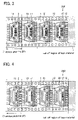
- FIG. 1 is a plan view showing a tape carrier for COF semiconductor device (before mounting semiconductor element) according to an embodiment of the present invention.
- FIG. 2 is a plan view showing the tape carrier of FIG. 1 on which a semiconductor element is mounted (semiconductor device), according to the embodiment of FIG. 1 of the present invention.
- FIG. 3 is a plan view showing a tape carrier for TCP semiconductor device (before mounting semiconductor element), according to another embodiment of the present invention.
- FIG. 4 is a plan view showing the tape carrier of FIG. 3 on which a semiconductor element is mounted (semiconductor device), according to the embodiment of FIG. 3 of the present invention.
- FIG. 5 is a cross-sectional view showing a COF semiconductor device according to an embodiment of the present invention, corresponding to the embodiment of FIGS. 1 and 2 .
- FIG. 6 is a cross-sectional view showing a TCP semiconductor device according to an embodiment of the present invention, corresponding to the embodiment of FIGS. 3 and 4 .
- FIG. 7 is a cross-sectional view showing a semiconductor module device according to an embodiment of the present invention, corresponding to the embodiment of FIG. 5 .
- FIG. 8 is a cross-sectional view showing a semiconductor module device according to an embodiment of the present invention, corresponding to the embodiment of FIG. 6 .
- FIG. 9 is a plan view showing a tape carrier for COF semiconductor device (before mounting semiconductor element), according to still another embodiment of the present invention.
- FIG. 10 is a plan view showing the tape carrier of FIG. 9 on which a semiconductor element is mounted (semiconductor device), according to the embodiment of FIG. 9 of the present invention.
- FIG. 11 is a plan view showing a COF semiconductor device according to yet another embodiment of the present invention.
- FIG. 12 is a plan view showing a COF semiconductor device according to still another embodiment of the present invention.
- FIG. 13 is a plan view showing a semiconductor element mounting step according to an embodiment of the present invention.
- FIG. 14 is a plan view showing a cutting-out step of a COF semiconductor device according to an embodiment of the present invention.
- FIG. 15 is a plan view showing a conventional tape carrier for COF semiconductor device (before mounting semiconductor element).
- FIG. 16 is a plan view showing a conventional COF semiconductor device.
- FIG. 17 is a plan view showing a conventional tape carrier for TCP semiconductor device (before mounting semiconductor element).
- FIG. 18 is a plan view showing a conventional TCP semiconductor device.
- FIG. 19 is a plan view showing another conventional tape carrier for COF semiconductor device (before mounting semiconductor element).
- FIG. 20 is a plan view showing a mounting step of a conventional semiconductor element.
- FIG. 21 is a plan view showing a cutting-out step of a conventional COF semiconductor device.
- FIGS. 1 to 4 show embodiments of a COF tape carrier, a TCP tape carrier, and a semiconductor device according to the present invention
- FIGS. 5 to 8 show cross-sectional views of a COF semiconductor device, a TCP semiconductor device, and a module.
- a tape carrier 100 used in the subject COF includes an insulative tape 1 as a base material, which is a flexible polyimide-type thin film 15 to 40 ⁇ m in thickness, and can be freely folded.
- the insulative tape 1 has a 8 to 18 ⁇ m thick copper foil or sputtered copper (wire pattern) laminated thereon by casting, sputtering (metalization technology) or the like.
- a tape carrier 200 used in the subject TCP includes a polyimide insulative tape 1 on which a copper foil is laminated through an adhesive 18 .
- the insulative tape 1 is provided with opening sections 16 in advance on a portion where the semiconductor element 21 is supposed to be mounted.
- Wire patterns 11 are protruded like cantilevers, and therefore their thickness are set to 18 ⁇ m or greater.
- a slit 17 is formed in advance in a fold-portion to be folded after the resulting semiconductor device is mounted to the liquid crystal panel or the like.
- the surface of the wire pattern 11 is coated with tin or gold.
- a solder resist 13 is applied to a junction between the wire patterns 11 and the semiconductor element 21 , and a pattern exposing section except for an external connection section 12 .
- the solder resist 13 is not applied to a mounting region 15 where the semiconductor element 21 is to be mounted, and a solder resist opening section 14 is formed instead.
- the coating layer is not illustrated in the figure.
- the insulative tape 1 of the thin film often has carriage-purpose openings called sprocket holes 2 which are formed at a 4.75 mm interval, and the tape pitch, which corresponds to the outer shape of the product, is generally set to a pitch of an integral multiple of that of the sprocket holes 2 .
- the tape is carried through the facilities of the production process on the basis of 1-pitch of the sprocket holes 2 . As a result, the part corresponding to the outer dimension pitch (an integral multiple) of a product is moved for each manufacturing step (in a step of processing/carrying a single device).
- the semiconductor element 21 is thereon provided with a protruding electrode called a bump 23 .
- the bump 23 is formed on the surface of the insulative tape 1 .
- the opening section 16 is formed in advance by penetrating through the tape on a portion of the insulative tape 1 where the semiconductor element 21 is to be mounted, and the bump 23 is bonded/mounted to the wire patterns 11 which are protruded like cantilevers. In this way, each wire of the wire patterns 11 is conducted to a bump 23 of a corresponding terminal of the semiconductor element 21 .
- the gap between the semiconductor element 21 and the tape carrier 100 which is generated after the semiconductor element 21 is bonded and mounted is sealed by a resin 22 injected thereto.
- each wire pattern 11 is conducted to a liquid crystal panel 24 , a printed circuit-board 25 or the like.
- the present embodiment reduces an unformed region (unnecessary region) of the insulative tape 1 which is irrelevant to the outer dimension of the COF semiconductor device or the TCP semiconductor device, thereby reducing material cost.
- FIGS. 15 to 18 show conventional COF and TCP tape carriers ( 500 , 600 ).
- the tape contains an unformed region (unnecessary region) 503 of the insulative tape 501 which is irrelevant to the outer dimension of the COF semiconductor device or the TCP semiconductor device. Such an unformed region causes wastes of material/processing cost, manufacturing performance, or the like.
- the unformed region (unnecessary region) of the insulative tape 1 which is irrelevant to the outer dimension of the COF semiconductor device or the TCP semiconductor device is cut. Therefore, the conventional problems of wastes of material/processing cost, manufacturing performance, or the like in the tape carriers ( 500 , 600 ) for a conventional COF or TCP semiconductor device due to an increase in tape pitch can be solved, and material cost of a tape carrier for a COF or TCP semiconductor device can be reduced to about 90% of that for the conventional structure (set to 5 pitch on average).
- FIG. 19 shows a tape carrier 700 for COP as another conventional example.
- the external connection sections 512 are oppositely provided so as to reduce the unformed region 503 , thereby reducing the tape pitch of the tape carrier 700 .
- Such minimization in tape pitch of the tape carrier 700 by oppositely disposing the external connection sections 512 may not always useful for various COFs of different shapes, that is, the directions of the components on the tape carrier 700 have to be changed for each type of COF according to its shape.
- the manufacturing is required to be carried out with switching operations for changing the directions of the respective components when they are mounted to the tape carrier 700 , according to the disposition direction of the COF.
- reduction in tape pitch of the tape carrier 700 and simplification of manufacturing process both need to be taken into account in the designing.
- the present invention does not require designing of the disposition direction of the components on the tape carrier according to the shape of COF.
- FIGS. 9 and 10 show a tape carrier 100 for a COF, and a semiconductor device, as embodiments of the present invention.
- the problems of wastes of material/processing cost, manufacturing performance, or the like of the tape carriers ( 500 , 600 ) for a conventional COF semiconductor device due to an increase in tape pitch can be eliminated, and material cost of a tape carrier for a COF semiconductor device can be reduced to about 85% of that for the conventional COF or TCP tape carrier (5 pitch on average).
- FIG. 11 shows a COF semiconductor device according to an embodiment of the present invention.
- the outer dimension of a COF semiconductor device in the carriage direction of the insulative tape 1 is reduced in a design process of the wire patterns 11 .
- the reduction of outer dimension may be performed by decreasing the pitch between wires, by changing the layout of wire patterns, or by changing the outer shape according to user specifications.
- the tape carrier 100 for a COP according to the present embodiment ensures an effect greater than that given by the tape carrier 100 of Embodiment 1 (the material cost is reduced to about 70%).
- FIG. 12 shows a COF semiconductor device as an embodiment of the present invention.
- the outer dimension of a COF semiconductor device in the carriage direction of the insulative tape 1 is reduced in a design process of the wire patterns 11 .
- the reduction of the outer dimension of the COF semiconductor device in the carriage direction of the insulative tape 1 in the present embodiment is greater than Embodiment 3.
- the tape carrier 100 for a COF according to the present embodiment ensures an effect greater than that given by the tape carrier 100 of Embodiment 1 and 3 (the material cost is reduced to 50%).
- FIG. 13 shows a manufacturing step (semiconductor element mounting step) for a COF semiconductor device as an embodiment of the present invention.
- the carriage pitch of the production apparatus is set to 1 pitch as shown in FIG. 20
- the tape pitch of the COF semiconductor device is set to an integral multiple.
- the manufacturing step (semiconductor element mounting step) for a COF semiconductor device according to the present embodiment corresponds to the manufacturing step for a tape carrier 100 for a COF according to Embodiment 1, but the described manner (semiconductor element mounting step) is also useful for Embodiment 3 and Embodiment 4.
- FIG. 14 shows a manufacturing step (semiconductor device cutting-out step) for a COF semiconductor device as an embodiment of the present invention.
- the COF semiconductor devices are cut out of the insulative tape 1 one by one as shown in FIG. 21 .
- the processing pitch for manufacturing the COF semiconductor devices is set to an integral multiple so that a plurality of COF semiconductor devices is processed at once.
- the step of cutting the COF semiconductor devices out of the insulative tape 1 a plurality (two) of COF semiconductor devices is cut at once, and the cutting pitch is set to an integral multiple (9) of the pitch interval (4.75 mm) of the sprocket hole 2 .
- the manufacturing step (semiconductor device cutting-out step) for a COF semiconductor device according to the present embodiment corresponds to the manufacturing step for a tape carrier 100 for COF according to Embodiment 1, but the described manner is also useful for Embodiment 3 and Embodiment 4.
- the tape pitch can be reduced to a value of an integral multiple X+a decimal Y (0 ⁇ Y ⁇ 1) of the pitch of the sprocket holes.
- 4 pitch+1 ⁇ 2 pitch half pitch
- the pitch for product that is the integral multiple X+a decimal Y (0 ⁇ Y ⁇ 1) pitch, also in the manufacturing step or the product cutting process for a COF or TCP.
- a tape carrier for a COF or TCP semiconductor device and a manufacturing method for a semiconductor device according to the present embodiment provide an effect of reducing an unformed region (unnecessary region) not included in the outer dimension of the COF or TCP semiconductor device by the following arrangement, thereby reducing material cost.
- the present embodiment arranges the manufacturing method for a semiconductor device having a semiconductor element bonded/mounted to a flexible wiring substrate such that the tape pitch of the semiconductor device is set to the integral multiple X+a decimal Y (0 ⁇ Y ⁇ 1) according to the outer dimension of the semiconductor device, thereby reducing an unformed region (unnecessary region) of the insulative tape which is irrelevant to the outer dimension of the semiconductor device.
- the present embodiment is applicable to a field of manufacturing of semiconductor devices formed of tape materials, such as the COF or TCP semiconductor devices, or its components, and can be further applicable to a field related to manufacturing of a product specified in length using a roll-type material.
- the present embodiment reduces the unformed region of the insulative tape 1 which is irrelevant to the outer dimension of the semiconductor device.
- the manufacturing method for a COF or TCP semiconductor device simultaneously processes a plurality of the semiconductor devices in the assembly processes such as semiconductor element mounting, resin sealing, or test, and a product pitch of the semiconductor device is set to an integral multiple of the pitch interval of sprocket holes.
- the semiconductor device or the semiconductor module device according to the present embodiment is manufactured using the foregoing tape carrier for a COF or TCP semiconductor device, or the foregoing manufacturing method for a semiconductor device.
- the unformed region (unnecessary region) of the semiconductor device which is irrelevant to the outer dimension of the semiconductor device can be reduced.
- the present embodiment provides an effect of producing a semiconductor device tape carrier, a manufacturing method for a semiconductor device, a semiconductor device, and a semiconductor module device with about 10% reduction in material cost.
- a tape carrier for a COF or TCP semiconductor device is preferably arranged so that, in a case where the outer dimension of the semiconductor device in the carriage direction of the insulative tape is reduced in a design process of the wire patterns, the setting of the decimal Y (0 ⁇ Y ⁇ 1) pitch is carried out in the same process so that the tape pitch for the COF or TCP semiconductor device tape carrier is set to: the integral multiple X+the decimal Y pitch (0 ⁇ Y ⁇ 1).
- an unformed region (unnecessary region) of the insulative tape which is irrelevant to the outer dimension of the semiconductor device can be reduced, and material cost can be reduced.
- the manufacturing method for a COF or TCP semiconductor device may simultaneously process a plurality of the semiconductor devices in the assembly processes such as semiconductor element mounting, resin sealing, or test, and a product pitch of the semiconductor device is set to an integral multiple of the pitch interval of sprocket holes.
- the manufacturing method may be carried out with a production facility having a plurality of the processing mechanisms for processing the semiconductor device so as to simultaneously process a plurality of the semiconductor devices.
- the manufacturing method for a COF or TCP semiconductor device may carry out a cutting-out step of the semiconductor device in which a plurality of the semiconductor devices are simultaneously cut out of the insulative tape into products, and an outer dimension or a product pitch in the cutting-out process of the semiconductor devices are set to an integral multiple of the pitch interval of the sprocket holes T
- the method uses a single set of cutting dies to simultaneously cut out a plurality of the semiconductor devices.
- the tape pitch of the tape carrier for a COF or TCP semiconductor device is set to an integral multiple X+a decimal Y (0 ⁇ Y ⁇ 1).
- an unformed region (unnecessary region) of the insulative tape which is irrelevant to the outer dimension of the COF or TCP semiconductor device is reduced, and material cost for producing a semiconductor device or a semiconductor module device can be reduced.
- a semiconductor device tape carrier comprises an insulative tape of a thin film on which a plurality of wire patterns is provided; a semiconductor element; and an insulative resin which seals the semiconductor element and the wire patterns under the semiconductor element in a state where the semiconductor element is conducted to the wire patterns, wherein: the sealed semiconductor element and the wire patterns conducted to each other form a semiconductor device, and a plurality of sprocket holes for carrying the insulative tape is formed at a predetermined interval in a longitudinal direction of the semiconductor device tape carrier, and in a case where an outer width of the semiconductor device in the longitudinal direction is greater than X times (X being a natural number) and not more than X+Y (0 ⁇ Y ⁇ 1) times of the predetermined interval of the sprocket holes, the wire patterns are provided at an interval of X+Y times of the predetermined interval of the sprocket holes.
- the semiconductor device tape carrier according to the present embodiment may be arranged so that, in a case where an outer width of the semiconductor device in the longitudinal direction is greater than X times (X being a natural number) and not more than X+(1 ⁇ 2) times of the predetermined interval of the sprocket holes, the wire patterns are provided at an interval of X+(1 ⁇ 2) times of the predetermined interval of the sprocket holes.
- the semiconductor device tape carrier according to the present embodiment may be arranged so that, in a case where an outer width of the semiconductor device in the longitudinal direction is greater than X times (X being a natural number) and not more than X+(1 ⁇ 4) times of the predetermined interval of the sprocket holes, the wire patterns are provided at an interval of X+(1 ⁇ 4) times of the predetermined interval of the sprocket holes.
- the semiconductor device tape carrier according to the present embodiment is preferably arranged so that the semiconductor device is a COF or a TCP.
- a manufacturing method for a semiconductor device according to the present embodiment produces a semiconductor device using the foregoing semiconductor device tape carrier.
- a semiconductor device according to the present embodiment is produced using the foregoing semiconductor device tape carrier.
- a semiconductor module device is produced using the foregoing semiconductor device.
Landscapes
- Wire Bonding (AREA)
Abstract
Description
Claims (12)
Applications Claiming Priority (2)
| Application Number | Priority Date | Filing Date | Title |
|---|---|---|---|
| JP2006244782A JP4283292B2 (en) | 2006-09-08 | 2006-09-08 | Tape carrier for semiconductor device and method for manufacturing semiconductor device |
| JP2006-244782 | 2006-09-08 |
Publications (2)
| Publication Number | Publication Date |
|---|---|
| US20080061432A1 US20080061432A1 (en) | 2008-03-13 |
| US7582976B2 true US7582976B2 (en) | 2009-09-01 |
Family
ID=39168730
Family Applications (1)
| Application Number | Title | Priority Date | Filing Date |
|---|---|---|---|
| US11/896,827 Active US7582976B2 (en) | 2006-09-08 | 2007-09-06 | Semiconductor device tape carrier, manufacturing method for semiconductor device, semiconductor device, and semiconductor module device |
Country Status (5)
| Country | Link |
|---|---|
| US (1) | US7582976B2 (en) |
| JP (1) | JP4283292B2 (en) |
| KR (1) | KR100955439B1 (en) |
| CN (1) | CN100543978C (en) |
| TW (1) | TWI343614B (en) |
Cited By (3)
| Publication number | Priority date | Publication date | Assignee | Title |
|---|---|---|---|---|
| US20080078502A1 (en) * | 2006-10-02 | 2008-04-03 | Castillo Wilfred L | Laminate |
| US20120314175A1 (en) * | 2011-06-09 | 2012-12-13 | Shenzhen China Star Oploelectronics Technology Co., Ltd. | Cof, cof carrier tape and drive circuit of liquid crystal television |
| US10256174B2 (en) | 2016-07-01 | 2019-04-09 | Samsung Electronics Co., Ltd. | Film type semiconductor package |
Families Citing this family (5)
| Publication number | Priority date | Publication date | Assignee | Title |
|---|---|---|---|---|
| JP5325684B2 (en) | 2009-07-15 | 2013-10-23 | ルネサスエレクトロニクス株式会社 | Semiconductor device |
| JP2011035178A (en) * | 2009-08-03 | 2011-02-17 | Hitachi High-Technologies Corp | Electronic component mounting apparatus |
| CN102237334A (en) * | 2011-06-09 | 2011-11-09 | 深圳市华星光电技术有限公司 | Chip on film (COF) and COF carrier tape |
| KR101957492B1 (en) * | 2012-12-26 | 2019-03-12 | 엘지디스플레이 주식회사 | Flexible drive integrated circuit and cutting equipment for drive integrated circuit thereof |
| JP6870043B2 (en) * | 2019-08-27 | 2021-05-12 | ルネサスエレクトロニクス株式会社 | Semiconductor device |
Citations (4)
| Publication number | Priority date | Publication date | Assignee | Title |
|---|---|---|---|---|
| JP2000323533A (en) | 1999-05-14 | 2000-11-24 | Sharp Corp | Method of manufacturing tape carrier and tape carrier type semiconductor device |
| JP2001110853A (en) | 1999-08-03 | 2001-04-20 | Mitsui Mining & Smelting Co Ltd | Manufacturing method of film carrier tape for mounting electronic components and manufacturing apparatus of film carrier tape for mounting electronic components |
| US20060097368A1 (en) * | 2004-11-11 | 2006-05-11 | Toshiharu Seko | Flexible wiring substrate, semiconductor device and electronic device using flexible wiring substrate, and fabricating method of flexible wiring substrate |
| US7442074B2 (en) * | 2005-11-29 | 2008-10-28 | Matsushita Electric Industrial Co., Ltd. | Wiring board and method for producing the same |
Family Cites Families (1)
| Publication number | Priority date | Publication date | Assignee | Title |
|---|---|---|---|---|
| JP4070135B2 (en) * | 2004-05-11 | 2008-04-02 | 沖電気工業株式会社 | Tape carrier, semiconductor device manufacturing method, and semiconductor device |
-
2006
- 2006-09-08 JP JP2006244782A patent/JP4283292B2/en not_active Expired - Fee Related
-
2007
- 2007-09-05 TW TW096133101A patent/TWI343614B/en active
- 2007-09-06 US US11/896,827 patent/US7582976B2/en active Active
- 2007-09-07 CN CNB2007101490991A patent/CN100543978C/en active Active
- 2007-09-07 KR KR1020070091090A patent/KR100955439B1/en not_active Expired - Fee Related
Patent Citations (5)
| Publication number | Priority date | Publication date | Assignee | Title |
|---|---|---|---|---|
| JP2000323533A (en) | 1999-05-14 | 2000-11-24 | Sharp Corp | Method of manufacturing tape carrier and tape carrier type semiconductor device |
| US6911729B1 (en) * | 1999-05-14 | 2005-06-28 | Sharp Kabushiki Kaisha | Tape carrier semiconductor device |
| JP2001110853A (en) | 1999-08-03 | 2001-04-20 | Mitsui Mining & Smelting Co Ltd | Manufacturing method of film carrier tape for mounting electronic components and manufacturing apparatus of film carrier tape for mounting electronic components |
| US20060097368A1 (en) * | 2004-11-11 | 2006-05-11 | Toshiharu Seko | Flexible wiring substrate, semiconductor device and electronic device using flexible wiring substrate, and fabricating method of flexible wiring substrate |
| US7442074B2 (en) * | 2005-11-29 | 2008-10-28 | Matsushita Electric Industrial Co., Ltd. | Wiring board and method for producing the same |
Cited By (4)
| Publication number | Priority date | Publication date | Assignee | Title |
|---|---|---|---|---|
| US20080078502A1 (en) * | 2006-10-02 | 2008-04-03 | Castillo Wilfred L | Laminate |
| US9944051B2 (en) * | 2006-10-02 | 2018-04-17 | Mead Johnson Nutrition Co. | Laminate |
| US20120314175A1 (en) * | 2011-06-09 | 2012-12-13 | Shenzhen China Star Oploelectronics Technology Co., Ltd. | Cof, cof carrier tape and drive circuit of liquid crystal television |
| US10256174B2 (en) | 2016-07-01 | 2019-04-09 | Samsung Electronics Co., Ltd. | Film type semiconductor package |
Also Published As
| Publication number | Publication date |
|---|---|
| TW200828467A (en) | 2008-07-01 |
| KR20080023196A (en) | 2008-03-12 |
| JP2008066605A (en) | 2008-03-21 |
| KR100955439B1 (en) | 2010-05-04 |
| CN101140918A (en) | 2008-03-12 |
| CN100543978C (en) | 2009-09-23 |
| TWI343614B (en) | 2011-06-11 |
| US20080061432A1 (en) | 2008-03-13 |
| JP4283292B2 (en) | 2009-06-24 |
Similar Documents
| Publication | Publication Date | Title |
|---|---|---|
| US7582976B2 (en) | Semiconductor device tape carrier, manufacturing method for semiconductor device, semiconductor device, and semiconductor module device | |
| US7671454B2 (en) | Tape carrier, semiconductor apparatus, and semiconductor module apparatus | |
| US6559524B2 (en) | COF-use tape carrier and COF-structured semiconductor device using the same | |
| CN101689535B (en) | Semiconductor device and its manufacturing method, and display and its manufacturing method | |
| US7833910B2 (en) | Film substrate, fabrication method thereof, and image display substrate | |
| KR100399379B1 (en) | Semiconductor device and process for manufacturing the same, liquid crystal module and process for mounting the same | |
| US7977805B2 (en) | Flexible wiring substrate, semiconductor device and electronic device using flexible wiring substrate, and fabricating method of flexible wiring substrate | |
| KR102942636B1 (en) | Flexible printed circuit board, cof module and electronic device comprising the same | |
| US20060054349A1 (en) | Cof film carrier tape and its manufacturing method | |
| US6744123B2 (en) | Film carrier tape for mounting electronic devices thereon and method of manufacturing the same | |
| JP2008177618A (en) | Flexible wiring board, and semiconductor device and electronic apparatus using the same | |
| US20070057369A1 (en) | Wiring board and method for manufacturing the same, and semiconductor device | |
| US20080063789A1 (en) | Tape substrate having reinforcement layer for tape packages | |
| JP2011155201A (en) | Tape carrier, tape carrier-type semiconductor device, and method of manufacturing tape carrier-type semiconductor device | |
| JPH03125444A (en) | Improved film carrier | |
| JP5184578B2 (en) | Printed wiring board | |
| JP2003142535A (en) | Flexible wiring substrate and method of manufacturing the same | |
| JP2008205172A (en) | Cof carrier tape, method of manufacturing cof carrier tape, and method of manufacturing cof semiconductor device | |
| JPH02177452A (en) | Metal single layer film carrier | |
| JPH08191123A (en) | Lead frame manufacturing method | |
| JPH04137590A (en) | Multilayer circuit board | |
| JP2001332590A (en) | Tape carrier type semiconductor device | |
| JP2001110851A (en) | Film carrier tape |
Legal Events
| Date | Code | Title | Description |
|---|---|---|---|
| AS | Assignment |
Owner name: SHARP KABUSHIKI KAISHA, JAPAN Free format text: ASSIGNMENT OF ASSIGNORS INTEREST;ASSIGNORS:SEKO, TOSHIHARU;TOYOSAWA, KENJI;REEL/FRAME:023573/0714;SIGNING DATES FROM 20070821 TO 20070823 |
|
| STCF | Information on status: patent grant |
Free format text: PATENTED CASE |
|
| FEPP | Fee payment procedure |
Free format text: PAYOR NUMBER ASSIGNED (ORIGINAL EVENT CODE: ASPN); ENTITY STATUS OF PATENT OWNER: SMALL ENTITY |
|
| FPAY | Fee payment |
Year of fee payment: 4 |
|
| FEPP | Fee payment procedure |
Free format text: PAYOR NUMBER ASSIGNED (ORIGINAL EVENT CODE: ASPN); ENTITY STATUS OF PATENT OWNER: SMALL ENTITY Free format text: PAYER NUMBER DE-ASSIGNED (ORIGINAL EVENT CODE: RMPN); ENTITY STATUS OF PATENT OWNER: SMALL ENTITY |
|
| FPAY | Fee payment |
Year of fee payment: 8 |
|
| AS | Assignment |
Owner name: SHENZHEN TOREY MICROELECTRONIC TECHNOLOGY CO. LTD., CHINA Free format text: ASSIGNMENT OF ASSIGNORS INTEREST;ASSIGNOR:SHARP KABUSHIKI KAISHA;REEL/FRAME:053754/0905 Effective date: 20200821 |
|
| FEPP | Fee payment procedure |
Free format text: ENTITY STATUS SET TO SMALL (ORIGINAL EVENT CODE: SMAL); ENTITY STATUS OF PATENT OWNER: SMALL ENTITY |
|
| MAFP | Maintenance fee payment |
Free format text: PAYMENT OF MAINTENANCE FEE, 12TH YR, SMALL ENTITY (ORIGINAL EVENT CODE: M2553); ENTITY STATUS OF PATENT OWNER: SMALL ENTITY Year of fee payment: 12 |