US7553720B2 - Non-volatile memory device and fabrication method thereof - Google Patents
Non-volatile memory device and fabrication method thereof Download PDFInfo
- Publication number
- US7553720B2 US7553720B2 US11/604,222 US60422206A US7553720B2 US 7553720 B2 US7553720 B2 US 7553720B2 US 60422206 A US60422206 A US 60422206A US 7553720 B2 US7553720 B2 US 7553720B2
- Authority
- US
- United States
- Prior art keywords
- insulator
- layer
- volatile memory
- memory device
- forming
- Prior art date
- Legal status (The legal status is an assumption and is not a legal conclusion. Google has not performed a legal analysis and makes no representation as to the accuracy of the status listed.)
- Active, expires
Links
- 238000000034 method Methods 0.000 title claims description 33
- 238000004519 manufacturing process Methods 0.000 title description 6
- 239000012212 insulator Substances 0.000 claims abstract description 54
- 229910021420 polycrystalline silicon Inorganic materials 0.000 claims abstract description 40
- 229920005591 polysilicon Polymers 0.000 claims abstract description 40
- 150000004767 nitrides Chemical class 0.000 claims abstract description 26
- 239000000758 substrate Substances 0.000 claims abstract description 23
- 229910052710 silicon Inorganic materials 0.000 claims abstract description 6
- 239000010703 silicon Substances 0.000 claims abstract description 6
- XUIMIQQOPSSXEZ-UHFFFAOYSA-N Silicon Chemical compound [Si] XUIMIQQOPSSXEZ-UHFFFAOYSA-N 0.000 claims abstract description 5
- IJGRMHOSHXDMSA-UHFFFAOYSA-N Atomic nitrogen Chemical compound N#N IJGRMHOSHXDMSA-UHFFFAOYSA-N 0.000 claims description 37
- GQPLMRYTRLFLPF-UHFFFAOYSA-N Nitrous Oxide Chemical compound [O-][N+]#N GQPLMRYTRLFLPF-UHFFFAOYSA-N 0.000 claims description 18
- 229910052757 nitrogen Inorganic materials 0.000 claims description 18
- 239000011521 glass Substances 0.000 claims description 16
- VYPSYNLAJGMNEJ-UHFFFAOYSA-N Silicium dioxide Chemical compound O=[Si]=O VYPSYNLAJGMNEJ-UHFFFAOYSA-N 0.000 claims description 13
- 229910021417 amorphous silicon Inorganic materials 0.000 claims description 9
- 239000001272 nitrous oxide Substances 0.000 claims description 9
- 239000012535 impurity Substances 0.000 claims description 4
- 238000000151 deposition Methods 0.000 claims description 3
- 239000011810 insulating material Substances 0.000 claims description 3
- 150000002500 ions Chemical class 0.000 claims description 3
- 230000001678 irradiating effect Effects 0.000 claims description 3
- 229910052814 silicon oxide Inorganic materials 0.000 claims description 3
- QVGXLLKOCUKJST-UHFFFAOYSA-N atomic oxygen Chemical group [O] QVGXLLKOCUKJST-UHFFFAOYSA-N 0.000 claims description 2
- 239000001301 oxygen Substances 0.000 claims description 2
- 229910052760 oxygen Inorganic materials 0.000 claims description 2
- 239000010410 layer Substances 0.000 description 88
- 230000015654 memory Effects 0.000 description 12
- 238000005229 chemical vapour deposition Methods 0.000 description 6
- 238000009413 insulation Methods 0.000 description 6
- 230000000903 blocking effect Effects 0.000 description 5
- 230000006870 function Effects 0.000 description 5
- 239000000377 silicon dioxide Substances 0.000 description 5
- QGZKDVFQNNGYKY-UHFFFAOYSA-N Ammonia Chemical compound N QGZKDVFQNNGYKY-UHFFFAOYSA-N 0.000 description 3
- 238000009616 inductively coupled plasma Methods 0.000 description 3
- 230000005641 tunneling Effects 0.000 description 3
- 238000010586 diagram Methods 0.000 description 2
- 238000005530 etching Methods 0.000 description 2
- 239000007789 gas Substances 0.000 description 2
- 239000002184 metal Substances 0.000 description 2
- 230000003647 oxidation Effects 0.000 description 2
- 238000007254 oxidation reaction Methods 0.000 description 2
- 239000011241 protective layer Substances 0.000 description 2
- 239000004065 semiconductor Substances 0.000 description 2
- 235000012239 silicon dioxide Nutrition 0.000 description 2
- 229910052581 Si3N4 Inorganic materials 0.000 description 1
- 230000002159 abnormal effect Effects 0.000 description 1
- 229910021529 ammonia Inorganic materials 0.000 description 1
- 239000012774 insulation material Substances 0.000 description 1
- 239000000463 material Substances 0.000 description 1
- 229910000069 nitrogen hydride Inorganic materials 0.000 description 1
- 238000000059 patterning Methods 0.000 description 1
- 230000003746 surface roughness Effects 0.000 description 1
Images


Classifications
-
- H—ELECTRICITY
- H01—ELECTRIC ELEMENTS
- H01L—SEMICONDUCTOR DEVICES NOT COVERED BY CLASS H10
- H01L29/00—Semiconductor devices adapted for rectifying, amplifying, oscillating or switching, or capacitors or resistors with at least one potential-jump barrier or surface barrier, e.g. PN junction depletion layer or carrier concentration layer; Details of semiconductor bodies or of electrodes thereof ; Multistep manufacturing processes therefor
- H01L29/66—Types of semiconductor device ; Multistep manufacturing processes therefor
- H01L29/68—Types of semiconductor device ; Multistep manufacturing processes therefor controllable by only the electric current supplied, or only the electric potential applied, to an electrode which does not carry the current to be rectified, amplified or switched
- H01L29/76—Unipolar devices, e.g. field effect transistors
- H01L29/772—Field effect transistors
- H01L29/78—Field effect transistors with field effect produced by an insulated gate
- H01L29/792—Field effect transistors with field effect produced by an insulated gate with charge trapping gate insulator, e.g. MNOS-memory transistors
-
- H—ELECTRICITY
- H01—ELECTRIC ELEMENTS
- H01L—SEMICONDUCTOR DEVICES NOT COVERED BY CLASS H10
- H01L29/00—Semiconductor devices adapted for rectifying, amplifying, oscillating or switching, or capacitors or resistors with at least one potential-jump barrier or surface barrier, e.g. PN junction depletion layer or carrier concentration layer; Details of semiconductor bodies or of electrodes thereof ; Multistep manufacturing processes therefor
- H01L29/40—Electrodes ; Multistep manufacturing processes therefor
- H01L29/401—Multistep manufacturing processes
- H01L29/4011—Multistep manufacturing processes for data storage electrodes
- H01L29/40117—Multistep manufacturing processes for data storage electrodes the electrodes comprising a charge-trapping insulator
-
- H—ELECTRICITY
- H01—ELECTRIC ELEMENTS
- H01L—SEMICONDUCTOR DEVICES NOT COVERED BY CLASS H10
- H01L29/00—Semiconductor devices adapted for rectifying, amplifying, oscillating or switching, or capacitors or resistors with at least one potential-jump barrier or surface barrier, e.g. PN junction depletion layer or carrier concentration layer; Details of semiconductor bodies or of electrodes thereof ; Multistep manufacturing processes therefor
- H01L29/40—Electrodes ; Multistep manufacturing processes therefor
- H01L29/41—Electrodes ; Multistep manufacturing processes therefor characterised by their shape, relative sizes or dispositions
- H01L29/423—Electrodes ; Multistep manufacturing processes therefor characterised by their shape, relative sizes or dispositions not carrying the current to be rectified, amplified or switched
- H01L29/42312—Gate electrodes for field effect devices
- H01L29/42316—Gate electrodes for field effect devices for field-effect transistors
- H01L29/4232—Gate electrodes for field effect devices for field-effect transistors with insulated gate
- H01L29/4234—Gate electrodes for transistors with charge trapping gate insulator
-
- H—ELECTRICITY
- H01—ELECTRIC ELEMENTS
- H01L—SEMICONDUCTOR DEVICES NOT COVERED BY CLASS H10
- H01L29/00—Semiconductor devices adapted for rectifying, amplifying, oscillating or switching, or capacitors or resistors with at least one potential-jump barrier or surface barrier, e.g. PN junction depletion layer or carrier concentration layer; Details of semiconductor bodies or of electrodes thereof ; Multistep manufacturing processes therefor
- H01L29/40—Electrodes ; Multistep manufacturing processes therefor
- H01L29/43—Electrodes ; Multistep manufacturing processes therefor characterised by the materials of which they are formed
- H01L29/49—Metal-insulator-semiconductor electrodes, e.g. gates of MOSFET
- H01L29/51—Insulating materials associated therewith
- H01L29/511—Insulating materials associated therewith with a compositional variation, e.g. multilayer structures
- H01L29/513—Insulating materials associated therewith with a compositional variation, e.g. multilayer structures the variation being perpendicular to the channel plane
Definitions
- the present invention relates to a non-volatile memory device and a fabrication method. More specifically, the present invention relates to a non-volatile memory device formed on a glass substrate, and a method for fabricating a non-volatile memory device.
- a non-volatile memory device may be classified into a floating-gate memory device and a charge-trapping memory device.
- the floating-gate memory device is a device for maintaining a memory by using a potential well.
- the charge-trapping memory device is a device for maintaining a memory by trapping charges in a trap region inside a nitride film or a trap region present in an interface between a nitride film and an insulator.
- a representative form of the charge-trapping memory device is a Silicon-Oxide-Nitride-Oxide-Silicon (SONOS) configuration.
- the SONOS configuration may include a sequential stack of a semiconductor substrate, an ONO configuration, and a gate electrode.
- the ONO configuration may include a sequential stack of a tunneling oxide film, a nitride film and a blocking oxide film.
- the tunneling oxide film may tunnel electrons into a trap region inside the nitride film or a trap region of an interface of the nitride film.
- the blocking oxide film may block charges from moving between the nitride film and the gate electrode.
- the trap region may store charges.
- Source/drain regions may be provided in the semiconductor substrate on either side of this stack.
- Such a configuration may include a sequential stack of the glass substrate, the ONO configuration, and the gate electrode.
- the glass substrate may include a protective layer, e.g., a buffer oxide film, thereon to protect the glass substrate.
- a polysilicon layer may be provided on the protective layer. Source/drain regions may be provided in the polysilicon layer on either side of this stack.
- Creation of the polysilicon layer may include crystallizing an amorphous polysilicon layer, e.g., by irradiating the amorphous polysilicon layer with a laser.
- surfaces of the polysilicon layers may be rough and non-uniform, which may result in a large leakage current being generated.
- a leakage current may be significantly increased due to the non-uniformity and roughness of the surfaces of the polysilicon layer. Therefore, such a non-volatile memory may function abnormally during programming/erasing operations.
- the present invention is therefore directed to a non-volatile memory device and fabrication method therefore, which substantially overcome one or more of the problems due to the limitations and disadvantages of the related art.
- a SiON layer which may be formed by, e.g., using a nitrous oxide (N 2 O) plasma, between the polysilicon layer and the ONO stack, and a fabrication method thereof.
- a non-volatile memory device including a buffer oxide film on a substrate, a polysilicon layer on the buffer oxide film, a silicon oxy-nitride (SiON) layer on the polysilicon layer, a first insulator on the SiON layer, a nitride film on the first insulator, a second insulator on the nitride film, an electrode on the second insulator, and a source/drain in the polysilicon layer.
- SiON silicon oxy-nitride
- the SiON layer and the first insulator may be formed in a same insulating material having varying degrees of nitrogen content.
- the SiON layer may be approximately 10 to 25 ⁇ thick, e.g., approximately 20 ⁇ thick.
- the first insulator may be approximately 20 to 40 ⁇ thick, e.g., approximately 30 ⁇ thick.
- the first insulator may be silicon dioxide (SiO 2 ).
- the nitride film may be approximately 50 to 100 ⁇ thick, e.g., approximately 80 ⁇ thick.
- the second insulator may be approximately 100 to 200 ⁇ thick, e.g., approximately 150 ⁇ thick.
- At least one of the above and other features and advantages of the present invention may be realized by providing a method for fabricating a non-volatile memory device, the method including forming a buffer oxide film on a substrate, forming a polysilicon layer on the buffer oxide film, forming a silicon oxy-nitride (SiON) layer on the polysilicon layer, forming a first insulator on the SiON layer, forming a nitride film on the first insulator, forming a second insulator on the nitride film, forming an electrode on the second insulator, and forming a source/drain by injecting impurity ions into an exposed region of the polysilicon layer.
- SiON silicon oxy-nitride
- Forming the polysilicon layer may include irradiating an amorphous silicon layer deposited on the buffer oxide film with a laser beam.
- Forming the SiON layer and the first insulator may include using a nitrous oxide plasma.
- Forming the SiON layer and the first insulator may include, after a predetermined amount of time, reducing a concentration of nitrogen in the plasma. The predetermined amount of time may be determined in accordance with a desired thickness of the SiON layer.
- Forming the SiON layer and the first insulator may include depositing an insulating material.
- the SiON layer may be formed with a thickness of approximately 10 to 25 ⁇ .
- the first insulator may be formed with a thickness of approximately 20 to 40 ⁇ .
- the first insulator may be formed of silicon oxide (siO 2 ).
- FIGS. 1A to FIG. 1H illustrate cross-sectional views of stages in a method for fabricating a non-volatile memory device according to an exemplary embodiment of the present invention.
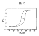
- FIG. 2 is a diagram showing a C-V characteristic of a non-volatile memory device according to an exemplary embodiment of the present invention.
- the non-volatile memory may include a glass substrate 100 , a buffer oxide film 101 , a polysilicon layer 103 , a SiON layer 104 , a first insulator 105 , a nitride film 106 , a second insulator 107 , an electrode 108 , a source 109 and a drain 110 .
- the first insulator 105 may serve as a tunneling oxide film
- the nitride film 106 may serve as a trapping film
- the second insulator 107 may serve as a blocking oxide film.
- Such a non-volatile memory of an exemplary embodiment of the present invention may reduce or eliminate surface roughness in the layer serving as the base for an ONO stack formed on a glass substrate.
- the non-volatile memory may reduce or eliminate a leakage current presently generated in such memories formed on a glass substrate, allowing the memory to function properly.
- FIGS. 1A to FIG. 1H a cross-sectional views of stages in a method for fabricating a non-volatile memory device according to an exemplary embodiment of the present invention.
- the buffer oxide film 101 may be deposited on the glass substrate 100 , e.g., using a chemical vapor deposition (CVD) process.
- the buffer oxide film 101 may be formed thickly enough to block impurities between the glass substrate and a non-volatile memory device to be formed later.
- the buffer oxide film 101 may have a thickness of approximately 3,000 ⁇ .
- an amorphous silicon layer 102 may be deposited on the buffer oxide film 101 , e.g., using a CVD process.
- the amorphous silicon layer 102 may have a thickness of approximately 500 ⁇ 600 ⁇ .
- the amorphous silicon layer 102 may be irradiated with a laser beam, as shown in FIG. 1B .
- a predetermined thickness of the amorphous silicon layer 102 may be changed into the polysilicon layer 103 as a result of the irradiation, as shown in FIG. 1C .
- this will be illustrated using only the polysilicon layer 103 .
- part of the thickness of the amorphous silicon layer may remain, i.e., both amorphous silicon layer and polysilicon may be present in layer 103 .
- an upper surface of the polysilicon layer 103 formed through irradiation may not be uniform, i.e., may be rough.
- the silicon oxy-nitride (SiON) layer 104 and the first insulator 105 may be sequentially formed on the polysilicon layer 103 , as shown in FIG. 1D .
- the first insulator 105 may be, e.g., silicon dioxide (SiO 2 ).
- the SiON layer 104 and the first insulator 105 may be formed in an inductively coupled plasma CVD apparatus using, e.g., a nitrous oxide (N 2 O) plasma.
- the operation may be performed at a low temperature, e.g., about 500° C. or less.
- the SiON layer 104 may be thinner than the first insulator 105 .
- the resultant SiON layer 104 may have a thickness of approximately 10 to 25 ⁇ , e.g., approximately 20 ⁇ .
- the first insulator 105 may have a thickness of approximately 20 to 40 ⁇ , e.g., approximately 30 ⁇ .
- the SiON layer 104 and the first insulator 105 may be sequentially formed using the same apparatus, and a concentration of nitrogen included in the insulation layer formed on the polysilicon may be reduced during processing.
- the concentration of nitrogen may decrease from a surface of the polysilicon layer 103 to the upper surface of the first insulator 105 by varying a concentration of nitrogen in the N 2 O plasma while carrying out the oxidation process.
- the nitrogen N 2 O plasma may be reduced to zero at some point in the process, in accordance with a desired thickness of the SiON layer 104 .
- the SiON layer 104 formed on the surface of the polysilicon layer 103 may include a high concentration of nitrogen, while the first insulator 105 formed on the SiON layer 104 may have little or no nitrogen.
- a concentration of nitrogen may be increased in the surface of the polysilicon layer 103 , forming Si 3 N 4 at the surface of the polysilicon layer 103 at a very rapid rate in the early stage of the oxidation process using the N 2 O plasma.
- the concentration of nitrogen in the plasma may be reduced, e.g., by substituting oxygen for the nitrogen, while the insulation layer 105 grows.
- the insulation layer may be classified into the SiON layer 104 and the first insulator 105 , based on the nitrogen concentration. For example, when an insulation layer is deposited in accordance with the above process to a thickness of 80 ⁇ , the insulation layer thinner than 40 ⁇ may become the SiON layer 104 , while the insulation layer thicker than 40 ⁇ may become the first insulator 105 , i.e., the SiO 2 layer, since the concentration of nitrogen may be nearly zero at a thickness of 40 ⁇ or more from the surface of the polysilicon.
- the layers 104 and 105 may be made from different materials and/or in different apparatuses. Further, while control of the nitrogen content may make the layers 104 and 105 clearly distinct, these layers may also have more of a gradient of nitrogen therethrough, such that the layers are non-distinct.
- Programming/erasing operations of the non-volatile memory on the glass substrate 100 having the SiON layer 104 and the first insulator 105 thereon, formed as above, may function normally, since a leakage current caused by the surface characteristic of the conventional polysilicon may be reduced or eliminated.
- the nitride film 106 may be formed on the first insulator 105 using, e.g., an inductively coupled plasma CVD apparatus.
- the nitride film 106 may be formed with a thickness of approximately 50 to 100 ⁇ , e.g., a thickness of approximately 80 ⁇ .
- the nitride film 106 may be formed using an ammonia (NH 3 ) gas or a nitrogen (N 2 ) gas.
- the nitride film 106 may store information by trapping charges in a trap region inside the nitride film 106 , an interfacial trap region between the first insulator 105 and the nitride film 106 , or an interfacial trap region between the nitride film 106 and the second insulator 107 , to be formed later.
- the second insulator 107 may be formed on the nitride film 106 , e.g., using an inductively coupled plasma CVD apparatus.
- the second insulator 107 may be formed with a thickness of approximately 100 to 200 ⁇ , e.g., approximately 150 ⁇ .
- the second insulator 107 may function as a blocking oxide film by blocking charges from moving between the gate electrode 108 and the nitride film 106 having a charge trap region in the non-volatile memory formed on the glass substrate.
- the metal electrode 108 may be formed by depositing and patterning a metal on the second insulator 107 , followed by carrying out a lithographic and an etching process, as shown in FIG. 1G .
- a source 109 and a drain 110 may be formed by carrying out a lithographic and an etching process to expose a portion of the polysilicon layer 103 , and injecting impurity ions into the exposed polysilicon layer 103 , as shown in FIG. 1H .
- FIG. 2 illustrates a diagram showing a C-V characteristic of a non-volatile memory device according to an exemplary embodiment of the present invention.
- the non-volatile memory device in accordance with an exemplary embodiment of the present invention may avoid abnormal programming/erasing characteristics arising from large leakage currents present due to a rough, non-uniform surface of the polysilicon layer formed by the conventional process, i.e., the non-volatile memory device according to an exemplary embodiment of the present invention may have a normal programming/erasing characteristic.
- a non-volatile memory device may be formed on a glass substrate with an ONO configuration and may normally function, with little or no leakage current. Also, the non-volatile memory device of the present invention may be widely employed in the various fields, since it is compatible with the SOG (System On Glass) technique.
- SOG System On Glass
Abstract
Description
Claims (10)
Applications Claiming Priority (2)
| Application Number | Priority Date | Filing Date | Title |
|---|---|---|---|
| KR2005-0114422 | 2005-11-28 | ||
| KR1020050114422A KR100719680B1 (en) | 2005-11-28 | 2005-11-28 | Non-volatile memory device and fabrication method thereof |
Publications (2)
| Publication Number | Publication Date |
|---|---|
| US20070122978A1 US20070122978A1 (en) | 2007-05-31 |
| US7553720B2 true US7553720B2 (en) | 2009-06-30 |
Family
ID=38088055
Family Applications (1)
| Application Number | Title | Priority Date | Filing Date |
|---|---|---|---|
| US11/604,222 Active 2027-03-20 US7553720B2 (en) | 2005-11-28 | 2006-11-27 | Non-volatile memory device and fabrication method thereof |
Country Status (2)
| Country | Link |
|---|---|
| US (1) | US7553720B2 (en) |
| KR (1) | KR100719680B1 (en) |
Families Citing this family (2)
| Publication number | Priority date | Publication date | Assignee | Title |
|---|---|---|---|---|
| KR100830329B1 (en) * | 2006-11-20 | 2008-05-19 | 삼성에스디아이 주식회사 | Non-volatile memory device and fabrication method thereof and apparatus of memory including thereof |
| KR100990534B1 (en) * | 2008-05-29 | 2010-10-29 | 주식회사 동부하이텍 | a nonvolatile semiconductor device, a fabricating method and a method for fabricating a flat panel display device embedding the nonvolatile semiconductor device |
Citations (8)
| Publication number | Priority date | Publication date | Assignee | Title |
|---|---|---|---|---|
| US20010004537A1 (en) * | 1999-12-18 | 2001-06-21 | Lee Sung Kwon | Method for fabricating thin film transistors |
| KR20010092958A (en) | 2000-03-28 | 2001-10-27 | 준 신 이 | Method of producing a thin film nonvolatile memory by using a buffer layer of Y2O3 and CeO2 |
| US6365320B1 (en) * | 1995-06-07 | 2002-04-02 | Advanced Micro Devices, Inc. | Process for forming anti-reflective film for semiconductor fabrication using extremely short wavelength deep ultraviolet photolithography |
| US20020163032A1 (en) * | 2001-05-03 | 2002-11-07 | Horng-Chih Lin | Nonvolatile memory and method of manufacturing the same |
| US20040053468A1 (en) * | 2002-09-12 | 2004-03-18 | Zhong Dong | Method for forming a protective buffer layer for high temperature oxide processing |
| US20050037550A1 (en) * | 2001-10-15 | 2005-02-17 | Myung-Koo Kang | Thin film transistor using polysilicon and a method for manufacturing the same |
| US7119865B2 (en) * | 2003-10-16 | 2006-10-10 | Lg.Philips Lcd Co., Ltd. | Transflective-type liquid crystal display device including projection seed pattern along same layer as the semiconductor layer |
| US20070029625A1 (en) * | 2005-08-04 | 2007-02-08 | Macronix International Co., Ltd. | Non-volatile memory semiconductor device having an oxide-nitride-oxide (ONO) top dielectric layer |
Family Cites Families (3)
| Publication number | Priority date | Publication date | Assignee | Title |
|---|---|---|---|---|
| KR100437453B1 (en) * | 2002-05-23 | 2004-06-23 | 삼성전자주식회사 | NAND-type non-volatile memory device having SONOS gate structure and method of forming the same |
| KR100988808B1 (en) * | 2003-12-18 | 2010-10-20 | 주식회사 하이닉스반도체 | Non-volatile memory device and method for fabrication of the same |
| KR100565757B1 (en) * | 2004-05-27 | 2006-03-29 | 동부아남반도체 주식회사 | Flash memory device and Fabricating method for the same |
-
2005
- 2005-11-28 KR KR1020050114422A patent/KR100719680B1/en active IP Right Grant
-
2006
- 2006-11-27 US US11/604,222 patent/US7553720B2/en active Active
Patent Citations (8)
| Publication number | Priority date | Publication date | Assignee | Title |
|---|---|---|---|---|
| US6365320B1 (en) * | 1995-06-07 | 2002-04-02 | Advanced Micro Devices, Inc. | Process for forming anti-reflective film for semiconductor fabrication using extremely short wavelength deep ultraviolet photolithography |
| US20010004537A1 (en) * | 1999-12-18 | 2001-06-21 | Lee Sung Kwon | Method for fabricating thin film transistors |
| KR20010092958A (en) | 2000-03-28 | 2001-10-27 | 준 신 이 | Method of producing a thin film nonvolatile memory by using a buffer layer of Y2O3 and CeO2 |
| US20020163032A1 (en) * | 2001-05-03 | 2002-11-07 | Horng-Chih Lin | Nonvolatile memory and method of manufacturing the same |
| US20050037550A1 (en) * | 2001-10-15 | 2005-02-17 | Myung-Koo Kang | Thin film transistor using polysilicon and a method for manufacturing the same |
| US20040053468A1 (en) * | 2002-09-12 | 2004-03-18 | Zhong Dong | Method for forming a protective buffer layer for high temperature oxide processing |
| US7119865B2 (en) * | 2003-10-16 | 2006-10-10 | Lg.Philips Lcd Co., Ltd. | Transflective-type liquid crystal display device including projection seed pattern along same layer as the semiconductor layer |
| US20070029625A1 (en) * | 2005-08-04 | 2007-02-08 | Macronix International Co., Ltd. | Non-volatile memory semiconductor device having an oxide-nitride-oxide (ONO) top dielectric layer |
Also Published As
| Publication number | Publication date |
|---|---|
| US20070122978A1 (en) | 2007-05-31 |
| KR100719680B1 (en) | 2007-05-17 |
Similar Documents
| Publication | Publication Date | Title |
|---|---|---|
| US7012299B2 (en) | Storage layer optimization of a nonvolatile memory device | |
| KR100894098B1 (en) | Nonvolatile memory device having fast erase speed and improoved retention charactericstics, and method of fabricating the same | |
| US7479425B2 (en) | Method for forming high-K charge storage device | |
| KR100890040B1 (en) | Non-volatile memory device having charge trapping layer and method of fabricating the same | |
| US7060594B2 (en) | Memory device and method of manufacturing including deuterated oxynitride charge trapping structure | |
| US20080121887A1 (en) | Non-volatile memory device and fabrication method thereof and memory apparatus including thereof | |
| US20070287253A1 (en) | Semiconductor memory device and manufacturing method thereof | |
| US6893920B2 (en) | Method for forming a protective buffer layer for high temperature oxide processing | |
| US7553720B2 (en) | Non-volatile memory device and fabrication method thereof | |
| JP2004040064A (en) | Nonvolatile memory and method of manufacturing the same | |
| US7880220B2 (en) | Non-volatile memory device and fabrication method of non-volatile memory device and memory apparatus including non-volatile memory device | |
| JP2002261175A (en) | Nonvolatile semiconductor memory and its manufacturing method | |
| JP4358504B2 (en) | Method for manufacturing nonvolatile semiconductor memory device | |
| US7919371B2 (en) | Method for fabricating non-volatile memory device with charge trapping layer | |
| US8604536B2 (en) | Semiconductor device and method of manufacturing the same | |
| US8110485B2 (en) | Nanocrystal silicon layer structures formed using plasma deposition technique, methods of forming the same, nonvolatile memory devices having the nanocrystal silicon layer structures, and methods of fabricating the nonvolatile memory devices | |
| US20080296743A1 (en) | Semiconductor device and method for fabricating the same | |
| JPH0992738A (en) | Semiconductor device and fabrication thereof | |
| US6620705B1 (en) | Nitriding pretreatment of ONO nitride for oxide deposition | |
| US6969689B1 (en) | Method of manufacturing an oxide-nitride-oxide (ONO) dielectric for SONOS-type devices | |
| US10026745B1 (en) | Semiconductor memory cell structure | |
| US20110215419A1 (en) | System and method for improving cmos compatible non volatile memory retention reliability | |
| KR100914292B1 (en) | Method of fabricating the charge trapping layer having Silicon nanocrystal, and nonvolatile memory device and method of manufacturing the nonvolatile memory device using the same | |
| US20090108332A1 (en) | Non-volatile memory device with charge trapping layer and method for fabricating the same | |
| JPH0334469A (en) | Manufacture of nonvolatile memory |
Legal Events
| Date | Code | Title | Description |
|---|---|---|---|
| AS | Assignment |
Owner name: SAMSUNG SDI CO., LTD., KOREA, REPUBLIC OF Free format text: ASSIGNMENT OF ASSIGNORS INTEREST;ASSIGNORS:CHOI, BYOUNG DEOG;LEE, KI YONG;CHUNG, HO KYOON;AND OTHERS;REEL/FRAME:018640/0325 Effective date: 20061124 |
|
| AS | Assignment |
Owner name: SAMSUNG MOBILE DISPLAY CO., LTD., KOREA, REPUBLIC OF Free format text: ASSIGNMENT OF ASSIGNORS INTEREST;ASSIGNOR:SAMSUNG SDI CO., LTD.;REEL/FRAME:021998/0771 Effective date: 20081212 Owner name: SAMSUNG MOBILE DISPLAY CO., LTD., KOREA, REPUBLIC Free format text: ASSIGNMENT OF ASSIGNORS INTEREST;ASSIGNOR:SAMSUNG SDI CO., LTD.;REEL/FRAME:021998/0771 Effective date: 20081212 Owner name: SAMSUNG MOBILE DISPLAY CO., LTD.,KOREA, REPUBLIC O Free format text: ASSIGNMENT OF ASSIGNORS INTEREST;ASSIGNOR:SAMSUNG SDI CO., LTD.;REEL/FRAME:021998/0771 Effective date: 20081212 |
|
| STCF | Information on status: patent grant |
Free format text: PATENTED CASE |
|
| FEPP | Fee payment procedure |
Free format text: PAYOR NUMBER ASSIGNED (ORIGINAL EVENT CODE: ASPN); ENTITY STATUS OF PATENT OWNER: LARGE ENTITY |
|
| FEPP | Fee payment procedure |
Free format text: PAYOR NUMBER ASSIGNED (ORIGINAL EVENT CODE: ASPN); ENTITY STATUS OF PATENT OWNER: LARGE ENTITY Free format text: PAYER NUMBER DE-ASSIGNED (ORIGINAL EVENT CODE: RMPN); ENTITY STATUS OF PATENT OWNER: LARGE ENTITY |
|
| AS | Assignment |
Owner name: SAMSUNG DISPLAY CO., LTD., KOREA, REPUBLIC OF Free format text: MERGER;ASSIGNOR:SAMSUNG MOBILE DISPLAY CO., LTD.;REEL/FRAME:029203/0001 Effective date: 20120827 |
|
| FPAY | Fee payment |
Year of fee payment: 4 |
|
| FPAY | Fee payment |
Year of fee payment: 8 |
|
| MAFP | Maintenance fee payment |
Free format text: PAYMENT OF MAINTENANCE FEE, 12TH YEAR, LARGE ENTITY (ORIGINAL EVENT CODE: M1553); ENTITY STATUS OF PATENT OWNER: LARGE ENTITY Year of fee payment: 12 |