US7539588B2 - Data carrier with detection means for detecting a change made of information stored with storing means - Google Patents
Data carrier with detection means for detecting a change made of information stored with storing means Download PDFInfo
- Publication number
- US7539588B2 US7539588B2 US10/519,592 US51959204A US7539588B2 US 7539588 B2 US7539588 B2 US 7539588B2 US 51959204 A US51959204 A US 51959204A US 7539588 B2 US7539588 B2 US 7539588B2
- Authority
- US
- United States
- Prior art keywords
- information
- circuit
- test
- test information
- memory device
- Prior art date
- Legal status (The legal status is an assumption and is not a legal conclusion. Google has not performed a legal analysis and makes no representation as to the accuracy of the status listed.)
- Expired - Lifetime, expires
Links
Images


Classifications
-
- G—PHYSICS
- G07—CHECKING-DEVICES
- G07F—COIN-FREED OR LIKE APPARATUS
- G07F7/00—Mechanisms actuated by objects other than coins to free or to actuate vending, hiring, coin or paper currency dispensing or refunding apparatus
- G07F7/08—Mechanisms actuated by objects other than coins to free or to actuate vending, hiring, coin or paper currency dispensing or refunding apparatus by coded identity card or credit card or other personal identification means
- G07F7/10—Mechanisms actuated by objects other than coins to free or to actuate vending, hiring, coin or paper currency dispensing or refunding apparatus by coded identity card or credit card or other personal identification means together with a coded signal, e.g. in the form of personal identification information, like personal identification number [PIN] or biometric data
- G07F7/1008—Active credit-cards provided with means to personalise their use, e.g. with PIN-introduction/comparison system
-
- G—PHYSICS
- G06—COMPUTING OR CALCULATING; COUNTING
- G06K—GRAPHICAL DATA READING; PRESENTATION OF DATA; RECORD CARRIERS; HANDLING RECORD CARRIERS
- G06K19/00—Record carriers for use with machines and with at least a part designed to carry digital markings
- G06K19/06—Record carriers for use with machines and with at least a part designed to carry digital markings characterised by the kind of the digital marking, e.g. shape, nature, code
- G06K19/067—Record carriers with conductive marks, printed circuits or semiconductor circuit elements, e.g. credit or identity cards also with resonating or responding marks without active components
- G06K19/07—Record carriers with conductive marks, printed circuits or semiconductor circuit elements, e.g. credit or identity cards also with resonating or responding marks without active components with integrated circuit chips
- G06K19/073—Special arrangements for circuits, e.g. for protecting identification code in memory
-
- G—PHYSICS
- G06—COMPUTING OR CALCULATING; COUNTING
- G06Q—INFORMATION AND COMMUNICATION TECHNOLOGY [ICT] SPECIALLY ADAPTED FOR ADMINISTRATIVE, COMMERCIAL, FINANCIAL, MANAGERIAL OR SUPERVISORY PURPOSES; SYSTEMS OR METHODS SPECIALLY ADAPTED FOR ADMINISTRATIVE, COMMERCIAL, FINANCIAL, MANAGERIAL OR SUPERVISORY PURPOSES, NOT OTHERWISE PROVIDED FOR
- G06Q20/00—Payment architectures, schemes or protocols
- G06Q20/30—Payment architectures, schemes or protocols characterised by the use of specific devices or networks
- G06Q20/34—Payment architectures, schemes or protocols characterised by the use of specific devices or networks using cards, e.g. integrated circuit [IC] cards or magnetic cards
- G06Q20/341—Active cards, i.e. cards including their own processing means, e.g. including an IC or chip
-
- G—PHYSICS
- G07—CHECKING-DEVICES
- G07F—COIN-FREED OR LIKE APPARATUS
- G07F7/00—Mechanisms actuated by objects other than coins to free or to actuate vending, hiring, coin or paper currency dispensing or refunding apparatus
- G07F7/08—Mechanisms actuated by objects other than coins to free or to actuate vending, hiring, coin or paper currency dispensing or refunding apparatus by coded identity card or credit card or other personal identification means
- G07F7/0806—Details of the card
- G07F7/0813—Specific details related to card security
- G07F7/082—Features insuring the integrity of the data on or in the card
Definitions
- the invention relates to a data carrier comprising a circuit, which circuit comprises the following components, namely first memory means, which are designed for modifiable storage of information, the information being modifiable by an ambient parameter of the circuit, which ambient parameter acts on the first memory means.
- the invention also relates to a circuit, which circuit comprises the following components, namely first memory means, which are designed for modifiable storage of information, the information being modifiable by an ambient parameter of the circuit, which ambient parameter acts on the first memory means.
- the known data carrier which is designed for contactless communication with a read/write station and which comprises the known circuit, comprises first memory means which are designed for modifiable storage of information.
- the data carrier also comprises an access control means and a bus connection between the first memory means and the access control means, wherein, in normal operation, the information stored in the first memory means may be modified by desired electrical accessing of the access control means via the bus connection to the first memory means.
- an ambient parameter acting on the first memory means such as for example a short-wave light or an electrical field or a high temperature.
- a modification of the stored information brought about in this way may lead to complete failure of the data carrier or to dangerous malfunctioning of the data carrier or may possibly even be exploited for criminal purposes.
- the first memory means comprise a test memory area, which is provided for storing test information, and second memory means are provided which are designed for unmodifiable storage of reference information, and detection means are provided, to which the test information which may be read out from the first memory means and the reference information which may be read out from the second memory means may be supplied and which are designed, with the aid of the read-out test information and the read-out reference information, to detect a modification of the originally stored test information brought about by an ambient parameter acting on the first memory means.
- the first memory means comprise a test memory area, which is provided for storing test information, and second memory means are provided which are designed for unmodifiable storage of reference information, and detection means are provided, to which the test information which may be read out from the first memory means and the reference information which may be read out from the second memory means may be supplied and which are designed, with the aid of the read-out test information and the read-out reference information, to detect a modification of the originally stored test information brought about by an ambient parameter acting on the first memory means.
- the advantage is thereby achieved that an unambiguous statement as to whether the information stored in the first memory means has or has not been modified by an ambient parameter, and consequently in relation to the invalidity or validity respectively of the information stored in the first memory means may be made in a reliable and reproducible manner.
- modification of the stored information which is caused unintentionally, i.e. accidentally by an ambient parameter modifying the originally stored information, or intentionally, i.e. for purely technical or even criminal reasons, may be detected virtually one hundred percent reliably because the test information and the information are stored together in the first memory means and therefore are jointly exposed to the ambient parameter acting on the first memory means and are jointly subject to a modification caused thereby.
- a solution according to the invention may for example be characterized in that the test information or the reference information are stored in encrypted manner for security reasons and that the detection means comprise decrypting means for decrypting at least one of the two information elements.
- a solution according to the invention may be characterized in that the detection means may be designed to compare a representation of the test information with a representation of the reference information, which two representations may be calculated by suitable calculating methods.
- the detection means may be designed to perform a so-called coincidence method.
- the detection means may be realized as correlator.
- the advantage is achieved that, during a testing state time period, as provided for example during or after production of the circuit, functioning of the detection means may be prevented.
- the advantage is achieved that functioning of the detection means may be started at a well-defined time and that this functioning of the detection means can no longer be cancelled once started, whereby, from this time onwards, any modification of the information stored in the first memory means brought about by an ambient parameter for whatever reason may be reliably detected.
- test information is represented by a bit sequence which comprises only bits with logical values which do not occur during production of the first memory means or are not present after a modification of the information stored in the first memory means brought about by the action of an ambient parameter on the first memory means, wherein it may be mentioned, for the sake of completeness, that in both cases each bit of the first memory means represents either a logical one or a logical zero.
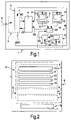
- FIG. 1 is a schematic representation, in the form of a block diagram, of a data carrier according to a first example of embodiment of the invention.
- FIG. 2 shows a data structure for storing information in first memory means of a data carrier according to the invention, in accordance with the first example of embodiment of the invention.
- FIG. 3 shows a data structure for storing information in the first memory means of a data carrier according to the invention, in accordance with a second example of embodiment of the invention.
- FIG. 1 shows a data carrier 1 , which is designed for contactless communication with a communications station not illustrated in FIG. 1 .
- the data carrier 1 is designed to receive a signal S from the communications station in contactless manner, wherein the signal is formed by a high-frequency carrier wave and wherein the data carrier 1 may be supplied with power by means of the signal S.
- interrogation information may be communicated from the communications station to the data carrier 1 by means of the signal S, wherein the signal exhibits amplitude modulation of the carrier wave.
- response information may be communicated from the data carrier 1 to the communications station by means of the signal S, wherein the signal S exhibits load modulation of the carrier wave which may be brought about by the data carrier 1 .
- phase or frequency modulation of the carrier wave may also be provided for communication purposes.
- the data carrier 1 comprises an electrical integrated circuit 2 .
- the circuit 2 comprises components of transceiver means 3 , which are designed to receive the signal S.
- the transceiver means 3 exhibit a transmission coil configuration, not shown in FIG. 1 , which is coupled to the circuit 2 , such that the signal S arising at the transmission coil configuration may be supplied to the circuit 2 .
- the transceiver means 3 are additionally designed, using the signal S, to generate a supply voltage V relative to a reference potential GND for the circuit 2 .
- the transceiver means 3 are additionally designed to demodulate the in this case modulated received signal S and to output interrogation data RD communicated by means of the modulated received signal S.
- the transceiver means 3 are additionally designed to receive response data AD and, for the purpose of transmitting the response data AD, for load modulation of the in this case unmodulated received signal S.
- the circuit 2 further comprises data processing means 4 , which take the form of a hard-wired logic circuit.
- the data processing means 4 may also take the form of a microcomputer.
- the data processing means 4 are designed to receive the interrogation data RD and to process the interrogation data RD and, as a function of the interrogation data RD, to generate the response data AD and to output the response data AD to the transceiver means 3 .
- the circuit 2 comprises first memory means 5 , which are designed for modifiable storage of information I, the information I being modifiable by an ambient parameter of the circuit 2 , which ambient parameter acts on the first memory means 5 .
- the first memory means 5 take the form of an EEPROM. It should be mentioned at this point that the first memory means 5 may, however, also take the form of other non-volatile read/write memories, such as for example an EPROM, a FLASH memory or a magnetic RAM. According to the invention, as soon as the first memory means 5 are exposed to an ambient parameter, such as for example a short-wave light, a high temperature of a relatively strong electromagnetic field, modification of the stored information I is brought about by this ambient parameter.
- an ambient parameter such as for example a short-wave light, a high temperature of a relatively strong electromagnetic field
- the first memory means 5 comprise a first user memory area 6 and a test memory area 7 .
- the test memory area 7 is provided for storage of test information TI.
- the user memory area 6 is provided for storage of user information UI.
- the information I storable in the first memory means 5 is consequently formed of the user information UI and the test information TI.
- the information I is represented by a large number of bits, wherein the bits are organized in a so-called sector-oriented data structure.
- FIG. 2 shows such a sector-oriented data structure for storing the information I in the first memory means 5 .
- the first user memory area 6 comprises a large number of data sectors, a first data sector 8 and a second data sector 9 and a third data sector 10 being shown as representatives thereof.
- Each of the large number of data sectors comprises a sector access control byte 11 and four sector data bytes 12 , 13 , 14 and 15 , which situation is illustrated by the first data sector 8 , acting as representative for the large number of data sectors.
- the sector access control byte 11 is provided for storing control data, by means of which access to the four sector data bytes 12 , 13 , 14 and 15 is enabled or prevented.
- the sector data bytes 12 , 13 , 14 and 15 are provided for storing user data for representing the user information UI.
- the test memory area 7 is formed by a test information byte, which is located at the highest memory address of the first memory means 5 . It should be mentioned in this context that any other memory address may also be provided therefore within the first memory means 5 . It should additionally be mentioned that the stored information I does not have to stored exclusively in the form of bytes, but may also be stored as logical nibbles each consisting of 4 bits or as logical words each consisting of 16 bits or by means of any other bit grouping.
- the circuit 2 illustrated in FIG. 1 further comprises two memory means 16 , which take the form of a ROM.
- the second memory means 16 comprise a second user memory area 17 and a reference memory area 18 .
- the second user memory area 17 is provided for the unmodifiable storage of constants, which are required for processing the data by means of the data processing means 4 or for generating response data AD, which will not be looked at in any more detail below, however.
- the reference memory area 18 is designed for unmodifiable storage of reference information RI.
- the constants and the reference information RI are represented by a large number of bits, which are organized in a data structure which is similar to the data structure in the first memory means 5 . It should be mentioned, however, that the data structure present within the second memory means 16 may in principle be independent, i.e. different from the data structure present in the first memory means 5 .
- the circuit 2 further comprises detection means 19 , to which the test information TI which may be read out from the first memory means 5 and the reference information RI which may be read out from the second memory means 16 may be supplied and which are designed, with the aid of the read-out test information TI and the read-out reference information RI, to detect a modification of the originally stored test information TI brought about by an ambient parameter acting on the first memory means 5 .
- the detection means 19 comprise first comparison means 20 , which are designed to access the first memory means 5 —specifically the test memory area 7 —for the purpose of reading out the test information TI.
- the first comparison means 20 are additionally designed to access the second memory means 16 —specifically the reference memory area 18 —for the purpose of reading out the reference information RI.
- the first comparison means 20 are additionally designed to compare the stored test information TI with the stored reference information RI.
- the detection means 19 are additionally designed to generate and output an indicator signal DS, which indicator signal DS is provided to indicate that modification of the originally stored test information TI brought about by an ambient parameter acting on the first memory means 5 has occurred, wherein the indicator signal DS is formed by a comparison result of the first comparison means 20 obtained as a result of the comparison of the test information TI with the reference information RI.
- the indicator signal DS may also take the form of a representation of the comparison result. It should additionally be mentioned that the indicator signal DS may also provide perpetual indication of the modification of the originally stored test information TI. This is the case, for example, when the indicator signal DS represents the content of a memory cell taking the form of a PROM or when the indicator signal DS represents a conductivity state of a single-use fuse. Detection of the modification of the originally stored test information TI may be performed in the present case each time a supply voltage V sufficient for data processing occurs, prior to said data processing. It should be mentioned, however, that said detection may also be performed periodically or non-periodically during data processing.
- the data processing means 4 are connected to the first memory means 5 and the second memory means 16 via a so-called bus connection B, wherein, with the aid of the bus connection B, the user information UI may be written to the first user memory area 6 of the first memory means 5 or read out from said first user memory area 6 and wherein information I representing the stored constants may be read out from the second user memory area 17 .
- the data processing means 4 are designed to prevent access to the first memory means 5 and/or the second memory means 16 .
- the data processing means 4 are designed to generate and output response data AD, which indicate that a modification of the originally stored test information TI brought about by an ambient parameter acting on the first memory means 5 has occurred.
- the data processing means 4 are stopped permanently from continuing to process data. Accordingly, the circuit 2 is designed to influence its operating behavior as a function of the indicator signal DS.
- the response data AD may be communicated to the read/write station by the communication means 3 , where they may be output, optionally in the form of visible display information, to a user of the data carrier 1 .
- the circuit 2 also comprises enabling means 21 , which are provided irreversibly to enable functioning of the detection means 19 .
- the enabling means 21 are designed, for this purpose, to generate and output a status signal SC, which may represent an enabling state or an inhibiting state.
- the first comparison means 20 of the detection means 19 are designed to receive the status signal SC, wherein, if the enabling state is represented, functioning of the detection means 19 is enabled and wherein, if the inhibiting state is represented, functioning of the detection means 19 is not enabled. Accordingly, the detection means 19 are designed to cooperate with the enabling means 21 .
- the enabling means 21 comprise a test signal generator 22 , which is designed to output a test signal SS to a first saw bow part 23 , which first saw bow part 23 constitutes a component of the circuit 2 .
- the enabling means 21 further comprise second comparison means 24 , which are designed to receive the test signal SS outputtable to the first saw bow part 23 .
- the second comparison means 24 are additionally connected to a second saw bow part 25 , and are designed to receive a comparison signal SS′ suppliable by means of the second saw bow part 25 of the circuit 2 .
- the second comparison means 24 are additionally designed to compare the test signal SS with the comparison signal SS′ and, if the test signal SS is identical to the comparison signal SS′, to output a status signal SC representing the inhibiting state. If the test signal SS is not identical to the comparison signal SS′, the second comparison means 24 are designed to output a status signal SC representing the enabling state.
- the first saw bow part 23 and the second saw bow part 25 are components of a “saw bow”, which saw bow, in the case of an integrated electrical circuit 2 arranged within a wafer, forms an electrically conductive connection between the first saw bow part 23 and the second saw bow part 25 within a sawing zone of the wafer, such that it may be established from the circuit 2 that the circuit 2 is arranged within the wafer and that tests may be performed which are designed not to be performable after separation of the circuit 2 from the wafer, specifically in the event of the circuit 2 being sawn out of the wafer.
- the saw bow is diced, such that, when the circuit 2 has been detached from the wafer, only the first saw bow part 23 and the second saw bow part 25 remain within the circuit 2 as components of the original saw bow. Accordingly, when the saw bow is intact, the comparison signal SS′ is formed by the test signal SS, whereas, when the saw bow has been cut through or destroyed, leaving only the first saw bow part 23 and the second saw bow part 25 within the circuit 2 , the two signals SS and SS′ are not identical to one another.
- Such a saw bow is known from patent document WO 02/09153 A2, the disclosure of which is deemed to be included herein.
- test memory area 7 from FIGS. 1 and 2 is distributed over each of the data sectors within user memory area 6 , such that each data sector has its “own” test information TI assigned to it, which is represented by a test information bit pair BP, BPA and BPB respectively, the first three data sectors 8 , 9 and 10 being illustrated as representatives of the large number of data sectors.
- test information TI which is represented by a test information bit pair BP, BPA and BPB respectively
- BP test information bit pair
- BPA and BPB test information bit pair
- the advantage is achieved that, even if the ambient parameter acts in isolated manner on one zone of the first memory means 5 , a modification of the originally stored test information TI, TIA or TIB respectively brought about by an ambient parameter acting on the first memory means 5 may be detected virtually one hundred percent reliably.
- more than two bits may be provided within each data sector 8 , 9 and 10 to represent the respective test information TI, TIA and TIB respectively and that the individual bits do not have to be arranged next to one another.
- test information which is represented by the bit sequence “01010110”, was stored in the test memory area 7 of the first memory means 5 .
- the four sector data bytes 12 , 13 , 14 and 15 are provided for storing user data representing the user information UI, which user data allow unambiguous identification of a user of the data carrier 1 .
- the user data may be stored in the user data memory area 6 by a service provider, which provides a user with the data carrier 1 , using a code for encrypted access to the four sector data bytes 12 , 13 , 14 and 15 . It should also be assumed that a bit sequence identical to the bit sequence stored in the test memory area 7 was stored in the reference memory area 18 .
- the circuit 2 was then severed from the wafer by sawing therefrom, wherein the saw bow was destroyed and the two saw bow parts 23 and 25 remain electrically isolated from one another within the circuit 2 . From this point in time, the first test information TI can no longer be modified.
- the user information UI required to identify the user is stored in the data carrier 1 , using the code submitted to the service provider by the semiconductor manufacturer, whereupon the data carrier 1 may be used to enable access to an area of an industrial company with restricted access.
- the data carrier 1 in circulation is exposed during use to a very wide range of environmental influences, which environmental influences are characterized by an ambient parameter of the data carrier 1 or the circuit 2 .
- environmental influences are characterized by an ambient parameter of the data carrier 1 or the circuit 2 .
- the data carrier 1 is brought inadvertently into the vicinity of a high-frequency welding apparatus, wherein a powerful high frequency field generated by means of the high-frequency welding apparatus deletes the contents of the first memory means 5 .
- the memory contents are returned to an “original state”, as was present originally after production of the first memory means 5 and in which the first memory means 5 comprise only bits which represent a logical one.
- the user who does not or indeed cannot notice this deletion of the contents of the first memory means 5 , introduces the data carrier 1 into a communications area of a read/write station, to gain access to the restricted access zone.
- the signal S output by the read/write station which signal S is formed by a high-frequency carrier wave, which is provided for communication with the data carrier 1 and for supplying the data carrier 1 with power, is received by the transceiver means 3 .
- the supply voltage V for the circuit 2 is generated by the transceiver means 3 .
- the test signal SS is generated by the test signal generator 22 and output to the first saw bow part 23 and the second comparison means 24 .
- the second comparison means 24 receive the comparison signal SS′, which does not match the test signal SS because the saw bow exists only in part within the circuit 2 .
- the second comparison means 24 then generate the status signal SC representing the enabling state and output this status signal SC to the first comparison means 20 .
- the status signal SC representing the enabling state results in the first comparison means 20 accessing the first memory means 5 and reading out the test information TI modified by the ambient parameter, which test information TI is represented at this point by the bit sequence “11111111”.
- the comparison means 20 also access the second memory means 16 and read out the originally stored reference information RI, which cannot be modified by the ambient parameter and which takes the form of the bit sequence “01010110”.
- the test information TI is then compared with the reference information RI by the first comparison means 20 , wherein the comparison reveals that a modification of the originally stored test information TI has been brought about by an ambient parameter acting on the first memory means, because the test information TI does not match the reference information RI.
- This detection of the modified test information TI is indicated by means of the indicator signal DS to the data processing means 4 , thereby putting a stop to any future processing in the data processing means 4 beyond the generation and outputting of response data AD, which response data AD represent the meaning of the indicator signal DS.
- the response data AD are communicated by the transceiver means 3 to the read/write station and are there interpreted to the effect that the data carrier 1 has become invalid because the originally stored test information TI has been modified and it may therefore be assumed that any other information I stored using the first memory means 5 has also in all probability been modified.
- circuit 2 in a data carrier 1 according to the invention has been described. It should be mentioned, however, that the circuit 2 according to the invention may also be used in a cell phone or a personal computer, for example.
- the circuit 2 may comprise a memory chip which includes the first memory means 5 , the second memory means 16 and the detection means 19 and that such a memory chip may be used, for example, in a so-called SIM module, which SIM module is currently used in cell phones to identify a user.
- SIM module which SIM module is currently used in cell phones to identify a user.
- the circuit 2 according to the invention may also comprise a microprocessor or interface chips, such that a microcontroller may be provided, for example, by means of the circuit 2 according to the invention.
- transceiver means 3 of the data carrier 1 may also take the form of an antenna configuration.
- transceiver means 3 may be designed for capacitive or optical communication.
- the data carrier 1 may also be designed for conventional contact communication.
- the data carrier 1 may also comprise its own power supply, which may take the form for example of at least one battery or one solar cell configuration.
- the enabling means 21 may take the form of a bit of a once-programmable PROM memory cell, wherein the PROM memory cell is programmed after completion of manufacturing and testing of the circuit 2 and prior to delivery of the circuit 2 to a customer. A logical value represented by this bit constitutes the state of the enabling means 21 which enables functioning of the detection means 19 .
- a bit pattern may also be provided instead of a single bit. If the second memory means 16 take the form of a PROM, at least one memory cell of this PROM may also be used to provide the enabling means 21 .
- the enabling means 21 take the form of once-programmable means, such as for example a PROM or a fuse
- the enabling means 21 may be programmed to enable the detection means 19 not by a manufacturer of the circuit 2 but by a data carrier manufacturer, who produces the data carrier 1 using the circuit 2 , or by a service provider, which delivers the data carrier 1 to an end user.
- the enabling means 21 may take the form of a fuse provided in the circuit 2 , wherein the fuse is fused prior to delivery of the circuit 2 to a customer and wherein the fused state of the fuse, i.e. the non-conductive state of the fuse, constitutes the state of the enabling means 21 which enables functioning of the detection means 19 .
- the second memory area 16 may be present, like the data processing means 4 , as part of a hard-wired logic circuit.
- the second memory means 16 may also take the form of a program memory of a microcomputer, wherein the reference information RI may also take the form of part of a program code.
- the second memory means 16 may be provided solely for storage of the reference information RI.
- test information TI and the reference information RI may be read out from the relevant memory means 5 and 16 using the data processing means 4 and supplied to the detection means 19 .
- the indicator signal DS may also be outputtable to the two memory means 5 and 16 and that at least one of the two memory means 5 and 16 may be designed to influence its accessibility as a function of the indicator signal DS.
- One possible embodiment of the invention may be characterized in that access is no longer possible to either of the memory means 5 and 16 when the indicator signal DS is present, indicating a modification of the originally stored test information TI.
- the indicator signal DS may also be outputtable to the transceiver means 3 and that the transceiver means 3 may be designed to influence their communicating capacity as a function of the indicator signal DS.
- hardware-enclosed memory areas may be provided for in each case one application and that each of these memory areas may comprise its own test information TI.
Landscapes
- Engineering & Computer Science (AREA)
- General Physics & Mathematics (AREA)
- Physics & Mathematics (AREA)
- Computer Security & Cryptography (AREA)
- Microelectronics & Electronic Packaging (AREA)
- Business, Economics & Management (AREA)
- Computer Hardware Design (AREA)
- Theoretical Computer Science (AREA)
- Accounting & Taxation (AREA)
- General Business, Economics & Management (AREA)
- Strategic Management (AREA)
- Computer Networks & Wireless Communication (AREA)
- General Engineering & Computer Science (AREA)
- Storage Device Security (AREA)
- Burglar Alarm Systems (AREA)
- Techniques For Improving Reliability Of Storages (AREA)
- Inspection Of Paper Currency And Valuable Securities (AREA)
- Cash Registers Or Receiving Machines (AREA)
- Near-Field Transmission Systems (AREA)
Applications Claiming Priority (3)
| Application Number | Priority Date | Filing Date | Title |
|---|---|---|---|
| EP02100761.2 | 2002-06-28 | ||
| EP02100761 | 2002-06-28 | ||
| PCT/IB2003/002022 WO2004003838A1 (en) | 2002-06-28 | 2003-05-16 | Data carrier with detection means for detecting a change made of information stored with storing means |
Publications (2)
| Publication Number | Publication Date |
|---|---|
| US20050240371A1 US20050240371A1 (en) | 2005-10-27 |
| US7539588B2 true US7539588B2 (en) | 2009-05-26 |
Family
ID=29797284
Family Applications (1)
| Application Number | Title | Priority Date | Filing Date |
|---|---|---|---|
| US10/519,592 Expired - Lifetime US7539588B2 (en) | 2002-06-28 | 2003-05-16 | Data carrier with detection means for detecting a change made of information stored with storing means |
Country Status (8)
| Country | Link |
|---|---|
| US (1) | US7539588B2 (de) |
| EP (1) | EP1520252B1 (de) |
| JP (1) | JP2005531841A (de) |
| CN (1) | CN100347727C (de) |
| AT (1) | ATE450836T1 (de) |
| AU (1) | AU2003230128A1 (de) |
| DE (1) | DE60330343D1 (de) |
| WO (1) | WO2004003838A1 (de) |
Cited By (1)
| Publication number | Priority date | Publication date | Assignee | Title |
|---|---|---|---|---|
| DE102017116280A1 (de) * | 2017-07-19 | 2019-01-24 | Infineon Technologies Ag | Speicheranordnung |
Families Citing this family (5)
| Publication number | Priority date | Publication date | Assignee | Title |
|---|---|---|---|---|
| AU2005215811A1 (en) | 2004-02-17 | 2005-09-01 | Cook Biotech Incorporated | Medical devices and methods for applying bolster material |
| EP2385374B2 (de) | 2010-05-05 | 2018-02-28 | Zora Biosciences OY | Lipidomik-Biomarker für Atherosklerose und kardiovaskuläre Erkrankung |
| CN102279919A (zh) * | 2010-06-13 | 2011-12-14 | 中兴通讯股份有限公司 | 筛选修复高频卡片的方法及阅读器 |
| CN103135008B (zh) * | 2011-12-05 | 2016-01-20 | 财团法人资讯工业策进会 | 电力异常侦测装置及其电力异常侦测方法 |
| JP2015052951A (ja) * | 2013-09-06 | 2015-03-19 | 独立行政法人産業技術総合研究所 | セキュリティ強化装置 |
Citations (10)
| Publication number | Priority date | Publication date | Assignee | Title |
|---|---|---|---|---|
| DE4205567A1 (de) * | 1992-02-22 | 1993-08-26 | Philips Patentverwaltung | Verfahren zum steuern des zugriffs auf einen speicher sowie anordnung zur durchfuehrung des verfahrens |
| JPH05265866A (ja) * | 1992-03-19 | 1993-10-15 | Csk Corp | 外部romのセキュリティシステム |
| US5471045A (en) | 1991-05-06 | 1995-11-28 | Gemplus Card International | Smart card locking process |
| US20010028691A1 (en) * | 2000-03-03 | 2001-10-11 | Martin Posch | Data carrier having means for synchronization with a received data stream |
| FR2810138A1 (fr) | 2000-06-08 | 2001-12-14 | Bull Cp8 | Procede de stockage securise d'une donnee sensible dans une memoire d'un systeme embarque a puce electronique, notamment d'une carte a puce, et systeme embarque mettant en oeuvre le procede |
| WO2002009153A2 (en) * | 2000-07-21 | 2002-01-31 | Koninklijke Philips Electronics N.V. | Method of fabricating integrated circuits, providing improved so-called 'saw bow' conductive tracks |
| US20030043896A1 (en) * | 2001-08-31 | 2003-03-06 | Koninklijke Philips Electronics N.V. | Device for and method of determining the quality of a data signal |
| US6800894B1 (en) * | 1998-12-11 | 2004-10-05 | Seiko Epson Corporation | Semiconductor devices, circuit substrates and electronic devices |
| US20060155882A1 (en) * | 2003-06-05 | 2006-07-13 | Koninklijke Philips Electronics N.V. | Integrity control for data stored in a non-volatile memory |
| US7232983B2 (en) * | 2002-11-22 | 2007-06-19 | Nxp B.V. | Circuit arrangement with non-volatile memory module and method for registering light-attacks on the non-volatile memory module |
Family Cites Families (3)
| Publication number | Priority date | Publication date | Assignee | Title |
|---|---|---|---|---|
| JPS5265866A (en) * | 1975-11-28 | 1977-05-31 | Matsushita Electric Works Ltd | Circuit breaker |
| GB2205186B (en) * | 1987-05-23 | 1991-02-13 | Motorola Inc | Memory cards |
| EP1197826B1 (de) * | 2000-09-18 | 2003-12-10 | Kabushiki Kaisha Toshiba | Gesicherte tragbare elektronische Vorrichtung |
-
2003
- 2003-05-16 EP EP03722971A patent/EP1520252B1/de not_active Expired - Lifetime
- 2003-05-16 CN CNB038150824A patent/CN100347727C/zh not_active Expired - Lifetime
- 2003-05-16 US US10/519,592 patent/US7539588B2/en not_active Expired - Lifetime
- 2003-05-16 AT AT03722971T patent/ATE450836T1/de not_active IP Right Cessation
- 2003-05-16 JP JP2004517024A patent/JP2005531841A/ja active Pending
- 2003-05-16 AU AU2003230128A patent/AU2003230128A1/en not_active Abandoned
- 2003-05-16 DE DE60330343T patent/DE60330343D1/de not_active Expired - Lifetime
- 2003-05-16 WO PCT/IB2003/002022 patent/WO2004003838A1/en not_active Ceased
Patent Citations (13)
| Publication number | Priority date | Publication date | Assignee | Title |
|---|---|---|---|---|
| US5471045A (en) | 1991-05-06 | 1995-11-28 | Gemplus Card International | Smart card locking process |
| US5467081A (en) * | 1992-02-22 | 1995-11-14 | U.S. Philips Corporation | Datacarriers with separate storage of read and write-inhibited memory locations |
| DE4205567A1 (de) * | 1992-02-22 | 1993-08-26 | Philips Patentverwaltung | Verfahren zum steuern des zugriffs auf einen speicher sowie anordnung zur durchfuehrung des verfahrens |
| JPH05265866A (ja) * | 1992-03-19 | 1993-10-15 | Csk Corp | 外部romのセキュリティシステム |
| US6800894B1 (en) * | 1998-12-11 | 2004-10-05 | Seiko Epson Corporation | Semiconductor devices, circuit substrates and electronic devices |
| US20010028691A1 (en) * | 2000-03-03 | 2001-10-11 | Martin Posch | Data carrier having means for synchronization with a received data stream |
| FR2810138A1 (fr) | 2000-06-08 | 2001-12-14 | Bull Cp8 | Procede de stockage securise d'une donnee sensible dans une memoire d'un systeme embarque a puce electronique, notamment d'une carte a puce, et systeme embarque mettant en oeuvre le procede |
| US20020108051A1 (en) * | 2000-06-08 | 2002-08-08 | Nicolas Fougeroux | Method for secure storage of sensitive data in a silicon chip integrated system storage in particular a smart card and integrated system therefor |
| WO2002009153A2 (en) * | 2000-07-21 | 2002-01-31 | Koninklijke Philips Electronics N.V. | Method of fabricating integrated circuits, providing improved so-called 'saw bow' conductive tracks |
| US6475817B2 (en) * | 2000-07-21 | 2002-11-05 | Koninklijke Philips Electronics N.V. | Method of fabricating integrated circuits, providing improved so-called saw bows |
| US20030043896A1 (en) * | 2001-08-31 | 2003-03-06 | Koninklijke Philips Electronics N.V. | Device for and method of determining the quality of a data signal |
| US7232983B2 (en) * | 2002-11-22 | 2007-06-19 | Nxp B.V. | Circuit arrangement with non-volatile memory module and method for registering light-attacks on the non-volatile memory module |
| US20060155882A1 (en) * | 2003-06-05 | 2006-07-13 | Koninklijke Philips Electronics N.V. | Integrity control for data stored in a non-volatile memory |
Cited By (2)
| Publication number | Priority date | Publication date | Assignee | Title |
|---|---|---|---|---|
| DE102017116280A1 (de) * | 2017-07-19 | 2019-01-24 | Infineon Technologies Ag | Speicheranordnung |
| DE102017116280B4 (de) | 2017-07-19 | 2024-02-22 | Infineon Technologies Ag | Speicheranordnung |
Also Published As
| Publication number | Publication date |
|---|---|
| WO2004003838A1 (en) | 2004-01-08 |
| DE60330343D1 (de) | 2010-01-14 |
| AU2003230128A1 (en) | 2004-01-19 |
| CN100347727C (zh) | 2007-11-07 |
| ATE450836T1 (de) | 2009-12-15 |
| JP2005531841A (ja) | 2005-10-20 |
| EP1520252A1 (de) | 2005-04-06 |
| EP1520252B1 (de) | 2009-12-02 |
| US20050240371A1 (en) | 2005-10-27 |
| CN1666225A (zh) | 2005-09-07 |
Similar Documents
| Publication | Publication Date | Title |
|---|---|---|
| US8074888B2 (en) | Terminal, method of checking conformity of at least one removable battery of an electronic payment terminal, and the corresponding removable battery and computer program product | |
| US8250288B2 (en) | Flash memory storage system and controller and data protection method thereof | |
| JP2014203719A (ja) | 車載バッテリー管理システム | |
| KR20000070856A (ko) | 최소 전압 무선 주파수 식별 장치 및 방법 | |
| WO2006083468A2 (en) | Radio frequency fingerprinting to detect fraudulent radio frequency identification tags | |
| CN202584165U (zh) | 一种ic卡生产测试系统 | |
| JP2009505266A (ja) | 不揮発性メモリモジュールを有する回路装置、およびこの不揮発性メモリモジュールに対する攻撃を記録する方法 | |
| CN114600121A (zh) | 具有隐私模式的射频识别集成电路 | |
| CN101685035B (zh) | 一种sim卡温度检测方法及装置、sim卡 | |
| US7539588B2 (en) | Data carrier with detection means for detecting a change made of information stored with storing means | |
| US20050121898A1 (en) | Authenticity tag and method for operating an authenticity tag | |
| US20100013631A1 (en) | Alarm recognition | |
| FR2670595A1 (fr) | Carte a circuit integre. | |
| EP1877988B1 (de) | Elektronisches artikelüberwachungssystem | |
| CN102129593B (zh) | 适于检测通过传送能量进行的攻击的电子部件 | |
| US20110078455A1 (en) | Communication device, communication method, information processing device, information processing method, program, and communication system | |
| CN104463022A (zh) | 一种具备自保护功能的硬件设备 | |
| US20090095955A1 (en) | Semiconductor integrated circuit and testing method thereof | |
| JP6009854B2 (ja) | Icカード、携帯可能電子装置、及びicカードの制御プログラム | |
| US8918610B2 (en) | Protection of chips against attacks | |
| CN101685505B (zh) | 无线射频识别电子卷标和具有其的电子装置 | |
| CN117785590B (zh) | 芯片及芯片数据保护方法 | |
| CN117712521B (zh) | 新旧电池识别方法和设备 | |
| CN110457970A (zh) | 一种rfid芯片上存储器的自校验方法 | |
| CN114416432B (zh) | 一种芯片安全启动检测方法、装置、设备及介质 |
Legal Events
| Date | Code | Title | Description |
|---|---|---|---|
| AS | Assignment |
Owner name: KONINKLIJKE PHILIPS ELECTRONICS N.V., NETHERLANDS Free format text: ASSIGNMENT OF ASSIGNORS INTEREST;ASSIGNORS:POSCH, MARTIN;HAAR, HELMUT;REEL/FRAME:016806/0010 Effective date: 20020628 |
|
| AS | Assignment |
Owner name: NXP B.V., NETHERLANDS Free format text: ASSIGNMENT OF ASSIGNORS INTEREST;ASSIGNOR:KONINKLIJKE PHILIPS ELECTRONICS N.V.;REEL/FRAME:019719/0843 Effective date: 20070704 Owner name: NXP B.V.,NETHERLANDS Free format text: ASSIGNMENT OF ASSIGNORS INTEREST;ASSIGNOR:KONINKLIJKE PHILIPS ELECTRONICS N.V.;REEL/FRAME:019719/0843 Effective date: 20070704 |
|
| STCF | Information on status: patent grant |
Free format text: PATENTED CASE |
|
| FPAY | Fee payment |
Year of fee payment: 4 |
|
| AS | Assignment |
Owner name: MORGAN STANLEY SENIOR FUNDING, INC., MARYLAND Free format text: SECURITY AGREEMENT SUPPLEMENT;ASSIGNOR:NXP B.V.;REEL/FRAME:038017/0058 Effective date: 20160218 |
|
| AS | Assignment |
Owner name: MORGAN STANLEY SENIOR FUNDING, INC., MARYLAND Free format text: CORRECTIVE ASSIGNMENT TO CORRECT THE REMOVE APPLICATION 12092129 PREVIOUSLY RECORDED ON REEL 038017 FRAME 0058. ASSIGNOR(S) HEREBY CONFIRMS THE SECURITY AGREEMENT SUPPLEMENT;ASSIGNOR:NXP B.V.;REEL/FRAME:039361/0212 Effective date: 20160218 |
|
| FPAY | Fee payment |
Year of fee payment: 8 |
|
| AS | Assignment |
Owner name: MORGAN STANLEY SENIOR FUNDING, INC., MARYLAND Free format text: CORRECTIVE ASSIGNMENT TO CORRECT THE REMOVE APPLICATION 12681366 PREVIOUSLY RECORDED ON REEL 039361 FRAME 0212. ASSIGNOR(S) HEREBY CONFIRMS THE SECURITY AGREEMENT SUPPLEMENT;ASSIGNOR:NXP B.V.;REEL/FRAME:042762/0145 Effective date: 20160218 Owner name: MORGAN STANLEY SENIOR FUNDING, INC., MARYLAND Free format text: CORRECTIVE ASSIGNMENT TO CORRECT THE REMOVE APPLICATION 12681366 PREVIOUSLY RECORDED ON REEL 038017 FRAME 0058. ASSIGNOR(S) HEREBY CONFIRMS THE SECURITY AGREEMENT SUPPLEMENT;ASSIGNOR:NXP B.V.;REEL/FRAME:042985/0001 Effective date: 20160218 |
|
| AS | Assignment |
Owner name: NXP B.V., NETHERLANDS Free format text: CHANGE OF NAME;ASSIGNOR:PHILIPS SEMICONDUCTORS INTERNATIONAL B.V.;REEL/FRAME:043951/0436 Effective date: 20060929 Owner name: PHILIPS SEMICONDUCTORS INTERNATIONAL B.V., NETHERL Free format text: ASSIGNMENT OF ASSIGNORS INTEREST;ASSIGNOR:KONINKLIJKE PHILIPS ELECTRONICS N.V.;REEL/FRAME:043955/0001 Effective date: 20060928 |
|
| AS | Assignment |
Owner name: NXP B.V., NETHERLANDS Free format text: RELEASE BY SECURED PARTY;ASSIGNOR:MORGAN STANLEY SENIOR FUNDING, INC.;REEL/FRAME:050745/0001 Effective date: 20190903 |
|
| AS | Assignment |
Owner name: MORGAN STANLEY SENIOR FUNDING, INC., MARYLAND Free format text: CORRECTIVE ASSIGNMENT TO CORRECT THE REMOVE APPLICATION 12298143 PREVIOUSLY RECORDED ON REEL 042985 FRAME 0001. ASSIGNOR(S) HEREBY CONFIRMS THE SECURITY AGREEMENT SUPPLEMENT;ASSIGNOR:NXP B.V.;REEL/FRAME:051029/0001 Effective date: 20160218 Owner name: MORGAN STANLEY SENIOR FUNDING, INC., MARYLAND Free format text: CORRECTIVE ASSIGNMENT TO CORRECT THE REMOVE APPLICATION 12298143 PREVIOUSLY RECORDED ON REEL 042762 FRAME 0145. ASSIGNOR(S) HEREBY CONFIRMS THE SECURITY AGREEMENT SUPPLEMENT;ASSIGNOR:NXP B.V.;REEL/FRAME:051145/0184 Effective date: 20160218 Owner name: MORGAN STANLEY SENIOR FUNDING, INC., MARYLAND Free format text: CORRECTIVE ASSIGNMENT TO CORRECT THE REMOVE APPLICATION 12298143 PREVIOUSLY RECORDED ON REEL 039361 FRAME 0212. ASSIGNOR(S) HEREBY CONFIRMS THE SECURITY AGREEMENT SUPPLEMENT;ASSIGNOR:NXP B.V.;REEL/FRAME:051029/0387 Effective date: 20160218 Owner name: MORGAN STANLEY SENIOR FUNDING, INC., MARYLAND Free format text: CORRECTIVE ASSIGNMENT TO CORRECT THE REMOVE APPLICATION12298143 PREVIOUSLY RECORDED ON REEL 042985 FRAME 0001. ASSIGNOR(S) HEREBY CONFIRMS THE SECURITY AGREEMENT SUPPLEMENT;ASSIGNOR:NXP B.V.;REEL/FRAME:051029/0001 Effective date: 20160218 Owner name: MORGAN STANLEY SENIOR FUNDING, INC., MARYLAND Free format text: CORRECTIVE ASSIGNMENT TO CORRECT THE REMOVE APPLICATION12298143 PREVIOUSLY RECORDED ON REEL 039361 FRAME 0212. ASSIGNOR(S) HEREBY CONFIRMS THE SECURITY AGREEMENT SUPPLEMENT;ASSIGNOR:NXP B.V.;REEL/FRAME:051029/0387 Effective date: 20160218 Owner name: MORGAN STANLEY SENIOR FUNDING, INC., MARYLAND Free format text: CORRECTIVE ASSIGNMENT TO CORRECT THE REMOVE APPLICATION 12298143 PREVIOUSLY RECORDED ON REEL 038017 FRAME 0058. ASSIGNOR(S) HEREBY CONFIRMS THE SECURITY AGREEMENT SUPPLEMENT;ASSIGNOR:NXP B.V.;REEL/FRAME:051030/0001 Effective date: 20160218 Owner name: MORGAN STANLEY SENIOR FUNDING, INC., MARYLAND Free format text: CORRECTIVE ASSIGNMENT TO CORRECT THE REMOVE APPLICATION12298143 PREVIOUSLY RECORDED ON REEL 042762 FRAME 0145. ASSIGNOR(S) HEREBY CONFIRMS THE SECURITY AGREEMENT SUPPLEMENT;ASSIGNOR:NXP B.V.;REEL/FRAME:051145/0184 Effective date: 20160218 |
|
| MAFP | Maintenance fee payment |
Free format text: PAYMENT OF MAINTENANCE FEE, 12TH YEAR, LARGE ENTITY (ORIGINAL EVENT CODE: M1553); ENTITY STATUS OF PATENT OWNER: LARGE ENTITY Year of fee payment: 12 |