US7522139B2 - Method of reducing OFF-current of a thin film transistor for display device and circuit for the same - Google Patents
Method of reducing OFF-current of a thin film transistor for display device and circuit for the same Download PDFInfo
- Publication number
- US7522139B2 US7522139B2 US10/865,798 US86579804A US7522139B2 US 7522139 B2 US7522139 B2 US 7522139B2 US 86579804 A US86579804 A US 86579804A US 7522139 B2 US7522139 B2 US 7522139B2
- Authority
- US
- United States
- Prior art keywords
- voltage
- gate
- thin film
- film transistor
- driving circuit
- Prior art date
- Legal status (The legal status is an assumption and is not a legal conclusion. Google has not performed a legal analysis and makes no representation as to the accuracy of the status listed.)
- Active, expires
Links
Images


Classifications
-
- G—PHYSICS
- G09—EDUCATION; CRYPTOGRAPHY; DISPLAY; ADVERTISING; SEALS
- G09G—ARRANGEMENTS OR CIRCUITS FOR CONTROL OF INDICATING DEVICES USING STATIC MEANS TO PRESENT VARIABLE INFORMATION
- G09G3/00—Control arrangements or circuits, of interest only in connection with visual indicators other than cathode-ray tubes
- G09G3/20—Control arrangements or circuits, of interest only in connection with visual indicators other than cathode-ray tubes for presentation of an assembly of a number of characters, e.g. a page, by composing the assembly by combination of individual elements arranged in a matrix no fixed position being assigned to or needed to be assigned to the individual characters or partial characters
- G09G3/34—Control arrangements or circuits, of interest only in connection with visual indicators other than cathode-ray tubes for presentation of an assembly of a number of characters, e.g. a page, by composing the assembly by combination of individual elements arranged in a matrix no fixed position being assigned to or needed to be assigned to the individual characters or partial characters by control of light from an independent source
- G09G3/36—Control arrangements or circuits, of interest only in connection with visual indicators other than cathode-ray tubes for presentation of an assembly of a number of characters, e.g. a page, by composing the assembly by combination of individual elements arranged in a matrix no fixed position being assigned to or needed to be assigned to the individual characters or partial characters by control of light from an independent source using liquid crystals
- G09G3/3611—Control of matrices with row and column drivers
- G09G3/3674—Details of drivers for scan electrodes
- G09G3/3677—Details of drivers for scan electrodes suitable for active matrices only
-
- G—PHYSICS
- G09—EDUCATION; CRYPTOGRAPHY; DISPLAY; ADVERTISING; SEALS
- G09G—ARRANGEMENTS OR CIRCUITS FOR CONTROL OF INDICATING DEVICES USING STATIC MEANS TO PRESENT VARIABLE INFORMATION
- G09G3/00—Control arrangements or circuits, of interest only in connection with visual indicators other than cathode-ray tubes
- G09G3/20—Control arrangements or circuits, of interest only in connection with visual indicators other than cathode-ray tubes for presentation of an assembly of a number of characters, e.g. a page, by composing the assembly by combination of individual elements arranged in a matrix no fixed position being assigned to or needed to be assigned to the individual characters or partial characters
- G09G3/22—Control arrangements or circuits, of interest only in connection with visual indicators other than cathode-ray tubes for presentation of an assembly of a number of characters, e.g. a page, by composing the assembly by combination of individual elements arranged in a matrix no fixed position being assigned to or needed to be assigned to the individual characters or partial characters using controlled light sources
- G09G3/30—Control arrangements or circuits, of interest only in connection with visual indicators other than cathode-ray tubes for presentation of an assembly of a number of characters, e.g. a page, by composing the assembly by combination of individual elements arranged in a matrix no fixed position being assigned to or needed to be assigned to the individual characters or partial characters using controlled light sources using electroluminescent panels
- G09G3/32—Control arrangements or circuits, of interest only in connection with visual indicators other than cathode-ray tubes for presentation of an assembly of a number of characters, e.g. a page, by composing the assembly by combination of individual elements arranged in a matrix no fixed position being assigned to or needed to be assigned to the individual characters or partial characters using controlled light sources using electroluminescent panels semiconductive, e.g. using light-emitting diodes [LED]
- G09G3/3208—Control arrangements or circuits, of interest only in connection with visual indicators other than cathode-ray tubes for presentation of an assembly of a number of characters, e.g. a page, by composing the assembly by combination of individual elements arranged in a matrix no fixed position being assigned to or needed to be assigned to the individual characters or partial characters using controlled light sources using electroluminescent panels semiconductive, e.g. using light-emitting diodes [LED] organic, e.g. using organic light-emitting diodes [OLED]
- G09G3/3266—Details of drivers for scan electrodes
-
- G—PHYSICS
- G09—EDUCATION; CRYPTOGRAPHY; DISPLAY; ADVERTISING; SEALS
- G09G—ARRANGEMENTS OR CIRCUITS FOR CONTROL OF INDICATING DEVICES USING STATIC MEANS TO PRESENT VARIABLE INFORMATION
- G09G3/00—Control arrangements or circuits, of interest only in connection with visual indicators other than cathode-ray tubes
- G09G3/20—Control arrangements or circuits, of interest only in connection with visual indicators other than cathode-ray tubes for presentation of an assembly of a number of characters, e.g. a page, by composing the assembly by combination of individual elements arranged in a matrix no fixed position being assigned to or needed to be assigned to the individual characters or partial characters
- G09G3/34—Control arrangements or circuits, of interest only in connection with visual indicators other than cathode-ray tubes for presentation of an assembly of a number of characters, e.g. a page, by composing the assembly by combination of individual elements arranged in a matrix no fixed position being assigned to or needed to be assigned to the individual characters or partial characters by control of light from an independent source
- G09G3/36—Control arrangements or circuits, of interest only in connection with visual indicators other than cathode-ray tubes for presentation of an assembly of a number of characters, e.g. a page, by composing the assembly by combination of individual elements arranged in a matrix no fixed position being assigned to or needed to be assigned to the individual characters or partial characters by control of light from an independent source using liquid crystals
- G09G3/3611—Control of matrices with row and column drivers
- G09G3/3648—Control of matrices with row and column drivers using an active matrix
-
- G—PHYSICS
- G11—INFORMATION STORAGE
- G11C—STATIC STORES
- G11C19/00—Digital stores in which the information is moved stepwise, e.g. shift registers
- G11C19/18—Digital stores in which the information is moved stepwise, e.g. shift registers using capacitors as main elements of the stages
- G11C19/182—Digital stores in which the information is moved stepwise, e.g. shift registers using capacitors as main elements of the stages in combination with semiconductor elements, e.g. bipolar transistors, diodes
- G11C19/184—Digital stores in which the information is moved stepwise, e.g. shift registers using capacitors as main elements of the stages in combination with semiconductor elements, e.g. bipolar transistors, diodes with field-effect transistors, e.g. MOS-FET
-
- G—PHYSICS
- G09—EDUCATION; CRYPTOGRAPHY; DISPLAY; ADVERTISING; SEALS
- G09G—ARRANGEMENTS OR CIRCUITS FOR CONTROL OF INDICATING DEVICES USING STATIC MEANS TO PRESENT VARIABLE INFORMATION
- G09G2320/00—Control of display operating conditions
- G09G2320/02—Improving the quality of display appearance
- G09G2320/0233—Improving the luminance or brightness uniformity across the screen
-
- G—PHYSICS
- G09—EDUCATION; CRYPTOGRAPHY; DISPLAY; ADVERTISING; SEALS
- G09G—ARRANGEMENTS OR CIRCUITS FOR CONTROL OF INDICATING DEVICES USING STATIC MEANS TO PRESENT VARIABLE INFORMATION
- G09G3/00—Control arrangements or circuits, of interest only in connection with visual indicators other than cathode-ray tubes
- G09G3/20—Control arrangements or circuits, of interest only in connection with visual indicators other than cathode-ray tubes for presentation of an assembly of a number of characters, e.g. a page, by composing the assembly by combination of individual elements arranged in a matrix no fixed position being assigned to or needed to be assigned to the individual characters or partial characters
- G09G3/22—Control arrangements or circuits, of interest only in connection with visual indicators other than cathode-ray tubes for presentation of an assembly of a number of characters, e.g. a page, by composing the assembly by combination of individual elements arranged in a matrix no fixed position being assigned to or needed to be assigned to the individual characters or partial characters using controlled light sources
- G09G3/30—Control arrangements or circuits, of interest only in connection with visual indicators other than cathode-ray tubes for presentation of an assembly of a number of characters, e.g. a page, by composing the assembly by combination of individual elements arranged in a matrix no fixed position being assigned to or needed to be assigned to the individual characters or partial characters using controlled light sources using electroluminescent panels
- G09G3/32—Control arrangements or circuits, of interest only in connection with visual indicators other than cathode-ray tubes for presentation of an assembly of a number of characters, e.g. a page, by composing the assembly by combination of individual elements arranged in a matrix no fixed position being assigned to or needed to be assigned to the individual characters or partial characters using controlled light sources using electroluminescent panels semiconductive, e.g. using light-emitting diodes [LED]
- G09G3/3208—Control arrangements or circuits, of interest only in connection with visual indicators other than cathode-ray tubes for presentation of an assembly of a number of characters, e.g. a page, by composing the assembly by combination of individual elements arranged in a matrix no fixed position being assigned to or needed to be assigned to the individual characters or partial characters using controlled light sources using electroluminescent panels semiconductive, e.g. using light-emitting diodes [LED] organic, e.g. using organic light-emitting diodes [OLED]
- G09G3/3225—Control arrangements or circuits, of interest only in connection with visual indicators other than cathode-ray tubes for presentation of an assembly of a number of characters, e.g. a page, by composing the assembly by combination of individual elements arranged in a matrix no fixed position being assigned to or needed to be assigned to the individual characters or partial characters using controlled light sources using electroluminescent panels semiconductive, e.g. using light-emitting diodes [LED] organic, e.g. using organic light-emitting diodes [OLED] using an active matrix
Definitions
- the present invention relates to a display device having a thin film transistor, and more particularly, to a method of applying an OFF-state offset to a P-type polycrystalline thin film transistor for a liquid crystal display device.
- CTRs Cathode-ray tubes
- FPDs flat panel displays
- TFT-LCDs Thin-film transistor-liquid crystal displays
- Amorphous silicon (a-Si:H) thin film transistors that include a semiconductor layer of amorphous silicon are widely used as switching elements because the amorphous silicon thin film transistor can be formed on a large-sized insulating substrate such as a glass substrate under a low temperature. Even though TFT-LCDs using amorphous silicon TFTs have an advantage over CRTs of low power consumption, the price of TFT-LCDs is higher than that of CRTs because TFT-LCDs require an expensive driving circuit.
- FIG. 1 is a schematic plan view of an amorphous silicon thin film transistor liquid crystal display device according to the related art.
- a substrate 10 includes a display region “D.”
- a gate driving integrated circuit (IC) 20 and a data driving IC 30 are formed between the display region “D” and a printed circuit board (PCB) 40 .
- the gate and data driving ICs 20 and 30 which are referred to as a large scale integration (LSI) are fabricated using single crystalline silicon and connected to the substrate using a tape automated bonding (TAB) method.
- TAB tape automated bonding
- FIG. 2 is a schematic plan view of a polycrystalline silicon thin film transistor liquid crystal display device according to the related art.
- a substrate 10 includes a display region “D.”
- a gate driving circuit 22 and a data driving circuit 32 of the LCD device of FIG. 2 are formed directly on the substrate 10 using polycrystalline silicon as a switching element of each pixel (not shown). Accordingly, an additional process of connecting the substrate and a driving LSI is not necessary.
- the polycrystalline silicon thin film transistor liquid crystal display device includes first and second substrates facing and spaced apart from each other, and a liquid crystal layer interposed therebetween.
- the first substrate having a thin film transistor (TFT) “T” and array lines, and the second substrate having a black matrix and a color filter layer are fabricated through various process steps.
- a process for stabilizing the TFT “T” may be performed for the first substrate having the TFT “T” or for the attached first and second substrates, i.e.
- a stabilizing process is performed in which an OFF-state offset is applied to the P-type TFT to prevent the residual images.
- an OFF-state offset means to apply a voltage opposite to or different from a normal voltage.
- Korean Patent Application No. 10-2002-51513 discloses a method of applying a pulse of alternating current (AC) to one of a gate terminal, a source terminal and a drain terminal of a pixel TFT and a liquid crystal panel using the same.
- the OFF-state offset is applied to the TFT regardless of a liquid crystal capacitor and a storage capacitor.
- the OFF-state offset is applied to a plurality of TFTs in the liquid crystal panel at one time and characteristics of the plurality of TFTs including an OFF current are improved.
- FIGS. 3A and 3B are an equivalent circuit diagram and a timing chart, respectively, illustrating a method of applying signals to a P-type thin film transistor according to the related art.
- FIG. 4 is a schematic view showing pads for applying signals according to the related art.
- a display region 60 is defined at a central portion of a substrate 10 .
- a plurality of P-type TFTs are formed in the display region 60 .
- Pads 50 are formed at an edge portion of the substrate 10 . Signals for OFF-state offset are applied to the plurality of P-type TFTs through the pads 50 from an external circuit.
- the present invention is directed to a method of reducing an off-current of a thin film transistor for a display device that substantially obviates one or more of the problems due to limitations and disadvantages of the related art.
- An advantage of the present invention is to provide a method of applying an off-state offset to a P-type thin film transistor, without having an additional circuit, to improve off-current and mobility.
- Another advantage of the present invention is to provide a method of reducing an OFF-current of a thin film transistor for a liquid crystal display device using a tape automated bonding method or a printed circuit board.
- a method of applying an off-state offset to a display device includes: supplying a ground voltage from a data driving circuit to a source electrode of a thin film transistor; supplying a gate voltage to a gate electrode of the thin film transistor from a gate driving circuit, the gate voltage turning off the thin film transistor; and supplying an alternating current (AC) voltage to a drain electrode of the thin film transistor.
- AC alternating current
- a method of applying an OFF-state offset to a display device includes: supplying an AC (alternating current) voltage to a source electrode of a thin film transistor from a data driving circuit; and supplying a gate voltage to a gate electrode of the thin film transistor from a gate driving circuit, the gate voltage turning off the thin film transistor.
- a display device for applying an OFF-state offset includes: a gate line on a substrate; a data line crossing the gate line; a thin film transistor having a gate electrode connected to the gate line, a source electrode connected to the data line and a drain electrode; a gate driving circuit connected to the gate line; a data driving circuit connected to the data line; and an external circuit connected to the gate driving circuit and the data driving circuit, the external circuit having a switch for selecting one of a vertical start pulse and a direct current (DC) voltage gate.
- DC direct current
- FIG. 1 is a schematic plan view of an amorphous silicon thin film transistor liquid crystal display device according to the related art
- FIG. 2 is a schematic plan view of a polycrystalline silicon thin film transistor liquid crystal display device according to the related art
- FIG. 3A is an equivalent circuit diagram illustrating a method of applying signals to a P-type thin film transistor according to the related art
- FIG. 3B is a timing chart illustrating a method of applying signals to a P-type thin film transistor according to the related art
- FIG. 4 is a schematic view illustrating pads for applying signals according to the related art
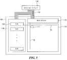
- FIG. 5 is a schematic view illustrating a display device according to an embodiment of the present invention.
- FIG. 6 is an equivalent circuit diagram illustrating compensation signals and elements in a pixel region according to a first embodiment of the present invention
- FIG. 7 is an equivalent circuit diagram of a shift register according to a first embodiment of the present invention.
- FIG. 8 is a graph showing an output signal of a shift register according to a first embodiment of the present invention.
- FIG. 9 is an equivalent circuit diagram showing compensation signals and elements in a pixel region according to a second embodiment of the present invention.
- FIG. 5 is a schematic view illustrating a display device according to an embodiment of the present invention.
- a gate line “GL” and a data line “DL” are formed on a substrate 100 .
- the gate line “GL” crosses the data line “DL” to define a pixel region 111 .
- the gate line “GL,” the data line “DL” and the pixel region 111 are disposed in a display region 110 of the substrate 100 .
- a gate driver 130 and a data driver 120 are formed at a periphery of the display region 110 .
- the data driver 120 applies an image signal to the data line “DL” and the gate driver 130 includes a plurality of shift registers 132 that apply a gate driving signal to the gate line “GL.”
- An external circuit 140 is connected to the data driver 120 and the gate driver 130 to supply the image signal, the gate driving signal and timing signals.
- the external circuit 140 may be formed as a printed circuit board (PCB).
- a thin film transistor including a gate electrode, a source electrode and a drain electrode and a storage capacitor may be formed in the pixel region 111 .
- the data line “DL” may be connected to the source electrode and the gate line “GL” may be connected to the gate electrode.
- the drain electrode may be connected to the storage capacitor.
- the substrate 100 may be used for a liquid crystal display (LCD) device and an organic electroluminescent display (OELD) device.
- the drain electrode may be connected to a liquid crystal capacitor.
- the drain electrode may be connected to another TFT that is connected to an organic electroluminescent diode.
- the TFT may be a P-type.
- the external circuit 140 may be connected to the substrate 100 using a tape carrier package (TCP) or a flexible printed circuit board (FPC: flexible PCB) 150 .
- TCP tape carrier package
- FPC flexible printed circuit board
- an integrated circuit (IC) for the external circuit 140 may be formed on a printed circuit board (PCB) and the PCB may be connected to the substrate 100 through a FPC.
- an IC for the external circuit 140 may be connected to the substrate 100 using an automated bonding (TAB) method.
- TFT automated bonding
- the external circuit 140 may supply various voltage signals to the TFT in the pixel region 111 to improve its characteristics. For example, a stabilization process of a P-type pixel TFT may be performed by applying an OFF-state offset.
- FIG. 6 is an equivalent circuit diagram showing signals and elements in a pixel region according to a first embodiment of the present invention.
- the external circuit supplies an AC (alternating current) voltage to a storage capacitor “C ST ” through a common line “CL.”
- the common line “CL” may be connected to a common electrode of a liquid crystal capacitor “C LC ” and the AC voltage may be applied through the common electrode. Accordingly, an OFF-state offset is applied to the P-type TFT “SW.”
- the positive voltage may be supplied from a shift register 132 (of FIG. 5 ) connected to the gate line “GL.”
- An output signal of the shift register may be adjusted by compensation signals of the external circuit.
- FIG. 7 is an equivalent circuit diagram of a shift register according to a first embodiment of the present invention
- FIG. 8 is a graph showing an output signal of a shift register according to a first embodiment of the present invention.
- the graph of FIG. 8 is obtained by a P-SPICE simulation.
- a plurality of clocks and a vertical start signal “VSTA” may be input to a shift register.
- a clock having a maximum value of about +10V and a minimum value of about ⁇ 8V may be input to the shift register as the vertical start signal “VSTA” and a gate driving pulse may be output from the shift register.
- a positive voltage is required to be applied to a gate line “GL” (of FIG. 6 ) and the shift register may output the positive voltage by inputting a DC (direct current) voltage instead of the clock.
- the DC voltage having one of about +10V and ⁇ 8V may be input to the shift register from the external circuit having an additional switch (not shown).
- a positive voltage of about 10V is output from the shift register when the DC voltage is input to the shift register.
- FIG. 9 is an equivalent circuit diagram showing signals and elements in a pixel region according to a second embodiment of the present invention.
- an external circuit 140 supplies an AC (alternating current) voltage to a data line “DL” and a positive voltage to a gate line “GL.”
- the external circuit may supply a DC (direct current) voltage to a storage capacitor “C ST ” through a common line “CL.”
- the common line “CL” may be connected to a common electrode of a liquid crystal capacitor “C LC ” and the DC voltage may be applied through the common electrode. Accordingly, an OFF-state offset is applied to the P-type TFT “SW.”
- an OFF-state offset is applied to a P-type TFT using an external circuit connected to a display panel, an additional process for stabilization of the P-type TFT is not required.
- the OFF-state offset is applied after forming the external circuit in a TAB method using TCP or FPC, or after connecting the external circuit on a PCB with the display panel. Accordingly, a stabilization process for a P-type TFT may be performed without increasing the total processing steps.
- an additional pad is not formed on a display panel, a static electricity, due to the pad, is prevented.
- the stabilization process for a P-type TFT may be applied to a liquid crystal display (LCD) device or an organic electroluminescent display (OELD) device.
- LCD liquid crystal display
- OELD organic electroluminescent display
Abstract
Description
Claims (7)
Priority Applications (1)
| Application Number | Priority Date | Filing Date | Title |
|---|---|---|---|
| US12/385,795 US8436796B2 (en) | 2003-06-23 | 2009-04-20 | Method of reducing off-current of a thin film transistor for display device and circuit for the same |
Applications Claiming Priority (2)
| Application Number | Priority Date | Filing Date | Title |
|---|---|---|---|
| KR10-2003-0040752A KR100531246B1 (en) | 2003-06-23 | 2003-06-23 | FPD and the bias aging method for PMOS device |
| KRP2003-0040752 | 2003-06-23 |
Related Child Applications (1)
| Application Number | Title | Priority Date | Filing Date |
|---|---|---|---|
| US12/385,795 Division US8436796B2 (en) | 2003-06-23 | 2009-04-20 | Method of reducing off-current of a thin film transistor for display device and circuit for the same |
Publications (2)
| Publication Number | Publication Date |
|---|---|
| US20040257147A1 US20040257147A1 (en) | 2004-12-23 |
| US7522139B2 true US7522139B2 (en) | 2009-04-21 |
Family
ID=33516446
Family Applications (2)
| Application Number | Title | Priority Date | Filing Date |
|---|---|---|---|
| US10/865,798 Active 2026-05-23 US7522139B2 (en) | 2003-06-23 | 2004-06-14 | Method of reducing OFF-current of a thin film transistor for display device and circuit for the same |
| US12/385,795 Active 2025-10-30 US8436796B2 (en) | 2003-06-23 | 2009-04-20 | Method of reducing off-current of a thin film transistor for display device and circuit for the same |
Family Applications After (1)
| Application Number | Title | Priority Date | Filing Date |
|---|---|---|---|
| US12/385,795 Active 2025-10-30 US8436796B2 (en) | 2003-06-23 | 2009-04-20 | Method of reducing off-current of a thin film transistor for display device and circuit for the same |
Country Status (2)
| Country | Link |
|---|---|
| US (2) | US7522139B2 (en) |
| KR (1) | KR100531246B1 (en) |
Cited By (2)
| Publication number | Priority date | Publication date | Assignee | Title |
|---|---|---|---|---|
| US20070216299A1 (en) * | 2006-03-20 | 2007-09-20 | Samsung Electronics Co., Ltd., | Display device and method of manufacturing the same |
| CN108417143A (en) * | 2018-01-19 | 2018-08-17 | 云谷(固安)科技有限公司 | A kind of array substrate and display screen |
Families Citing this family (11)
| Publication number | Priority date | Publication date | Assignee | Title |
|---|---|---|---|---|
| KR100479770B1 (en) * | 2002-08-29 | 2005-04-06 | 엘지.필립스 엘시디 주식회사 | method and system for the reduction of off-current in Field Effect Transistor using off-stress |
| KR100531246B1 (en) * | 2003-06-23 | 2005-11-28 | 엘지.필립스 엘시디 주식회사 | FPD and the bias aging method for PMOS device |
| KR100714003B1 (en) * | 2005-08-22 | 2007-05-04 | 삼성에스디아이 주식회사 | shift resister circuit |
| KR101186878B1 (en) * | 2005-08-26 | 2012-10-02 | 엘지디스플레이 주식회사 | VA mode LCD and driving method thereof |
| KR100713227B1 (en) * | 2006-06-30 | 2007-05-02 | 삼성전자주식회사 | Display device and manufacturing method thereof |
| KR100805599B1 (en) * | 2007-03-16 | 2008-02-20 | 삼성에스디아이 주식회사 | Organic elcetroluminescence display and making method teherof |
| KR101127590B1 (en) * | 2010-03-29 | 2012-03-23 | 삼성모바일디스플레이주식회사 | Active Level Shift Driver Circuit, Liquid Crystal Display Device comprising ALS Driver and Driving method of Liquid Crystal Display Device |
| US9041453B2 (en) | 2013-04-04 | 2015-05-26 | Semiconductor Energy Laboratory Co., Ltd. | Pulse generation circuit and semiconductor device |
| CN103295530A (en) * | 2013-06-28 | 2013-09-11 | 深圳市华星光电技术有限公司 | Display panel with static protection function and electronic device |
| US9214127B2 (en) | 2013-07-09 | 2015-12-15 | Apple Inc. | Liquid crystal display using depletion-mode transistors |
| CN104157260B (en) * | 2014-09-10 | 2016-09-28 | 深圳市华星光电技术有限公司 | Gate driver circuit based on IGZO processing procedure |
Citations (9)
| Publication number | Priority date | Publication date | Assignee | Title |
|---|---|---|---|---|
| US4316101A (en) * | 1978-11-30 | 1982-02-16 | Licentia-Patent-Verwaltungs-G.M.B.H. | Circuit for switching and transmitting alternating voltages |
| US5945866A (en) * | 1996-02-27 | 1999-08-31 | The Penn State Research Foundation | Method and system for the reduction of off-state current in field effect transistors |
| US6169532B1 (en) * | 1997-02-03 | 2001-01-02 | Casio Computer Co., Ltd. | Display apparatus and method for driving the display apparatus |
| KR20020051513A (en) | 2000-12-22 | 2002-06-29 | 이구택 | Apparatus and method for automatically controlling input and output of anode cell in electro-plating |
| US6690149B2 (en) * | 2001-09-12 | 2004-02-10 | Sharp Kabushiki Kaisha | Power supply and display apparatus including thereof |
| US20040041618A1 (en) * | 2002-08-29 | 2004-03-04 | Lg.Philips Lcd Co., Ltd | Method and system for reduction of off-current in field effect transistors |
| US20040257147A1 (en) * | 2003-06-23 | 2004-12-23 | Hun Jeoung | Method of reducing OFF-current of a thin film transistor for display device and circuit for the same |
| US20050057580A1 (en) * | 2001-09-25 | 2005-03-17 | Atsuhiro Yamano | El display panel and el display apparatus comprising it |
| US7071932B2 (en) * | 2001-11-20 | 2006-07-04 | Toppoly Optoelectronics Corporation | Data voltage current drive amoled pixel circuit |
Family Cites Families (6)
| Publication number | Priority date | Publication date | Assignee | Title |
|---|---|---|---|---|
| US5248963A (en) * | 1987-12-25 | 1993-09-28 | Hosiden Electronics Co., Ltd. | Method and circuit for erasing a liquid crystal display |
| WO2000003349A1 (en) * | 1998-07-08 | 2000-01-20 | E Ink Corporation | Method and apparatus for sensing the state of an electrophoretic display |
| WO2001053882A1 (en) * | 2000-01-21 | 2001-07-26 | Citizen Watch Co., Ltd. | Driving method of liquid crystal display panel and liquid crystal display device |
| TWI238375B (en) * | 2000-05-31 | 2005-08-21 | Toshiba Corp | Pumping circuit and flat panel display device |
| JP4111785B2 (en) * | 2001-09-18 | 2008-07-02 | シャープ株式会社 | Liquid crystal display |
| KR20050004203A (en) * | 2002-05-24 | 2005-01-12 | 코닌클리케 필립스 일렉트로닉스 엔.브이. | An electrophoretic display and a method of driving an electrophoretic display |
-
2003
- 2003-06-23 KR KR10-2003-0040752A patent/KR100531246B1/en active IP Right Grant
-
2004
- 2004-06-14 US US10/865,798 patent/US7522139B2/en active Active
-
2009
- 2009-04-20 US US12/385,795 patent/US8436796B2/en active Active
Patent Citations (9)
| Publication number | Priority date | Publication date | Assignee | Title |
|---|---|---|---|---|
| US4316101A (en) * | 1978-11-30 | 1982-02-16 | Licentia-Patent-Verwaltungs-G.M.B.H. | Circuit for switching and transmitting alternating voltages |
| US5945866A (en) * | 1996-02-27 | 1999-08-31 | The Penn State Research Foundation | Method and system for the reduction of off-state current in field effect transistors |
| US6169532B1 (en) * | 1997-02-03 | 2001-01-02 | Casio Computer Co., Ltd. | Display apparatus and method for driving the display apparatus |
| KR20020051513A (en) | 2000-12-22 | 2002-06-29 | 이구택 | Apparatus and method for automatically controlling input and output of anode cell in electro-plating |
| US6690149B2 (en) * | 2001-09-12 | 2004-02-10 | Sharp Kabushiki Kaisha | Power supply and display apparatus including thereof |
| US20050057580A1 (en) * | 2001-09-25 | 2005-03-17 | Atsuhiro Yamano | El display panel and el display apparatus comprising it |
| US7071932B2 (en) * | 2001-11-20 | 2006-07-04 | Toppoly Optoelectronics Corporation | Data voltage current drive amoled pixel circuit |
| US20040041618A1 (en) * | 2002-08-29 | 2004-03-04 | Lg.Philips Lcd Co., Ltd | Method and system for reduction of off-current in field effect transistors |
| US20040257147A1 (en) * | 2003-06-23 | 2004-12-23 | Hun Jeoung | Method of reducing OFF-current of a thin film transistor for display device and circuit for the same |
Non-Patent Citations (1)
| Title |
|---|
| Communication from Korean Patent Office. |
Cited By (2)
| Publication number | Priority date | Publication date | Assignee | Title |
|---|---|---|---|---|
| US20070216299A1 (en) * | 2006-03-20 | 2007-09-20 | Samsung Electronics Co., Ltd., | Display device and method of manufacturing the same |
| CN108417143A (en) * | 2018-01-19 | 2018-08-17 | 云谷(固安)科技有限公司 | A kind of array substrate and display screen |
Also Published As
| Publication number | Publication date |
|---|---|
| US20040257147A1 (en) | 2004-12-23 |
| US20090267929A1 (en) | 2009-10-29 |
| US8436796B2 (en) | 2013-05-07 |
| KR20050000162A (en) | 2005-01-03 |
| KR100531246B1 (en) | 2005-11-28 |
Similar Documents
| Publication | Publication Date | Title |
|---|---|---|
| US8436796B2 (en) | Method of reducing off-current of a thin film transistor for display device and circuit for the same | |
| US9898985B2 (en) | Gate on array drive system of raising yield and liquid crystal panel having the same | |
| US7733312B2 (en) | Liquid crystal display with a structure for reducing corrosion of display signal lines | |
| US8723853B2 (en) | Driving device, display apparatus having the same and method of driving the display apparatus | |
| US8218121B2 (en) | Liquid crystal display having a printed circuit board combined with only one of the tape carrier packages | |
| US9076394B2 (en) | Active matrix substrate, liquid crystal panel, liquid crystal display device, television receiver | |
| KR101006438B1 (en) | Liquid crystal display | |
| US9633615B2 (en) | Liquid crystal display device | |
| KR20110107659A (en) | Liquid crystal display | |
| KR101046927B1 (en) | Thin film transistor array panel | |
| US7123230B2 (en) | System and method for reducing off-current in thin film transistor of liquid crystal display device | |
| KR100898791B1 (en) | Method and Apparatus for Driving Liquid Crystal Display | |
| US20130162508A1 (en) | Driving Circuit of a Liquid Crystal Panel and an LCD | |
| US11823636B2 (en) | Array substrate, display device and driving method thereof | |
| US8704746B2 (en) | Liquid crystal display having a voltage stabilization circuit and driving method thereof | |
| US20130100005A1 (en) | LCD Panel and Method of Manufacturing the Same | |
| US7038644B2 (en) | Apparatus for applying OFF-state stress to P-MOS device | |
| KR100914782B1 (en) | Substrate of thin film transistor and liquid crystal display using the same | |
| EP1909256B1 (en) | Liquid crystal display and driving method therefor | |
| KR101712204B1 (en) | Display device and fabricating method thereof | |
| KR100922794B1 (en) | Liquid Crystal Display Device | |
| KR100923350B1 (en) | Liquid Crystal Display and Driving Method thereof | |
| KR20050040618A (en) | Liquid crystal display device and driving method thereof | |
| KR20060018395A (en) | Liquid crystal display | |
| BENCHIKH et al. | Structure Operating and Manufacturing of AMLCD Devices |
Legal Events
| Date | Code | Title | Description |
|---|---|---|---|
| AS | Assignment |
Owner name: L.G. PHILIPS LCD CO., LTD, STATELESS Free format text: ASSIGNMENT OF ASSIGNORS INTEREST;ASSIGNORS:JEOUNG, HUN;LEE, SUNG-HAK;REEL/FRAME:016136/0908 Effective date: 20040524 |
|
| AS | Assignment |
Owner name: LG DISPLAY CO., LTD., KOREA, REPUBLIC OF Free format text: CHANGE OF NAME;ASSIGNOR:LG.PHILIPS LCD CO., LTD.;REEL/FRAME:021763/0177 Effective date: 20080304 Owner name: LG DISPLAY CO., LTD.,KOREA, REPUBLIC OF Free format text: CHANGE OF NAME;ASSIGNOR:LG.PHILIPS LCD CO., LTD.;REEL/FRAME:021763/0177 Effective date: 20080304 |
|
| FEPP | Fee payment procedure |
Free format text: PAYER NUMBER DE-ASSIGNED (ORIGINAL EVENT CODE: RMPN); ENTITY STATUS OF PATENT OWNER: LARGE ENTITY Free format text: PAYOR NUMBER ASSIGNED (ORIGINAL EVENT CODE: ASPN); ENTITY STATUS OF PATENT OWNER: LARGE ENTITY |
|
| STCF | Information on status: patent grant |
Free format text: PATENTED CASE |
|
| FEPP | Fee payment procedure |
Free format text: PAYER NUMBER DE-ASSIGNED (ORIGINAL EVENT CODE: RMPN); ENTITY STATUS OF PATENT OWNER: LARGE ENTITY Free format text: PAYOR NUMBER ASSIGNED (ORIGINAL EVENT CODE: ASPN); ENTITY STATUS OF PATENT OWNER: LARGE ENTITY |
|
| FPAY | Fee payment |
Year of fee payment: 4 |
|
| FPAY | Fee payment |
Year of fee payment: 8 |
|
| MAFP | Maintenance fee payment |
Free format text: PAYMENT OF MAINTENANCE FEE, 12TH YEAR, LARGE ENTITY (ORIGINAL EVENT CODE: M1553); ENTITY STATUS OF PATENT OWNER: LARGE ENTITY Year of fee payment: 12 |