US7508570B1 - Gray level method for slim-based optical lithography - Google Patents
Gray level method for slim-based optical lithography Download PDFInfo
- Publication number
- US7508570B1 US7508570B1 US11/923,390 US92339007A US7508570B1 US 7508570 B1 US7508570 B1 US 7508570B1 US 92339007 A US92339007 A US 92339007A US 7508570 B1 US7508570 B1 US 7508570B1
- Authority
- US
- United States
- Prior art keywords
- substrate
- spatial light
- light modulator
- slm
- photosensitive coating
- Prior art date
- Legal status (The legal status is an assumption and is not a legal conclusion. Google has not performed a legal analysis and makes no representation as to the accuracy of the status listed.)
- Expired - Lifetime
Links
- 238000000034 method Methods 0.000 title claims description 59
- 238000000206 photolithography Methods 0.000 title abstract description 33
- 239000000758 substrate Substances 0.000 claims abstract description 297
- 239000011248 coating agent Substances 0.000 claims description 32
- 238000000576 coating method Methods 0.000 claims description 32
- 238000005286 illumination Methods 0.000 claims description 31
- 238000013461 design Methods 0.000 claims description 9
- 230000004075 alteration Effects 0.000 claims description 4
- 238000003384 imaging method Methods 0.000 abstract description 18
- 238000003491 array Methods 0.000 description 80
- 238000009826 distribution Methods 0.000 description 34
- 230000007246 mechanism Effects 0.000 description 27
- 238000006073 displacement reaction Methods 0.000 description 20
- 238000001459 lithography Methods 0.000 description 17
- 230000008569 process Effects 0.000 description 16
- 230000006837 decompression Effects 0.000 description 13
- 239000003550 marker Substances 0.000 description 13
- 230000003287 optical effect Effects 0.000 description 13
- 230000000694 effects Effects 0.000 description 8
- WYTGDNHDOZPMIW-RCBQFDQVSA-N alstonine Natural products C1=CC2=C3C=CC=CC3=NC2=C2N1C[C@H]1[C@H](C)OC=C(C(=O)OC)[C@H]1C2 WYTGDNHDOZPMIW-RCBQFDQVSA-N 0.000 description 7
- 238000010586 diagram Methods 0.000 description 6
- 238000000059 patterning Methods 0.000 description 6
- 239000004642 Polyimide Substances 0.000 description 4
- 238000013459 approach Methods 0.000 description 4
- 239000000463 material Substances 0.000 description 4
- 229920002120 photoresistant polymer Polymers 0.000 description 4
- 229920001721 polyimide Polymers 0.000 description 4
- 238000002360 preparation method Methods 0.000 description 4
- 239000004065 semiconductor Substances 0.000 description 4
- 230000008859 change Effects 0.000 description 3
- 238000001514 detection method Methods 0.000 description 3
- QSHDDOUJBYECFT-UHFFFAOYSA-N mercury Chemical compound [Hg] QSHDDOUJBYECFT-UHFFFAOYSA-N 0.000 description 3
- 229910052753 mercury Inorganic materials 0.000 description 3
- 238000012545 processing Methods 0.000 description 3
- 230000002441 reversible effect Effects 0.000 description 3
- 238000011960 computer-aided design Methods 0.000 description 2
- 238000013500 data storage Methods 0.000 description 2
- 230000007423 decrease Effects 0.000 description 2
- 238000011161 development Methods 0.000 description 2
- 230000006870 function Effects 0.000 description 2
- 230000000670 limiting effect Effects 0.000 description 2
- 238000004519 manufacturing process Methods 0.000 description 2
- 238000000926 separation method Methods 0.000 description 2
- 230000003068 static effect Effects 0.000 description 2
- XUIMIQQOPSSXEZ-UHFFFAOYSA-N Silicon Chemical compound [Si] XUIMIQQOPSSXEZ-UHFFFAOYSA-N 0.000 description 1
- 239000000654 additive Substances 0.000 description 1
- 230000000996 additive effect Effects 0.000 description 1
- 230000002238 attenuated effect Effects 0.000 description 1
- 230000008901 benefit Effects 0.000 description 1
- 238000004364 calculation method Methods 0.000 description 1
- 230000003247 decreasing effect Effects 0.000 description 1
- 238000010348 incorporation Methods 0.000 description 1
- 239000004973 liquid crystal related substance Substances 0.000 description 1
- 230000036961 partial effect Effects 0.000 description 1
- 230000008707 rearrangement Effects 0.000 description 1
- 229910052710 silicon Inorganic materials 0.000 description 1
- 239000010703 silicon Substances 0.000 description 1
- 239000007787 solid Substances 0.000 description 1
- 230000003595 spectral effect Effects 0.000 description 1
- 230000036962 time dependent Effects 0.000 description 1
- 235000012431 wafers Nutrition 0.000 description 1
- 238000003079 width control Methods 0.000 description 1
- 229910052724 xenon Inorganic materials 0.000 description 1
- FHNFHKCVQCLJFQ-UHFFFAOYSA-N xenon atom Chemical compound [Xe] FHNFHKCVQCLJFQ-UHFFFAOYSA-N 0.000 description 1
Images


Classifications
-
- G—PHYSICS
- G03—PHOTOGRAPHY; CINEMATOGRAPHY; ANALOGOUS TECHNIQUES USING WAVES OTHER THAN OPTICAL WAVES; ELECTROGRAPHY; HOLOGRAPHY
- G03F—PHOTOMECHANICAL PRODUCTION OF TEXTURED OR PATTERNED SURFACES, e.g. FOR PRINTING, FOR PROCESSING OF SEMICONDUCTOR DEVICES; MATERIALS THEREFOR; ORIGINALS THEREFOR; APPARATUS SPECIALLY ADAPTED THEREFOR
- G03F7/00—Photomechanical, e.g. photolithographic, production of textured or patterned surfaces, e.g. printing surfaces; Materials therefor, e.g. comprising photoresists; Apparatus specially adapted therefor
- G03F7/70—Microphotolithographic exposure; Apparatus therefor
- G03F7/70383—Direct write, i.e. pattern is written directly without the use of a mask by one or multiple beams
-
- G—PHYSICS
- G03—PHOTOGRAPHY; CINEMATOGRAPHY; ANALOGOUS TECHNIQUES USING WAVES OTHER THAN OPTICAL WAVES; ELECTROGRAPHY; HOLOGRAPHY
- G03F—PHOTOMECHANICAL PRODUCTION OF TEXTURED OR PATTERNED SURFACES, e.g. FOR PRINTING, FOR PROCESSING OF SEMICONDUCTOR DEVICES; MATERIALS THEREFOR; ORIGINALS THEREFOR; APPARATUS SPECIALLY ADAPTED THEREFOR
- G03F7/00—Photomechanical, e.g. photolithographic, production of textured or patterned surfaces, e.g. printing surfaces; Materials therefor, e.g. comprising photoresists; Apparatus specially adapted therefor
- G03F7/20—Exposure; Apparatus therefor
- G03F7/2022—Multi-step exposure, e.g. hybrid; backside exposure; blanket exposure, e.g. for image reversal; edge exposure, e.g. for edge bead removal; corrective exposure
- G03F7/2024—Multi-step exposure, e.g. hybrid; backside exposure; blanket exposure, e.g. for image reversal; edge exposure, e.g. for edge bead removal; corrective exposure of the already developed image
-
- G—PHYSICS
- G03—PHOTOGRAPHY; CINEMATOGRAPHY; ANALOGOUS TECHNIQUES USING WAVES OTHER THAN OPTICAL WAVES; ELECTROGRAPHY; HOLOGRAPHY
- G03F—PHOTOMECHANICAL PRODUCTION OF TEXTURED OR PATTERNED SURFACES, e.g. FOR PRINTING, FOR PROCESSING OF SEMICONDUCTOR DEVICES; MATERIALS THEREFOR; ORIGINALS THEREFOR; APPARATUS SPECIALLY ADAPTED THEREFOR
- G03F7/00—Photomechanical, e.g. photolithographic, production of textured or patterned surfaces, e.g. printing surfaces; Materials therefor, e.g. comprising photoresists; Apparatus specially adapted therefor
- G03F7/70—Microphotolithographic exposure; Apparatus therefor
- G03F7/70216—Mask projection systems
- G03F7/70275—Multiple projection paths, e.g. array of projection systems, microlens projection systems or tandem projection systems
-
- G—PHYSICS
- G03—PHOTOGRAPHY; CINEMATOGRAPHY; ANALOGOUS TECHNIQUES USING WAVES OTHER THAN OPTICAL WAVES; ELECTROGRAPHY; HOLOGRAPHY
- G03F—PHOTOMECHANICAL PRODUCTION OF TEXTURED OR PATTERNED SURFACES, e.g. FOR PRINTING, FOR PROCESSING OF SEMICONDUCTOR DEVICES; MATERIALS THEREFOR; ORIGINALS THEREFOR; APPARATUS SPECIALLY ADAPTED THEREFOR
- G03F7/00—Photomechanical, e.g. photolithographic, production of textured or patterned surfaces, e.g. printing surfaces; Materials therefor, e.g. comprising photoresists; Apparatus specially adapted therefor
- G03F7/70—Microphotolithographic exposure; Apparatus therefor
- G03F7/70216—Mask projection systems
- G03F7/70283—Mask effects on the imaging process
- G03F7/70291—Addressable masks, e.g. spatial light modulators [SLMs], digital micro-mirror devices [DMDs] or liquid crystal display [LCD] patterning devices
-
- G—PHYSICS
- G03—PHOTOGRAPHY; CINEMATOGRAPHY; ANALOGOUS TECHNIQUES USING WAVES OTHER THAN OPTICAL WAVES; ELECTROGRAPHY; HOLOGRAPHY
- G03F—PHOTOMECHANICAL PRODUCTION OF TEXTURED OR PATTERNED SURFACES, e.g. FOR PRINTING, FOR PROCESSING OF SEMICONDUCTOR DEVICES; MATERIALS THEREFOR; ORIGINALS THEREFOR; APPARATUS SPECIALLY ADAPTED THEREFOR
- G03F7/00—Photomechanical, e.g. photolithographic, production of textured or patterned surfaces, e.g. printing surfaces; Materials therefor, e.g. comprising photoresists; Apparatus specially adapted therefor
- G03F7/70—Microphotolithographic exposure; Apparatus therefor
- G03F7/70425—Imaging strategies, e.g. for increasing throughput or resolution, printing product fields larger than the image field or compensating lithography- or non-lithography errors, e.g. proximity correction, mix-and-match, stitching or double patterning
- G03F7/70466—Multiple exposures, e.g. combination of fine and coarse exposures, double patterning or multiple exposures for printing a single feature
-
- G—PHYSICS
- G03—PHOTOGRAPHY; CINEMATOGRAPHY; ANALOGOUS TECHNIQUES USING WAVES OTHER THAN OPTICAL WAVES; ELECTROGRAPHY; HOLOGRAPHY
- G03F—PHOTOMECHANICAL PRODUCTION OF TEXTURED OR PATTERNED SURFACES, e.g. FOR PRINTING, FOR PROCESSING OF SEMICONDUCTOR DEVICES; MATERIALS THEREFOR; ORIGINALS THEREFOR; APPARATUS SPECIALLY ADAPTED THEREFOR
- G03F7/00—Photomechanical, e.g. photolithographic, production of textured or patterned surfaces, e.g. printing surfaces; Materials therefor, e.g. comprising photoresists; Apparatus specially adapted therefor
- G03F7/70—Microphotolithographic exposure; Apparatus therefor
- G03F7/70483—Information management; Active and passive control; Testing; Wafer monitoring, e.g. pattern monitoring
- G03F7/70491—Information management, e.g. software; Active and passive control, e.g. details of controlling exposure processes or exposure tool monitoring processes
- G03F7/70508—Data handling in all parts of the microlithographic apparatus, e.g. handling pattern data for addressable masks or data transfer to or from different components within the exposure apparatus
-
- G—PHYSICS
- G03—PHOTOGRAPHY; CINEMATOGRAPHY; ANALOGOUS TECHNIQUES USING WAVES OTHER THAN OPTICAL WAVES; ELECTROGRAPHY; HOLOGRAPHY
- G03F—PHOTOMECHANICAL PRODUCTION OF TEXTURED OR PATTERNED SURFACES, e.g. FOR PRINTING, FOR PROCESSING OF SEMICONDUCTOR DEVICES; MATERIALS THEREFOR; ORIGINALS THEREFOR; APPARATUS SPECIALLY ADAPTED THEREFOR
- G03F7/00—Photomechanical, e.g. photolithographic, production of textured or patterned surfaces, e.g. printing surfaces; Materials therefor, e.g. comprising photoresists; Apparatus specially adapted therefor
- G03F7/70—Microphotolithographic exposure; Apparatus therefor
- G03F7/70483—Information management; Active and passive control; Testing; Wafer monitoring, e.g. pattern monitoring
- G03F7/7055—Exposure light control in all parts of the microlithographic apparatus, e.g. pulse length control or light interruption
- G03F7/70558—Dose control, i.e. achievement of a desired dose
-
- G—PHYSICS
- G03—PHOTOGRAPHY; CINEMATOGRAPHY; ANALOGOUS TECHNIQUES USING WAVES OTHER THAN OPTICAL WAVES; ELECTROGRAPHY; HOLOGRAPHY
- G03F—PHOTOMECHANICAL PRODUCTION OF TEXTURED OR PATTERNED SURFACES, e.g. FOR PRINTING, FOR PROCESSING OF SEMICONDUCTOR DEVICES; MATERIALS THEREFOR; ORIGINALS THEREFOR; APPARATUS SPECIALLY ADAPTED THEREFOR
- G03F7/00—Photomechanical, e.g. photolithographic, production of textured or patterned surfaces, e.g. printing surfaces; Materials therefor, e.g. comprising photoresists; Apparatus specially adapted therefor
- G03F7/70—Microphotolithographic exposure; Apparatus therefor
- G03F7/70691—Handling of masks or workpieces
- G03F7/70716—Stages
-
- H—ELECTRICITY
- H01—ELECTRIC ELEMENTS
- H01L—SEMICONDUCTOR DEVICES NOT COVERED BY CLASS H10
- H01L21/00—Processes or apparatus adapted for the manufacture or treatment of semiconductor or solid state devices or of parts thereof
- H01L21/02—Manufacture or treatment of semiconductor devices or of parts thereof
- H01L21/027—Making masks on semiconductor bodies for further photolithographic processing not provided for in group H01L21/18 or H01L21/34
- H01L21/0271—Making masks on semiconductor bodies for further photolithographic processing not provided for in group H01L21/18 or H01L21/34 comprising organic layers
- H01L21/0273—Making masks on semiconductor bodies for further photolithographic processing not provided for in group H01L21/18 or H01L21/34 comprising organic layers characterised by the treatment of photoresist layers
- H01L21/0274—Photolithographic processes
- H01L21/0275—Photolithographic processes using lasers
Definitions
- This invention relates to the field of optical lithography, and in particular to printing patterns on the following substrates: wafers; printed circuit boards; flat panel displays; masks; reticles; and plates used for the reproduction of magazines, newspapers and books.
- the semiconductor industry uses very expensive stepper tools for lithographic processing. Furthermore, very expensive reticles are used in this processing—the cost of the reticles is sufficient to make low volume production of chips (such as custom ASICs) prohibitively expensive.
- the semiconductor industry needs a lower cost lithography process. Furthermore, every time the lithography pattern changes, several days or more are required to produce a new reticle. The semiconductor industry needs a lithography process which can quickly accommodate pattern changes.
- PCB printed circuit board
- the printed circuit board (PCB) industry has similar problems with its lithography processes. Furthermore, the substrates used in the PCB industry undergo distortion during fabrication which limits the use of high resolution lithography processing to small area substrates and the use of steppers. A high resolution lithographic process is required for large PCB substrates in which the pattern can be quickly and economically adjusted to accommodate the distortions, where the distortions vary from one substrate to the next.
- U.S. Pat. Nos. 5,330,878 5,523,193 5,482,818 and 5,672,464 to Nelson describe a method and apparatus for patterning a substrate.
- the apparatus uses a spatial light modulator (SLM), specifically the Texas Instruments deformable mirror device (DMD), in place of a reticle.
- SLM spatial light modulator
- DMD Texas Instruments deformable mirror device
- An image of the DMD is projected on the substrate by an imaging lens. Whether or not an individual element of the DMD reflects light into the imaging lens, such that it is projected on the substrate, is determined by computer; thus the pattern projected on the substrate is computer controlled and readily changed. Improvements are required to this approach in order to meet the high resolution and throughput requirements of both the semiconductor and PCB industries. Furthermore, advancements are available to reduce the cost of the apparatus, while increasing the throughput and meeting the high resolution requirements.
- the present invention provides an apparatus and method for patterning photosensitive substrates.
- the apparatus includes a spatial light modulator (SLM), a light source for illuminating the SLM, imaging optics for projecting an image of the SLM on the substrate, and means for moving the image across the surface of the substrate.
- the SLM controls the pattern of light which reaches the substrate.
- the SLM comprises at least one array of individually switchable elements—switchable between two or more states.
- the SLM can be either a diffractive or a transmissive device.
- the light source can be a continuous light source, such as an arc lamp, LED or continuous laser; quasi-continuous lasers can also be used when the laser pulsing frequency is much higher than the switching frequency of the elements of the SLM.
- the means for moving the image can be a stage on which either the SLM or the substrate is mounted.
- the substrate When the substrate is in the form of a flexible film or similar, it may be moved using a reel to reel mechanism. While the image is moving across the surface of the substrate, elements of the spatial light modulator are switched such that a pixel on the surface of the substrate receives, in serial, doses of energy from multiple elements of the spatial light modulator, thus forming a latent image on the substrate surface.
- the imaging optics can be telecentric.
- the imaging optics is configured to project a blurred image of the spatial light modulator on the substrate, enabling sub-pixel resolution feature edge placement.
- the blurring can be implemented by: adjusting the focus of the imaging optics; adjusting the numerical aperture of the imaging optics; adding a diffuser between the SLM and the substrate; adding a microlens array between the SLM and the substrate; or a combination of the aforementioned.
- the spatial light modulator is continuously illuminated, an image of the spatial light modulator is continuously projected on the substrate, and the image is continuously moved across the surface of the substrate.
- the SLM comprises a multiplicity of area arrays.
- the corresponding imaging optics can be a single projection lens system, or a multiplicity of projection lens systems.
- the number of the area arrays is greater than the number of the projection lens systems, and the number of projection lens systems is preferably a submultiple of the number of area arrays.
- the multiplicity of area arrays can be arranged in a line, or they can be arranged in multiple lines where the placement of the arrays is staggered from one line to another. The latter may utilize more of the imaging field of the projection optics, and can also result in a more efficient exposure of the substrate—reducing the need for a serpentine motion of the projected image of the SLM across the substrate during exposure.
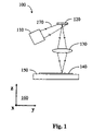
- FIG. 1 is a schematic representation of an optical lithography tool with a movable substrate, in accordance with the invention.
- FIG. 2 is a schematic representation of an optical lithography tool with a movable spatial light modulator, in accordance with the invention.
- FIG. 3 is a schematic representation of an optical lithography tool with a flexible film substrate, in accordance with the invention.
- FIG. 4 is a detailed schematic representation of a first embodiment of the optical lithography tool of FIG. 1 , showing telecentric projection optics.
- FIG. 5 is a detailed schematic representation of a second embodiment of the optical lithography tool of FIG. 1 , showing a spatial light modulator with multiple area arrays and corresponding multiple sets of projection optics.
- FIG. 6 is a detailed schematic representation of a third embodiment of the optical lithography tool of FIG. 1 , showing a spatial light modulator with multiple area arrays and a single set of telecentric projection optics.
- FIG. 7 is a diagrammatic cross-sectional view through part of a micro-mirror array in accordance with the invention, showing array elements in ‘on’ and ‘off’ positions.
- FIG. 8 is a plan view of a substrate showing a serpentine path that can be followed by the projected image of a spatial light modulator in order to expose the entire substrate surface, in accordance with the invention.
- FIG. 9 is a plan view of a substrate showing serpentine paths that can be followed by projected images from each of a multiplicity of area arrays that are used together to expose the entire substrate surface, in accordance with the invention.
- FIG. 10 is a diagrammatic representation of the process of forming a latent image, in accordance with the invention.
- FIG. 11 is a diagrammatic representation of the substrate array of FIG. 10 .
- FIG. 12 is a graph showing instantaneous light intensity distributions along the line segment AB on the substrate of FIG. 10 , at equally spaced time intervals T/10, starting at T 3 .
- FIG. 13 is a graph showing instantaneous light intensity distributions along the line segment AB on the substrate of FIG. 10 , at equally spaced time intervals T/10, ending at T 4 .
- FIG. 14 is a graph showing the integrated dose distribution along the line segment AB on the substrate of FIG. 10 , due to light exposure between times T 3 and T 4 .
- FIG. 15 is a graph showing the total dose distribution along the line segment AB on the substrate of FIG. 10 , due to light exposure between times T 1 and T 7 .
- FIG. 16 is a diagrammatic representation of the process of forming a latent image including a first example of edge shifting by one half of the projected width of a mirror, in accordance with the invention.
- FIG. 17 is a diagrammatic representation of the process of forming a latent image including a second example of edge shifting by one half of the projected width of a mirror, in accordance with the invention.
- FIG. 18 is a diagrammatic representation of the process of forming a latent image including an example of edge shifting by one quarter of the projected width of a mirror, in accordance with the invention.
- FIG. 19 is a diagrammatic representation of the process of forming a latent image including an example of edge shifting by three quarters of the projected width of a mirror, in accordance with the invention.
- FIG. 20 is a diagrammatic representation of the process of forming a latent image including an example of edge shifting in another direction by one quarter of the projected width of a mirror, in accordance with the invention.
- FIG. 21 is a graph showing the integrated dose distributions along the line segment AB on the substrates of FIGS. 10 , 16 , 17 , 18 and 19 .
- FIG. 22 is a further diagrammatic representation of the process of forming a latent image, in accordance with the invention.
- FIG. 23 is a diagrammatic representation of the substrate array of FIG. 22 .
- FIG. 24 is a graph showing the integrated dose distributions along the line segments CD, EF, GH and IJ on the substrate of FIG. 22 .
- FIG. 25 is a diagrammatic representation of the process of forming a latent image including a further example of edge shifting, in accordance with the invention.
- FIG. 26 is a diagrammatic representation of the substrate array of FIG. 25 .
- FIG. 27 is a graph showing the integrated dose distributions along the line segments KL, MN, OP, QR and ST on the substrate of FIG. 25 .
- FIG. 28 is a block diagram of an optical lithography system in accordance with the invention.
- FIG. 29 is a plan view of an arrangement of multiple area arrays in accordance with an embodiment of the invention.
- FIG. 30 is a schematic representation of another embodiment of the optical lithography tool of FIG. 4 , showing a light switching mechanism 121 on the light path between the light source and the substrate.
- FIG. 31 is a timing diagram of an optical lithography system with two spatial light modulators configured in serial on the light path, in accordance with the invention.
- FIG. 32 is a diagrammatic representation of the process of forming a latent image using an optical lithography system with two spatial light modulators configured in serial on the light path, in accordance with the invention.
- FIG. 33 is a timing diagram of an optical lithography system with a spatial light modulator and a light switching mechanism configured in serial on the light path, in accordance with the invention.
- FIG. 34 is a schematic representation of an optical lithography tool with light optics configured to overlap projected images of two area arrays on the substrate surface, in accordance with the invention.
- FIG. 35 is a timing diagram of the optical lithography system of FIG. 34 .
- optical lithography tool 100 which is an embodiment of the invention suitable for patterning a substrate 140 mounted on a movable stage 150 , is shown with a light source 110 , a spatial light modulator (SLM) 120 and imaging optics 130 .
- Coordinate axes 160 are shown with the z and y axes in the plane of the figure and the x axis perpendicular to the plane of the figure.
- the light path through the optical lithography tool is represented by rays 170 .
- the light source 110 continuously illuminates the SLM 120 .
- the light source may comprise an arc lamp, continuous laser (solid state or gas), light emitting diode (LED) or other type of continuous light source that has suitable spectral properties for exposure of the substrate 140 .
- a light source such as a quasi-continuous laser (a laser which is pulsed at MHz frequencies), may be suitable as a light source for this invention—a critical criteria is that the pulsing frequency be much higher than the switching frequency for elements of the spatial light modulator (typically 10 4 Hz); in this case the illumination of the SLM by the light source is effectively continuous.
- the light source may also comprise optical components for increasing the intensity of illumination and to improve illumination uniformity. These may include an elliptical mirror, both round and cylindrical lenses, and light pipes or fly's eye lens arrays.
- SLM 120 is one or more area arrays (generally rectangular) of elements that act on the light beam from the light source.
- An image of the SLM is continuously projected onto the substrate by the imaging optics 130 , which is also referred to as the projection optics.
- the elements can be individually switched between two or more states, under computer control, so as to control the light amplitude in the image.
- One embodiment of the invention includes an SLM which is an array of mirrors or diffractive elements that can switch incoming light rays between two or more angular states.
- a digital micro-mirror device (DMD), currently available from Texas Instruments, is an example of a suitable mirror-array that can switch between two angular states.
- a diffractive SLM is the Grating Light Valve (GLV) currently manufactured by Silicon Light Machines.
- SLMs which are Liquid Crystal Display (LCD) devices. If the elements of the SLM are transmissive, rather than reflective, then the optics will need to be rearranged; such a rearrangement will be obvious to those skilled in the art.
- Imaging lens system 130 may contain both reflective and refractive elements, and is typically telecentric.
- Substrate 140 either includes a photosensitive layer, such as a photoresist coating, or is itself a photosensitive material, such as a sheet of photosensitive polyimide.
- the stage 150 may be of a roller-bearing or air-bearing design and may have height adjustment (in z-direction), tilt and rotation capabilities. These types of stages are well know and commonly used in lithography systems. For simplicity of illustration the substrate is assumed to be planar. However, the invention will also work with other substrate shapes, such as cylindrical or spherical, along with a rotary rather than a planar stage.
- optical lithography tool 200 which is an embodiment of the invention suitable for patterning a static substrate 140 , is shown with a light source 110 , SLM 120 , a stage 250 on which the SLM is mounted, and projection optics 130 .
- the method of operation is the same as for optical lithography system 100 , described above, except that stage 250 moves SLM 120 during exposure while substrate 140 is stationary.
- Imaging lens system 130 and/or illumination source 110 can also be attached to the stage 250 and move with the SLM.
- optical lithography tool 300 which is an embodiment of the invention suitable for patterning a flexible substrate 340 , is shown with a light source 110 , SLM 120 , a stage 250 on which the SLM is mounted, projection optics 130 , and rotatable, spaced apart, axially parallel film drums 342 and 344 .
- the photosensitive flexible film substrate 340 is wrapped around and tensioned between film drums 342 and 344 such that the film can be moved in the y direction (referenced to stationary coordinate system 160 ).
- Two modes of exposure are possible. In the first mode, stage 250 moves the SLM at constant speed in the x direction while the substrate 340 is stationary.
- the film drums index the substrate forward in the y direction and the stage reverses direction for the next exposure pass.
- the result is a serpentine exposure path similar to path 850 shown in FIG. 8 , and discussed in more detail below.
- the film drums move the substrate at constant speed in the y direction until the edge of the exposure region is reached.
- the stage indexes the substrate forward in the x direction and the film drums reverse direction for the next exposure pass. Again, this results in a serpentine exposure path.
- the stage can remain stationary, or be eliminated, and the film drums move the substrate at a constant speed, without the need to reverse direction.
- the projection optics may be carried on the stage.
- FIGS. 4 , 5 and 6 different embodiments of optical lithography tool 100 (see FIG. 1 ) are shown in detail.
- FIG. 4 is a schematic of a continuous direct-write optical lithography system with an arc lamp and a telecentric projection lens system.
- Continuous illumination from mercury arc lamp 410 is reflected from elliptical reflector 411 .
- Reflected light as represented by light rays 170 , travels to a dichroic mirror 412 , which reflects wavelengths useful for exposure of the substrate 140 (for example 350 nm-450 nm) and is transparent to other wavelengths.
- Light not reflected from the dichroic mirror is absorbed in illumination beam dump 413 .
- Other types of lamps can be used, such as a Xenon arc lamp, depending on the exposure wavelengths and source brightness needed.
- a light pipe 415 is used to improve the illumination uniformity, but could be replaced with a fly's eye lens array.
- a light pipe lens system 414 positioned before the light pipe 415 , is used to adjust the numerical aperture of the illumination system and to adjust the diameter of the light beam prior to entering the light pipe.
- Condenser lens system 416 captures light exiting from the light pipe and modifies the beam shape and angle to match the requirements of the SLM 120 .
- the condenser lens system contains an illumination aperture 417 .
- the light pipe lens system and condenser lens system are usually anamorphic and contain cylindrical lens elements.
- the continuous illumination mercury arc lamp, elliptical reflector, dichroic mirror, illumination beam dump, light pipe lens system, light pipe, condenser lens system and illumination aperture comprise an embodiment of illumination source 110 , as shown in FIG. 1 .
- the SLM is one or more area arrays (generally rectangular) of small mirrors that can switch between two or more angular states under computer control. At least one of the angular states reflects light rays from the illumination source into a telecentric projection lens system 430 and at least one other angular state reflects light rays into an SLM beam dump 480 .
- a digital micro-mirror device (DMD), currently available from Texas Instruments, is an example of a suitable mirror-array that can switch between two angular states.
- the substrate either contains a photosensitive layer, such as a photoresist coating, or is itself a photosensitive material, such as a sheet of photosensitive polyimide.
- the substrate is attached to stage 150 , which moves continuously during exposure in straight-line segments in the x-y plane of stationary coordinate system 160 .
- the numerical aperture of the telecentric projection lens system is determined by a projection lens aperture 432 , which is optically conjugate to illumination aperture 417 .
- a double telecentric projection lens system is shown. However, a single telecentric or non-telecentric projection system will also work. A telecentric design is preferred because the magnification does not change with substrate height, which simplifies calibration of the lithography tool for each substrate.
- the telecentric projection lens system is a type of projection lens system 130 , as shown in FIG. 1 .
- the stage can move in a plane x-y and also in the z direction of the stationary coordinate system 160 .
- the stage 150 can also have rotation and tilt capability; this may be required for proper substrate alignment (for example, when substrate flatness is an issue). Movement in the z direction will either focus or defocus the projected image on the substrate.
- a substrate height measuring system 450 can be used to determine the z position of the surface of the substrate 140 .
- the height measuring system can be optical, capacitance or air based. The preferred type is air. Focusing can also be accomplished by moving either the SLM or projection lens system in the z direction.
- FIG. 5 is a schematic of a continuous direct-write optical lithography system with an arc lamp, an SLM with multiple area arrays, and multiple projection lens systems.
- the light source is arranged as described above for FIG. 4 , except that a condenser lens system 516 and lens array 518 capture light exiting from light pipe 415 , so as to modify the beam shape and angle to match the requirements of the individual SLM area arrays 520 through 524 .
- the lens array maximizes the light intensity on the individual SLM area arrays; the lens array is configured to match the arrangement of the SLM area arrays, which may be arranged in a line, multiple lines (see FIG. 29 ), or some other two dimensional arrangement. While not an essential component, incorporation of the lens array is preferred.
- the lens array may comprise lenses arranged correspondingly with the SLM area arrays; alternatively, the lenses in the lens array may be replaced with one or more diffractive elements.
- Light pipe lens system 414 and condenser lens system 516 are usually anamorphic and contain cylindrical lens elements.
- the continuous illumination mercury arc lamp 410 , elliptical reflector 411 , dichroic mirror 412 , illumination beam dump 413 , light pipe lens system 414 , light pipe 415 , condenser lens system 516 and lens array 518 comprise a type of continuous illumination source 110 as in FIG. 1 .
- Each individual SLM area array 520 through 524 is a rectangular array of small mirrors that can switch between two or more angular states under computer control.
- a digital micro-mirror device currently available from Texas Instruments is an example of a suitable mirror-array that can switch between two angular states.
- Mirrors in the “on” state in SLM area array 520 are imaged on the substrate 140 by projection lens 530 ; likewise for SLM area arrays 521 through 524 and their corresponding projection lenses 531 through 534 .
- Light reflected from mirrors in SLM area array 520 in the “off” state travels to SLM beam dump 480 where it is absorbed; likewise for SLM area arrays 521 through 524 .
- each SLM area arrays ( 520 through 524 ), projection lenses ( 530 through 534 ) and substrate height measuring systems ( 550 through 554 ) are shown in this example, but any number may be used.
- the projection lenses may contain both reflective and refractive elements, and are typically telecentric.
- the projection lens systems (any one of 530 through 534 ) may be the same as the projection optics 130 in FIG. 1 .
- Substrate 140 either contains a photosensitive layer, such as a photoresist coating, or is itself a photosensitive material, such as a sheet of photosensitive polyimide.
- the substrate is attached to stage 150 , which moves continuously during exposure in straight-line segments in the x-y plane of stationary coordinate system 160 .
- the imaging optics may be carried on the stage.
- FIG. 6 is a schematic of a continuous direct-write optical lithography system with a single telecentric objective lens system and a SLM with multiple area arrays.
- the light source 610 is the same as the light source described in FIG. 5 , and is configured so as to provide illumination to match the requirements of the individual SLM area arrays 520 through 524 .
- Each individual SLM area array is one or more rectangular arrays of small mirrors that can switch between two or more angular states under computer control.
- a digital micro-mirror device (DMD) currently available from Texas Instruments is an example of a suitable mirror-array that can switch between two angular states.
- DMD digital micro-mirror device
- Mirrors in the “on” state in the SLM area arrays are imaged on the substrate 140 by telecentric projection lens system 630 , Light reflected from mirrors in the SLM area arrays in the “off” state travels to SLM beam dump 480 where it is absorbed.
- Five SLM area arrays are shown in this example but any number may be used.
- a double telecentric projection lens system 630 is shown. However, a single telecentric or non-telecentric projection system can also be used.
- a telecentric design is preferred because the magnification does not change with substrate height, which simplifies calibration of the lithography tool for each substrate.
- the telecentric projection lens system is a type of projection lens system 130 , as in FIG. 1 .
- the stage can move in a plane x-y and also in the z direction of the stationary coordinate system 160 .
- the stage 150 can also have rotation and tilt capability; this may be required for proper substrate alignment (for example, when substrate flatness is an issue). Movement in the z direction will either focus or defocus the projected image on the substrate.
- a substrate height measuring system 450 can be used to determine the z position of the surface of the substrate 140 .
- the height measuring system can be optical, capacitance or air based. The preferred type is air. Focusing can also be accomplished by moving either the SLM area arrays 520 through 524 or telecentric projection lens system 630 in the z direction.
- Substrate 140 either contains a photosensitive layer, such as a photoresist coating, or is itself a photosensitive material, such as a sheet of photosensitive polyimide.
- a lithography system may have 6 SLM area arrays and 2 projection lens systems, such that each projection lens system images 3 different SLM area arrays at once.
- the number of projection lens systems need not be limited to a mathematical submultiple—for example, a lithography system may have 7 SLM area arrays and 2 projection lens systems, such that a first projection lens system images 3 SLM area arrays and a second projection lens system images the remaining 4 SLM area arrays.
- the configuration of these embodiments will be apparent to those skilled in the art.
- SLM area arrays and projection lens systems which follow this teaching and will be apparent to those skilled in the art.
- a partial cross-section of a SLM 720 is shown.
- Mirrors 721 are shown in the ‘on’ position and mirrors 722 are shown in the ‘off’ position.
- Light rays 770 are reflected off the surface of the mirrors 721 , which are in the ‘on’ position, toward a substrate (rays 771 ) and are reflected off the surface of mirrors 722 , which are in the ‘off’ position, toward a beam stop (rays 772 ).
- rays 771 travel through projection lens system 430 and then to the substrate 140
- the rays 772 fall outside the acceptance aperture of projection lens system 430 and are collected by beamstop 480 .
- the rays 772 could fall partly within the acceptance aperture of projection lens system 430 , consequently an attenuated signal from the “off” state mirrors would reach the substrate, which may be tolerable.
- FIG. 8 an example is shown of a serpentine path 850 that can be followed by the projected image of a SLM in order to expose the entire surface of the substrate 140 .
- the motion of the image is due to an image movement mechanism.
- the substrate or the SLM can be mounted on the image movement mechanism.
- An example of a suitable mechanism is a stage, such as shown in FIGS. 1 , 2 and 3 .
- a suitable mechanism is a pair of rotatable, spaced apart, axially parallel film drums, such as shown in FIG. 3 .
- FIG. 3 In the explanation that follows a configuration of the lithography system in which the substrate is mounted on a stage is assumed.
- substrate 140 serpentine path 850 , distance between straight line segments on the path 851 , substrate coordinate system 853 and stationary coordinate system 860 .
- the SLM is oriented in such a way that the columns of pixels in the projected image on the substrate are parallel to the straight-line segment portions of the serpentine path, which, for ease of illustration, are parallel to the x-axis of stationary coordinate system 860 .
- a stage positions the substrate 140 such that the center of the projected image of the SLM is at the beginning of path 850 . In this example, at the beginning of path 850 none of the projected image of the SLM falls on the substrate 140 .
- the center of the projected image of the SLM moves in the ⁇ x s direction, referenced to substrate coordinate system 853 , and traces the first straight section of the serpentine path.
- the exposure starts when the projected image of the SLM falls on the substrate.
- the exposure stops after the projected image clears the edge of the substrate.
- the stage then repositions the substrate in readiness to scan in the ⁇ x direction along the second straight section of the path, which is separated from the first straight section by a distance 851 in the y direction, all referenced to stationary coordinate system 860 . This is repeated until the entire substrate is exposed.
- the projected width of the SLM must be greater than or equal to the distance 851 in order to expose the complete substrate.
- serpentine path can also be achieved with a lithography system configuration in which the SLM is mounted on a stage and the substrate is static.
- FIG. 9 an example is shown of a set of serpentine paths 950 through 954 that can be followed by the projected images of a corresponding set of SLM area arrays in order to expose the entire surface of the substrate 140 .
- the motion of the image is due to an image movement mechanism.
- the substrate or the SLM can be mounted on the image movement mechanism.
- An example of a suitable mechanism is a stage, such as shown in FIGS. 1 , 2 and 3 .
- a suitable mechanism is a pair of rotatable, spaced apart, axially parallel film drums, such as shown in FIG. 3 .
- FIG. 3 In the explanation that follows a configuration of the lithography system in which the substrate is mounted on a stage is assumed.
- Each SLM area array is oriented in such a way that the columns of pixels in the projected image on the substrate 140 are parallel to the straight-line segment portions of the serpentine path, which for ease of illustration, are parallel to the x-axis of stationary coordinate system 860 .
- a stage positions the substrate 140 such that the centers of the projected images of the SLM area arrays are at the beginning of paths 950 through 954 . In this example, at the beginning of paths 950 through 954 none of the projected images of the SLM arrays fall on the substrate 140 .
- the stage moves in the +x direction, referenced to stationary coordinate system 860 , the center of the projected images of the SLM area arrays move in the ⁇ x s direction, referenced to substrate coordinate system 853 , and trace the first straight sections of the serpentine paths.
- the exposure along any path starts when the projected image of the SLM area array falls on the substrate.
- the stage then repositions the substrate in readiness to scan in the ⁇ x direction along the second straight section of the path, which is separated from the first straight section by a distance 851 in the y direction, all referenced to stationary coordinate system 860 .
- the stage moves in the y direction, referenced to stationary coordinate system 860 , by the distance between paths 950 and 954 , and the above procedure is repeated.
- the projected width of the SLM arrays must be greater than or equal to the distance 851 in order to expose the complete substrate. Note that in this example the separation between consecutive paths 950 , 951 , . . . 954 is twice the spacing 851 ; should the separation exceed twice the spacing 851 , then a serpentine motion with more straight sections can be employed. This explanation is relevant to the multiple SLM area array lithography systems of FIGS. 5 & 6 , for which paths 950 through 954 correspond to SLM area arrays 520 through 524 .
- patterns of elements in the “on” state that correspond to features printed on substrate 140 must shift across the SLM 120 in such a way that they appear stationary, on average, to the constantly moving substrate. If the stage 150 is moving at constant speed ⁇ along one of the straight-line segments of serpentine path 850 (the stage is moving in a patterning direction), then this is accomplished by shifting the SLM pattern by one row at regular time intervals, where the time interval T is given by:
- p is the row pitch of the elements (the Texas Instruments DMD mirrors have the same pitch for rows and columns) and M is the magnification of the projection lens system 130 .
- the Texas Instruments DMD is available with a mirror pitch of 13.7 microns and the minimum mirror cycle time is 102 microseconds. If the projection lens system 130 has a magnification of 2.0, then the stage speed is approximately 269 mm/s. If the dose delivered is inadequate to expose the substrate or the stage speed required is beyond the capability of the stage system, then the actual mirror cycle time used may need to be longer. However, the mirror cycle time and stage speed must always satisfy equation (1).
- FIG. 10 illustrates the shifting of patterns on the SLM and the corresponding image on the substrate.
- the substrate is on a stage and moves at constant speed in the x direction during exposures.
- part of SLM 120 which is an array of elements 1000 with an area of 4 rows by 6 columns
- a corresponding part of substrate 140 which is an array of pixels 1002 with an area of 4 rows by 6 columns
- resultant image 1007 with projected row pitch (width of a pixel) 1008 The resultant image shows one possible latent image on the substrate due to completion of the entire series of exposures. The edge placement and corner rounding in a latent image will be discussed in detail below.
- “Snapshots” of the corresponding parts of the SLM and substrate are shown at equally spaced times T 1 through T 7 , where the time interval satisfies equation (1); the parts of the SLM and substrate are indicated in the figure by M and S, respectively.
- the SLM array 1000 , the substrate array 1002 and the resultant image 1007 are drawn as if viewed from a position directly above them and looking down in the ⁇ z direction of stationary coordinate system 160 .
- the projected row pitch 1008 in the resultant image 1007 is the row pitch in the SLM array 1000 times the magnification of the projection lens system 130 .
- each “snapshot” the SLM and substrate arrays are shown having the same size and orientation.
- the grid shown on the arrays 1000 and 1002 , and the image 1007 is for reference only.
- a light square in 1000 corresponds to an SLM element in the “on” state, while a dark square corresponds to one in the “off” state.
- the light and dark areas in 1002 correspond to the states of the SLM elements for that “snapshot”.
- the substrate is receiving light at pixels located at R 1 C 4 and R 1 C 5 from mirrors in the SLM array at positions R 4 C 4 and R 4 C 5 (where the nomenclature R 1 C 4 represents the pixel/element at row R 1 and column C 4 ).
- the bottom edge of the substrate array 1002 is aligned with substrate position coordinate 1.
- the substrate has moved by one row and the bottom edge of the substrate is now aligned with substrate position coordinate 2.
- the time elapsed between T 2 and T 1 satisfies equation (1).
- the particular feature pattern used as an example in FIG. 10 is shown in its entirety at time T 4 on both the SLM and the substrate arrays. It can be seen that the edge of this feature pattern first appears at T 1 , scrolls across the SLM array 1000 between times T 2 and T 6 and has moved off the SLM array 1000 by T 7 . On the substrate array 1002 , the feature pattern does not appear to move. This can be most clearly seen at times T 3 and T 4 .
- the projected pattern does in fact move on the substrate by the projected row pitch 1008 between any two consecutive snapshot times. Note that for ease of illustration the patterns shown on the substrate arrays 1002 do not show any blurring or optical interference effects.
- FIG. 11 shows the substrate array 1002 with a line segment AB positioned in the center of column C 4 .
- Light intensity and resultant dose profiles will be determined on the surface of the substrate array in the position indicated by line segment AB. Note that the position of AB is such that it crosses the “trailing edge” of the exposure pattern shown in FIG. 10 .
- FIG. 12 shows instantaneous light intensity distributions on substrate array 1002 from FIG. 10 ; the distributions are along the position of line segment AB as shown in FIG. 11 . Note that in FIG. 12 the line segment AB is shown to extend from ⁇ 2 to 1.5 on the abscissa. In FIG. 12 , six distributions are shown at intervals of T/10 starting at T 3 and then every T/10, where T is defined in equation (1) above.
- the substrate is moving with constant velocity.
- the abscissa represents substrate displacement x s (as shown in FIGS. 8 and 9 ) measured in units of projected row pitch (as defined above in reference to FIG. 10 ). The following are shown in FIG.
- light intensity profiles 1200 , 1201 , 1202 , 1203 , 1204 and 1205 light intensity profiles 1200 , 1201 , 1202 , 1203 , 1204 and 1205 ; 50% light intensity marker 1209 ; 50% position marker 1210 ; and projected row pitch 1215 .
- the shape of light intensity profiles 1200 , 1201 , 1202 , 1203 , 1204 and 1205 is shown as being Gaussian; however, the actual shape depends on details of the optics.
- the instantaneous light intensity as a function of position on the substrate array 1002 at time T 3 is represented by light intensity profile 1200 .
- Light intensity profile 1200 is positioned such that the intersection of the 50% marker 1209 on the abscissa corresponds to the boundary between rows R 3 and R 4 on the substrate array.
- the region between ⁇ 1 and 0 on the abscissa corresponds to R 4 on the substrate array, the region between 0 and 1 corresponds to R 3 and the region between 1 and 2 corresponds to R 2 .
- the light intensity profiles 1201 , 1202 , 1203 , 1204 and 1205 are for times T 3 plus T/10, 2T/10, 3T/10, 4T/10 and 5T/10, respectively.
- the light intensity profile advances across the substrate in the ⁇ x s direction by one-half of the projected row pitch during T/2.
- the elements in SLM array 1000 switch from the pattern shown at T 3 to the pattern shown at T 4 .
- the elements at C 4 R 4 switches from “on” to “off”
- the elements at C 4 R 3 and C 4 R 2 remain “on”
- the element at C 4 R 1 switches from “off” to “on”.
- the effect is to shift the light intensity profile from the position of 1205 to a new position which is one times the projected row pitch in the +x s direction.
- FIG. 13 follows on from FIG. 12 showing the light intensity profiles for the next period T/2.
- the light intensity profile moves from the position of 1205 (see FIG. 12 ) to that of 1300 (see FIG. 13 ).
- the instantaneous light intensity profile advances across the substrate array in the ⁇ x s direction.
- the light intensity profiles 1301 , 1302 , 1303 , 1304 and 1305 are for times T 3 plus 6T/10, 7T/10, 8T/10, 9T/10 and 10T/10, respectively.
- Light intensity profile 1305 is at time T 3 +T, which is the same as time T 4 .
- the light intensity profile advances across the substrate in the ⁇ x s direction by one-half of the projected row pitch during T/2. Consequently, the position of light intensity profile 1305 at T 4 is the same as for profile 1200 at T 3 .
- FIGS. 12 and 13 have shown how the light intensity distribution varies over the time interval between T 3 and T 4 .
- FIG. 14 shows the resultant dose distribution for the same position on substrate array 1002 —along line segment AB.
- the shape of the resultant dose profile would be the same as 1401 , but the 50% resultant dose location on the abscissa would be shifted from 0.
- modulating the switching time can be used to control the position of printed pattern edges. However, it is preferred to keep the switching time constant.
- the shape of the dose distribution will not usually be the same as the instantaneous light intensity profiles. This means that the dose profile for edges parallel to the direction of stage motion will differ from those that are orthogonal. Edges parallel to the direction of stage motion are not constantly moving, consequently the dose profile on the substrate for such an edge will be identical to its instantaneous light intensity profile.
- FIG. 15 shows the total dose profile 1501 .
- equation (2) can be written as:
- I 0 ⁇ ( x ) 1 2.51 ⁇ ⁇ ⁇ ⁇ 0 10 ⁇ e - ( x - y ) 2 / 2 ⁇ ⁇ 2 ⁇ ⁇ d y ( 6 ) where ⁇ 2 is the variance.
- Equations (5) and (6) are examples of the form of equations used to calculate the dose distributions and intensity distributions shown in the Figures.
- a “gray level” technique can be used.
- a “gray level” technique can be used.
- the image of an individual element of the SLM produced by the projection lens system must be “blurred” i.e. the element is not clearly resolved.
- This “blurring” can be accomplished in various ways including defocusing, using a microlens array or a diffuser or, more commonly, by adjusting the numerical aperture of one of the lenses in the projection lens system to decrease the resolution to the desired value.
- the preferred method is defocusing. The technique can be understood by referring to FIG. 16 .
- FIGS. 16 through 19 illustrate examples of “gray level” edge shifting on a pattern edge that is orthogonal to the direction of substrate motion during exposure; in these examples the substrate is assumed to be moving in the same direction at constant speed during exposure.
- FIGS. 16 through 19 are very similar to FIG. 10 .
- the significant difference is the displacement of the “trailing edge” of the resultant image by a fraction of a pixel; for example, examination of the “trailing edge” of the resultant image 1600 in FIG. 16 shows a displacement 1601 which is 0.5 times the row pitch 1008 .
- the patterns shown on the substrate arrays 1002 do not show any blurring or optical interference effects.
- the sequence of patterns on SLM arrays 1000 are identical to the patterns shown in FIG. 10 at times T 1 , T 2 , T 3 , T 4 and T 6 .
- the elements in SLM array 1000 at locations R 3 C 2 , R 3 C 3 , R 3 C 4 and R 3 C 5 are in the “on” state in FIG. 16 and in the “off” state in FIG. 10 .
- elements in SLM array 1000 at locations R 1 C 2 , R 1 C 3 , R 1 C 4 and R 1 C 5 are in the “on” state in FIG. 16 and in the “off” state in FIG. 10 .
- pixels R 4 C 2 , R 4 C 3 , R 4 C 4 and R 4 C 5 are exposed at times T 5 and T 7 , but not at times T 1 , T 2 , T 3 , T 4 or T 6 . All other rows of the pattern are exposed for four time periods—for example, pixels R 1 C 4 and R 1 C 5 were exposed at times T 1 , T 2 , T 3 and T 4 , while pixels R 2 C 2 , R 2 C 3 , R 2 C 4 and R 2 C 5 were exposed at times T 2 , T 3 , T 4 and T 5 .
- the effect of the two time period only exposure in row R 4 is to produce an edge displacement 1601 of roughly 0.5 times the width of the projected row pitch 1008 , as can be seen in the resultant image 1600 .
- the sequence of exposures in FIG. 17 produces an edge displacement 1701 of roughly 0.5 times the width of the projected row pitch 1008 , as can be seen in the resultant image 1700 .
- This resultant image 1700 is identical to the resultant image 1600 in FIG. 16 ; however, the two resultant images are produced with different sets of exposure patterns.
- the exposure patterns in the 2 figures are different at times T 4 , T 5 , T 6 and T 7 . These 2 examples are certainly not exhaustive. One can easily imagine other sequences of exposure patterns that give the same resultant image.
- FIG. 18 illustrates a further example of “gray level” edge shifting, in this example the trailing edge displacement 1801 is 0.25 times the row pitch 1008 .
- the sequence of patterns on SLM array 1000 shown in FIGS. 10 and 18 at times T 1 , T 2 , T 3 , T 4 , T 6 and T 7 are identical. However, at time T 5 elements in SLM array 1000 at locations R 3 C 2 , R 3 C 3 , R 3 C 4 and R 3 C 5 are in the “on” state in FIG. 18 and in the “off” state in FIG. 10 .
- pixels R 4 C 2 , R 4 C 3 , R 4 C 4 and R 4 C 5 are exposed at time T 5 , but not at times T 1 , T 2 , T 3 , T 4 , T 6 or T 7 . All other rows of the pattern are exposed for four time periods.
- the effect of the one time period exposure in row R 4 at time T 5 is to produce an edge displacement 1801 of roughly 0.25 times the width of the projected row pitch 1008 , as can be seen in resultant image 1800 .
- FIG. 19 illustrates a further example of “gray level” edge shifting, in this example the trailing edge displacement 1901 is 0.75 times the row pitch 1008 .
- the sequence of patterns on SLM array 1000 shown in FIGS. 19 and 10 at times T 1 , T 2 , T 3 and T 4 are identical. However, at time T 5 elements in SLM array 1000 at locations R 3 C 2 , R 3 C 3 , R 3 C 4 and R 3 C 5 are in the “on” state in FIG. 19 and in the “off” state in FIG. 10 . At time T 6 elements in SLM array 1000 at locations R 2 C 2 , R 2 C 3 , R 2 C 4 and R 2 C 5 are in the “on” state in FIG. 19 and are in the “off” state in FIG. 10 .
- elements in SLM array 1000 at locations R 1 C 2 , R 1 C 3 , R 1 C 4 and R 1 C 5 are in the “on” state in FIG. 19 and are in the “off” state in FIG. 10 .
- pixels R 4 C 2 , R 4 C 3 , R 4 C 4 and R 4 C 5 are exposed at times T 5 , T 6 and T 7 , but not at T 1 , T 2 , T 3 or T 4 . All other rows of the pattern are exposed for four time periods.
- the effect of the three time period exposure in row R 4 at times T 5 , T 6 and T 7 is to produce an edge displacement 1901 of roughly 0.75 times the width of the projected row pitch 1008 , as can be seen in resultant image 1900 .
- FIG. 20 illustrates an example of “gray level” edge shifting on a pattern edge that is parallel to the direction of substrate motion during exposure; in this example the substrate is assumed to be moving in the same direction at constant speed during exposure.
- FIG. 20 is very similar to FIG. 10 . The significant difference is the displacement of an edge of the resultant image by a fraction of a pixel; for example, examination of the edge of the resultant image 2000 in FIG. 20 shows a displacement 2001 which is 0.25 times the column pitch 2003 .
- FIG. 20 the sequence of patterns on SLM array 1000 shown in FIGS. 20 and 10 at times T 1 , T 2 , T 4 , T 5 , T 6 and T 7 are identical. However, at time T 3 elements in SLM array 1000 at locations R 2 C 6 , R 3 C 6 and R 4 C 6 are in the “on” state in FIG. 20 and in the “off” state in FIG. 10 . With reference to substrate section 1002 in FIG. 20 , pixels R 1 C 6 , R 2 C 6 and R 3 C 6 are exposed at time T 3 but not at times T 1 , T 2 , T 4 , T 5 , T 6 or T 7 . All other pixels on the substrate array 1002 are exposed for four time periods. The effect of the one time period exposure in column C 6 at time T 3 is to produce an edge displacement 2001 of roughly 0.25 times the width of the projected column pitch 2003 , as can be seen in resultant image 2000 .
- edge displacements using one or more pixel exposures near a corner will affect the degree of corner rounding. For example, with reference to resultant image 1007 in FIG. 10 , exposures at R 1 C 1 or at both R 1 C 2 and R 2 C 1 will change the corner rounding at location R 2 C 2 .
- edge displacements shown in the resultant images of FIGS. 16 through 20 are only approximate; the actual displacements will depend on the detailed shape of the instantaneous light intensity distribution at the edges of the exposure patterns.
- a more accurate determination can be made by using a slightly modified form of equation (5) for the dose distribution, including the light intensity distribution appropriate to the mirror section states for each half of the 7 time periods.
- This modified form of equation (5) was used to calculate resultant dose distributions along the position of line segment AB on substrate array 1002 (see FIG. 11 ) for the exposure pattern examples given in FIGS. 10 , 16 , 17 , 18 and 19 . In these calculations it is assumed that the instantaneous light intensity distribution shape is Gaussian with a ⁇ value of 0.43. These resultant dose distributions are shown in FIG. 21 .
- resultant dose profiles 2101 , 2102 , 2103 and 2104 correspond to FIGS. 10 , 16 , 18 and 19 , respectively; resultant dose profile 2102 also corresponds to FIG. 17 .
- 50% position markers 2105 , 2106 , 2107 , 2108 are for dose profiles 2101 , 2102 , 2103 and 2104 , respectively.
- the regions between ⁇ 1 and 0 and 0 and 1 on the abscissa in FIG. 21 correspond to R 4 and R 3 , respectively, in the resultant images.
- 50% position marker 2105 of resultant dose profile 2101 was calculated for the example given in FIG.
- the examples given above are simplistic and ignore interference effects from adjacent elements of the SLM, the rigorously correct shape of the light intensity distribution, and the finite contrast of the photosensitive substrate.
- the correct dose for a particular edge displacement will need to be determined experimentally.
- the technique can be used to compensate for misalignment and distortion of the substrate, distortion and aberrations in the projection lens system, and non-uniform illumination. This technique could be used to relax the specification of the optics, thus reducing the cost of the optics.
- the preferred SLM device is the two-state DMD from Texas Instruments which has a rectangular array of mirrors—1024 mirrors wide by 768 mirrors deep.
- the scan direction during exposure of the substrate is preferably orthogonal to the 1024 width in order to minimize the number of times the stage must reverse direction along its serpentine path (see FIG. 8 ). Since the array is 768 rows deep, the exposure patterns will scroll across the array in 768 discrete steps and there will be 768 opportunities to adjust edge locations using the “gray level” technique outlined above. This allows for an edge placement resolution of 1/768 th the size of the projected row pitch of the DMD in the resultant image. In practice, one rarely needs more than 1/32 nd . Consequently, 32 equally spaced edge positions can be chosen and the extra resolution can be used to compensate for non-uniform illumination of the substrate.
- the minimum feature size that can be printed on the substrate depends on the characteristics of the light intensity profile. This will be explained with reference to FIGS. 22 through 27 .
- FIG. 22 illustrates another example of the shifting of patterns on the SLM and the corresponding image on the substrate.
- the substrate is on a stage and moves at constant speed in the x direction during exposures.
- part of SLM 120 which is an array of elements 2200 with an area of 5 rows by 6 columns
- a corresponding part of substrate 140 which is an array of pixels 2202 with an area of 5 rows by 6 columns
- resultant image 2207 with projected row pitch (width of a pixel) 1008 “Snapshots” of the corresponding parts of the SLM and substrate are shown at equally spaced times T 1 through T 8 , where the time interval satisfies equation (1). This figure is similar to FIG. 10 .
- FIG. 23 shows the substrate array 2202 with line segments CD, EF, GH and IJ positioned in the center of columns C 2 , C 3 , C 4 and C 5 .
- Light intensity and resultant dose profiles will be determined on the surface of the substrate array in the positions indicated by the line segments. Note that the positions of the line segments are such that they cross both the “trailing edge” and “leading edge” of the exposure pattern shown in FIG. 22 .
- FIG. 24 shows resultant dose distributions for the exposed substrate 2202 , as detailed in FIG. 22 .
- a Gaussian shape with a ⁇ value of 0.43 is assumed for the instantaneous light intensity distributions used to derive the resultant dose distributions.
- the following are shown in FIG. 24 : resultant dose profiles 2400 , 2401 , 2402 and 2403 along line segments CD, EF, GH and IJ, respectively; 50% position markers 2405 , 2406 and 2407 corresponding to dose profiles 2401 , 2402 and 2403 , respectively; 50% position markers 2404 and 2408 , both corresponding to dose profile 2400 ; and projected row pitch 1215 .
- line segment CD is shown to extend from ⁇ 2 to 6 on the abscissa; line segments EF, GH and IJ extend over the same values on the abscissa, but are not shown so as to avoid cluttering the figure.
- the regions between ⁇ 1 and 0, 0 and 1, 1 and 2, 2 and 3, and 3 and 4 on the abscissa in FIG. 24 correspond to R 5 , R 4 , R 3 , R 2 , and R 1 , respectively, on the resultant image 2207 in FIG. 22 . If the total dose is adjusted such that the edge of printed features is at the 50% position markers, which is preferred, than the final developed pattern would be similar to the resultant image 2207 in FIG. 22 .
- resultant dose profile 2400 in FIG. 24 never rises higher than about 70% of dose profiles 2402 and 2403 , and that the distance between the 50% position markers 2404 and 2408 is slightly less than the projected row pitch 1008 .
- the minimum feature size is roughly the same as the projected row pitch 1008 .
- the “gray level” technique described earlier can be used to adjust the width of such a feature—for example, decreasing the total dose for pixel R 4 C 2 in substrate array 2202 of FIG. 22 will reduce the height of resultant dose profile 2400 , which decreases the size of the printed feature.
- the feature dimension changes rapidly with small changes in dose near the top of dose profile 2400 .
- there is always some noise and uncertainty in the total dose which places a practical limit on this approach.
- FIG. 25 illustrates a further example of the shifting of patterns on the SLM and the corresponding image on the substrate.
- the substrate is on a stage and moves at constant speed in the x direction during exposures.
- examples of “gray level” edge shifting on various sizes of feature are shown, where the shifted edges are orthogonal to the direction of substrate motion during exposure.
- part of SLM 120 which is an array of elements 1000 with an area of 4 rows by 6 columns
- a corresponding part of substrate 140 which is an array of pixels 1002 with an area of 4 rows by 6 columns
- resultant image 2507 with projected row pitch (width of a pixel) 1008 “Snapshots” of the corresponding parts of the SLM and substrate are shown at equally spaced times T 1 through T 7 , where the time interval satisfies equation (1). This figure is similar to FIG. 10 .
- FIG. 26 shows the substrate array 1002 with line segments KL, MN, OP, OR and ST positioned in the center of columns C 2 , C 3 , C 4 , C 5 and C 6 .
- Light intensity and resultant dose profiles will be determined on the surface of the substrate array in the positions indicated by the line segments. Note that the positions of the line segments are such that they cross the “trailing edge” and “leading edge” of the exposure pattern shown in FIG. 25 .
- FIG. 27 shows resultant dose distributions for the exposed substrate 1002 , as detailed in FIG. 25 .
- a Gaussian shape with a ⁇ value of 0.43 is assumed for the instantaneous light intensity distributions used to derive the resultant dose distributions.
- the following are shown in FIG. 27 : resultant dose profiles 2700 , 2701 , 2702 , 2703 and 2704 along line segments KL, MN, OP, OR and ST, respectively; 50% position markers 2710 and 2716 both corresponding to dose profile 2704 ; 50% position markers 2710 and 2713 both corresponding to dose profile 2703 ; 50% position markers 2711 and 2714 both corresponding to dose profile 2702 ; 50% position markers 2712 and 2715 both corresponding to dose profile 2701 ; and projected row pitch 1215 .
- line segment KL is shown to extend from ⁇ 2 to 5 on the abscissa; line segments MN, OP, OR and ST extend over the same values on the abscissa, but are not shown so as to avoid cluttering the figure.
- the regions between ⁇ 1 and 0, 0 and 1, 1 and 2, and 2 and 3 on the abscissa in FIG. 27 correspond to R 4 , R 3 , R 2 , and R 1 , respectively, on the resultant image 2507 in FIG. 25 . If the total dose is adjusted such that the edge of printed features is at the 50% position markers, which is preferred, than the final developed pattern would be similar to the resultant image 2507 in FIG. 25 . It should be noted that resultant dose profile 2700 in FIG.
- Resultant dose profile 2700 is due to exposure by alternating single adjacent pixels, as can be seen by investigating column C 2 of substrate section 1002 at times T 2 , T 3 , T 4 and T 5 in FIG. 25 . This is in contrast to the example of FIG. 22 where a single pixel exposure created a dose profile that did print.
- the features printed in columns C 3 , C 4 and C 5 are all roughly 1.5 times the projected row pitch 1008 in width as can be seen, for example, by examining the distance between 50% position markers 2711 and 2714 of resultant dose profile 2702 .
- the minimum (practical) feature size is roughly 1.5 times the projected row pitch; this is in contrast to the minimum feature size of roughly 1.0 times the projected row pitch seen for features located on the projected SLM element grid—see FIGS. 22 and 24 .
- Design data which resides on the design data storage device 2804 , describes what the system should print and is input to the data preparation computer 2805 for translating into a form suitable for the decompression electronics 2807 .
- the data preparation computer 2805 can also modify the data to compensate for previously measured substrate distortion.
- Substrate alignment system 2803 can be used to measure the substrate distortion.
- the design data is typically in a CAD (Computer Aided Design) format or a mask standard format such as GDSII.
- the design data storage device may be one or more tapes or disk drives.
- the data preparation computer can be any general-purpose computer such as an IBM PC.
- the data is stored on one or more fast disk drives 2806 .
- the preferred form of this data can be understood by reference to the resultant image in FIG. 19 .
- the entire area of the substrate 140 is divided into small squares with a pitch equal to the magnified pitch of the SLM array 120 , substrate array 1002 provides a small-scale example.
- Each pixel in the array covering the substrate is assigned a dose value that is based on the feature pattern and a look-up table value.
- the look-up table values are determined experimentally and take into account the distortions and aberrations of projection lens system 130 and the illumination non-uniformity from the illumination source 110 .
- dose values are derived based on the feature pattern of resultant image 1900 , assuming 32 gray levels, where 31 corresponds to 100% exposure. The following pixels will have a dose value of 31:
- the following pixels will have a dose value intermediate between 0 and 31, based on the intended edge location 1901 :
- a look-up table is used to modify the dose values to account for distortions, aberrations and illumination nonuniformity of the system. Since the preferred SLM, the Texas Instruments DMD device, can switch mirror states every 102 microseconds and has 1024 rows and 768 columns, this means that the fast disk drives 2806 need to deliver 1 row of 1024 pixels every 102 microseconds. With 32 gray levels this is a data rate of roughly 6.3 megabytes/second. This data rate is easily within present day capabilities of disk drive arrays.
- alignment of the substrate 140 to the stage 150 and projection lens system 130 is determined by reflecting substrate alignment system light 2892 off features on the substrate 140 into substrate alignment system 2803 .
- the substrate alignment system is preferably a “machine vision” system that compares arbitrary features on the substrate to previously stored images or idealized images, such as a cross or a circle, in order to find a match.
- the substrate alignment system light could come from illumination source 110 by way of SLM 120 and projection lens system 130 , or from an external source. After reflecting off features on the substrate the light could travel directly to the substrate alignment system, as shown, or could first travel through the projection lens system (“through the lens” alignment).
- Stage metrology system 2802 receives stage position information from stage position optical sensor 2891 , which can be based on laser interferometers or linear scales, and sends information to control computer 2801 .
- the control computer sends signals to the stage x, y motors which then servo to the correct location. If edge blurring is accomplished by defocusing, which is the preferred technique, then the control computer commands the stage to servo in z until a suitable gap value is achieved.
- the gap value is measured by the substrate height detector 450 by way of substrate height detection medium 490 , which is preferably air.
- the gap value (defocus) is chosen to produce the desired amount of feature edge blurring in the image projected onto the substrate. Constant serving to maintain this gap value is needed to compensate for local substrate height variations. Rather than move the stage in the z-direction, it would also be acceptable to move the projection lens system 130 or SLM 120 in the z-direction instead.
- the control computer commands the fast disk drives 2806 to send the first row of data to the decompression electronics 2807 , which loads the first frame of mirror state data to the SLM memory 2808 .
- the decompression electronics 2807 To understand the function of the decompression electronics 2807 it is necessary to first understand the requirements of the SLM 120 . All of the mirrors in the SLM switch states at the same time. The states of all mirrors are individually determined by values stored in the SLM memory 2808 . Therefore, the requirement for the decompression electronics is that it must load the entire SLM memory with new mirror-state values every mirror clock cycle. For the Texas Instruments DMD device, this is every 102 microseconds. The decompression electronics must translate the dose values for each image pixel into a sequence of mirror states that shift with the moving substrate. A simplified example based on FIG. 19 can illustrate how this could be accomplished.
- any pixel in the resultant image 1900 5 dose levels are possible due to the four mirror clock cycles used to shift each row across the mirror section 1000 .
- pixel R 4 C 2 in substrate section 1002 can be exposed at time T 4 , T 5 , T 6 and T 7 , as can be seen by inspecting FIG. 19 .
- the actual exposure was only at times T 5 , T 6 and T 7 for this pixel.
- Any of the five possible exposure sequences can be represented by a string of 0's and 1's that correspond to the mirror state at the 4 exposure times. For example, for R 4 C 2 the string would be 0111.
- a suitable set of 5 exposure sequences would be:
- the dose levels that correspond to the exposure sequences are defined to be 0, 1, 2, 3, and 4.
- dose levels for all of the pixels in row 4 (R 4 ) of SLM array 1000 are sent from the fast disk drives 2806 to the decompression electronics 2807 .
- the sequences that correspond to each possible dose level are stored in a look-up table in the decompression electronics. Again using pixel R 4 C 2 as an example, its dose level would be 3 which corresponds to the sequence 0111.
- the SLM memory 2808 would have a 0 state loaded for the mirror in the fourth row and second column, R 4 C 2 , of the substrate array 1000 .
- the decompression electronics loads the SLM memory with the second digit in the exposure sequence (1) in the third row and second column, R 3 C 2 , of the substrate array 1000 .
- the mirrors switch state at (T 5 +T 4 )/2.
- the decompression electronics loads the SLM memory with the third digit in the exposure sequence (1) in the second row and second column, R 2 C 2 , of the substrate array 1000 .
- the decompression electronics loads the SLM memory with the fourth digit in the exposure sequence (1) in the first row and second column, R 1 C 2 , of the substrate array 1000 .
- the mirrors switch state at (T 7 +T 6 )/2.
- the principal of operation is the same for the much larger Texas Instruments DMD array.
- the decompression electronics must contain a memory large enough to hold a dose level code for each of the mirrors in the SLM and a look-up table.
- the decompression electronics also contains logic components to handle the bookkeeping. Because all of the mirror values need to be determined and loaded into the SLM memory during the 102 microseconds mirror clock cycle, many mirror values need to be computed in parallel. For example, if it takes 100 nanoseconds to calculate the next state for a single mirror, then the computations for roughly 800 mirrors must clearly be done in parallel.
- the control computer 2801 commands the stage 150 to move to the start location and accelerate to the correct constant speed.
- Control computer 2801 also commands illumination source 110 to emit light of the correct intensity to match the requirements of photosensitive substrate 140 . This is usually done with a variable optical attenuator.
- Data from the stage metrology system 2802 tells the control computer when the substrate is in the correct position to begin exposure. Again referring to FIG. 19 , at time T 1 minus T/2, where T satisfies equation (1), the bottom of substrate array 1002 would be at substrate position 1 ⁇ 2.
- the control computer commands the spatial light modulator to switch all of the mirrors to the states corresponding to the new values stored in the SLM memory 2808 .
- control computer 2801 commands the fast disk drives 2806 to send the next row of data to the decompression electronics 2807 , which loads the second frame of mirror state data into the SLM memory. This process is repeated until the edge of the substrate is reached, at which time the control computer commands the stage to execute a turn-around; the system is then ready to start exposing the next segment of the serpentine path, as shown in FIG. 8 . This is repeated until the entire patterned area of the substrate has been exposed.
- Some embodiments of the optical lithography tool have an SLM with multiple area arrays which are arranged in multiple rows, where all of the following apply: (1) the rows of area arrays are perpendicular to the direction of movement of the projected image of the SLM arrays on the substrate; (2) the area arrays are individually aligned so that the rows of elements in the arrays are also perpendicular to the direction of movement of the projected image of the SLM arrays on the substrate; and (3) the positions of the area arrays are staggered from one row to the next.
- FIG. 29 An example of such an arrangement is shown in FIG. 29 . In FIG.
- the area arrays 2910 are arranged in three rows, where the rows are perpendicular to the direction of movement 2950 of the projected image of the SLM arrays on the substrate (direction 2950 is also the direction in which pattern data is scrolled across the elements of the area arrays).
- the arrangement of the SLM area arrays shown in FIG. 29 allows a substrate to be exposed without having to follow a serpentine path as shown in FIG. 9 (the path in FIG. 9 is suitable for a single row of SLM area arrays in which there will be gaps between arrays).
- the staggered arrangement allows the gaps between the arrays in one row to be covered by arrays in other rows.
- FIG. 9 shows the example shown in FIG.
- SLM area arrays within a roughly circular area makes efficient use of the imaging optics, which will typically consist of circular components.
- an image of the seven SLM arrays in FIG. 29 can all be simultaneously projected onto a substrate by a projection lens system comprising a single set of circular lenses.
- FIG. 30 shows the optical lithography tool of FIG. 4 with the addition of a mirror 485 , a light switching mechanism 121 and a second SLM beam dump 481 .
- the light switching mechanism 121 is a second SLM.
- a light path from a light source (comprising components 410 through 417 ) to a substrate 140 , via a SLM 120 is indicated by light rays 170 .
- the light switching mechanism 121 is positioned in serial with the SLM 120 on the light path.
- a mirror 485 has also been inserted on the light path to accommodate the SLM 121 in the position shown.
- many other optical configurations are possible that will accommodate the light switching mechanism on the light path between the light source and the SLM 120 .
- the SLM 121 is a mirror array with mirrors that have two states—an “on” state in which the light is reflected toward the SLM 120 , and an “off” state in which the mirror reflects light toward second SLM beam dump 481 . In this example all of the mirrors are switched as one.
- a discussion of most of the components of the tool in FIG. 30 can be found in the text relating to FIG. 4 . Further explanation of the operation of the tool is given with reference to FIG. 31 .
- the timing of the switching of the SLMs 120 and 121 is shown by waveforms 3120 and 3121 , respectively.
- SLM 120 When SLM 120 is in the “on” state, all of the elements of the SLM may be individually “on” or “off”, in other words an exposure pattern may be loaded on the SLM.
- SLM 120 When the SLM 120 is in the “off” state, all of the elements of the SLM are “off”.
- SLM 121 except all of the elements of the SLM are “on” when SLM 121 is in the “on” state.
- SLMs 120 and 121 have the same time interval T between switching, in other words the same switching frequency; however, they are shifted out of phase by a time shift of T(1 ⁇ 1/n).
- FIG. 32 illustrates the shifting of patterns on the SLM and the corresponding image on the substrate.
- the substrate is on a stage and moves at constant speed in the x direction during exposures.
- part of SLM 120 which is an array of elements 3200 with an area of 12 rows by 6 columns
- a corresponding part of substrate 140 which is an array of pixels 3202 with an area of 4 rows by 6 columns
- resultant image 3207 with projected row pitch (width of a pixel) 1008 The resultant image shows one possible latent image on the substrate due to completion of the entire series of exposures.
- “Snapshots” of the corresponding parts of the SLM and substrate are shown at equally spaced times T 1 through T 7 , where the time interval is T (the times T 1 through T 5 are also labeled in the timing diagram, FIG. 31 , for reference).
- the parts of the SLM and substrate are indicated in FIG. 32 by M and S, respectively.
- the SLM array 3200 , the substrate array 3202 and the resultant image 3207 are drawn as if viewed from a position directly above them and looking down in the ⁇ z direction of stationary coordinate system 160 . For ease of illustration, in each “snapshot” the SLM and substrate arrays are shown next to each other.
- the projected row pitch 1008 in the resultant image is the row pitch in the SLM array 3200 times the magnification of the projection lens system 430 .
- the SLM and substrate arrays are shown having the same size and orientation.
- the grid shown on the arrays 3200 and 3202 , and the image 3207 is for reference only.
- a light square in 3200 corresponds to an SLM element in the “on” state, while a dark square corresponds to one in the “off” state.
- the light and dark areas in 3202 correspond to the states of the SLM elements for that “snapshot”.
- the resultant image is the same as seen in FIG. 10 , even though the substrate in FIG. 32 was moving twice as fast during exposure.
- the approach described above with reference to FIGS. 30 through 32 is an example of how to increase the throughput of substrates, without having to reduce the switching time of the SLM. This is important when the minimum switching time for the SLM is already being used, since the throughput of substrates can still be increased.
- the cost of this increase in throughput is a more complex lithography tool, including a light switching mechanism and an SLM with a larger number of rows (to accommodate the movement of 2n rows between exposures).
- the tool of FIG. 30 can be used to implement gray level techniques, as described previously.
- the tool of FIG. 30 can be modified and operated in many ways, as described earlier for the tools of FIGS. 1 through 6 .
- a variety of image movement mechanisms, as shown in FIGS. 2 and 3 can be integrated into the tool of FIG. 30 .
- the light switching mechanism 121 in FIG. 30 can clearly be effective in different positions, both in front of and beyond the SLM 120 on the light path, providing appropriate optical adjustments are made.
- the light switching mechanism may be integrated into the light source, and may even be an intrinsic property of the light source (for example a pulsed laser).
- the light switching mechanism can be a SLM, a shutter, a rotating mirror, or any other optical component capable of controlling the passage of light along the light path.
- Those skilled in the art will be aware of the many ways in which these light switching mechanisms can be incorporated and used in the many embodiments of the optical lithography tool of the invention. For example, the addition of some lenses between the SLM 121 and SLM 120 shown in FIG.
- the timing of the switching of the SLM 120 and the light switching mechanism is shown by waveforms 3320 and 3321 , respectively.
- SLM 120 When SLM 120 is in the “on” state, all of the elements of the SLM may be individually “on” or “off”, in other words an exposure pattern may be loaded on the SLM.
- the SLM 120 When the SLM 120 is in the “off” state, all of the elements of the SLM are “off”.
- the pattern on the SLM can be switched every time interval T.
- the light switching mechanism is configured as a simple two state “on”/“off” switch. Only when both the SLM and the light switching mechanism are in the “on” state can light reach the substrate.
- the light switching mechanism provides the limiting time span T/n during which light can reach the substrate.
- T the time span the projected image must move across the surface of the substrate a distance of one projected mirror pitch pM (which is the same as one pixel's length on the substrate surface). This results in a stage speed ⁇ , given by equation (7).
- the time between exposures of the substrate is T, during which time the pattern on the SLM 120 will have shifted by n rows.
- n can have any value greater than 1; however, practical choices for n will typically be integers greater than one and less than 20, in which case the time span will be a submultiple of said switching time interval.
- FIG. 34 shows an optical lithography tool with optics configured to allow the projected images from two SLM area arrays, 3420 and 3421 , to overlap on the surface of a substrate. If desired, the overlapping images may be brought into register—superimposed exactly, pixel for pixel.
- a light source 110 and prisms 3410 through 3413 provide illumination to two SLM area arrays 3420 and 3421 .
- the light reflected from the SLM area arrays is combined by prisms 3410 through 3413 and then projected by imaging optics 3430 onto the photosensitive surface of a substrate 140 .
- the substrate 140 is carried by a stage 150 which moves the substrate in the x-y plane of coordinate axes 160 .
- the optical configuration of FIG. 34 may be modified to include more SLM area arrays.
- FIG. 34 An example of an optical configuration allowing for the projected images of three SLM area arrays to overlap on the surface of a substrate is shown in U.S. Pat. No. 6,582,080 to Gibbon et al., incorporated by reference herein.
- the tool shown in FIG. 34 may be modified along the lines of the apparatus shown in FIGS. 1 through 6 , thus providing many further embodiments of the invention.
- the apparatus of FIG. 34 can be operated in a similar manner to that of FIG. 30 . Further explanation of the operation of the tool is given with reference to FIG. 35 .
- FIG. 35 the timing of the switching of the area arrays 3420 and 3421 is shown by waveforms 3520 and 3521 , respectively.
- array 3420 When array 3420 is in the “on” state, all of the elements of the array may be individually “on” or “off”, in other words an exposure pattern may be loaded on the array.
- the array 3420 When the array 3420 is in the “off” state, all of the elements of the array are “off”.
- array 3421 Arrays 3420 and 3421 have the same time interval T between switching, in other words the same switching frequency; however, they are shifted out of phase by a time shift of T(1 ⁇ 1/n). All elements of both arrays are switched “off” every other time interval.
- Both area arrays are in the “on” state and a double dose of light reaches the substrate for a time span T/n every other time interval.
- T/n time span
- the projected image must move across the surface of the substrate a distance of one projected mirror pitch pM (which is the same as one pixel's length on the substrate surface). This results in a stage speed ⁇ , given by equation (7).
- the time between double dose exposures of the substrate is 2T, during which time the pattern on the SLM 120 will have shifted by 2n rows. Adjustment of the dose and development conditions of the photosensitive surface of the substrate are made to ensure that only pixels which have received sufficient double dose exposures will form the developed pattern.
- the tool of FIG. 34 can be used to implement gray level techniques, as described previously.
- the tool of FIG. 34 can be modified and operated in many ways, as described earlier for the tools of FIGS. 1 through 6 and 30 .
- a variety of image movement mechanisms, as shown in FIGS. 2 and 3 can be integrated into the tool of FIG. 34 .
- An alternative mode of operation for the optical lithography tool of FIG. 34 is to have the area arrays 3420 and 3421 operating in phase. In this case the speed of the substrate will be limited by equation (1). This mode of operation may be useful when a single area array is unable to deliver a large enough dose per unit time.
- an SLM area array is oriented in such a way that the columns of pixels in the projected image on the substrate are parallel to the direction of movement of the image itself. This results in blurring of the edges of the pixels which are orthogonal to the direction of movement; however, the edges parallel to the direction of movement are not blurred by the movement. In order to implement gray level techniques, the edges parallel to the direction of movement must also be blurred. Blurring of the parallel edges can be achieved in many ways as described earlier, all of which involve projecting a blurred image of the SLM onto the substrate surface.
- the SLM area array is oriented in such a way that the columns of pixels in the projected image on the substrate are not parallel to the direction of movement of the image itself.
- the columns in the projected image may be at an angle of 45 degrees to the direction of movement, in which case all of the edges of the square pixels will be equally blurred due to the movement alone.
Landscapes
- Physics & Mathematics (AREA)
- General Physics & Mathematics (AREA)
- Engineering & Computer Science (AREA)
- Optics & Photonics (AREA)
- Condensed Matter Physics & Semiconductors (AREA)
- Manufacturing & Machinery (AREA)
- Computer Hardware Design (AREA)
- Microelectronics & Electronic Packaging (AREA)
- Power Engineering (AREA)
- Exposure And Positioning Against Photoresist Photosensitive Materials (AREA)
- Exposure Of Semiconductors, Excluding Electron Or Ion Beam Exposure (AREA)
- Mechanical Light Control Or Optical Switches (AREA)
Abstract
Description
where N is a constant, Iw(x,t) is the time dependent light intensity distribution at the surface of the substrate, and time T satisfies equation (1). If the substrate is moving at constant speed ν, then the light intensity for the moving substrate, Iw, is related to the light intensity for the substrate at rest, I, by:
I w(x,t)=I(x+νt,t) (3)
Between t=0 and t=T/2 the elements in the SLM are in one state and shift at t=T/2 by one row, i.e.;
I(x,t)=I 0(x) 0≦t≦T/2
I(x,t)=I 0(x−pM) T/2≦t≦T (4)
where σ2 is the variance.
ν=npM/T (7)
where n is a constant. The time between exposures of the substrate is 2T, during which time the pattern on the
Claims (25)
Priority Applications (1)
| Application Number | Priority Date | Filing Date | Title |
|---|---|---|---|
| US11/923,390 US7508570B1 (en) | 2002-08-24 | 2007-10-24 | Gray level method for slim-based optical lithography |
Applications Claiming Priority (4)
| Application Number | Priority Date | Filing Date | Title |
|---|---|---|---|
| US40603002P | 2002-08-24 | 2002-08-24 | |
| US10/646,525 US7167296B2 (en) | 2002-08-24 | 2003-08-21 | Continuous direct-write optical lithography |
| US10/941,969 US7295362B2 (en) | 2002-08-24 | 2004-09-14 | Continuous direct-write optical lithography |
| US11/923,390 US7508570B1 (en) | 2002-08-24 | 2007-10-24 | Gray level method for slim-based optical lithography |
Related Parent Applications (1)
| Application Number | Title | Priority Date | Filing Date |
|---|---|---|---|
| US10/941,969 Continuation US7295362B2 (en) | 2002-08-24 | 2004-09-14 | Continuous direct-write optical lithography |
Publications (2)
| Publication Number | Publication Date |
|---|---|
| US7508570B1 true US7508570B1 (en) | 2009-03-24 |
| US20090086307A1 US20090086307A1 (en) | 2009-04-02 |
Family
ID=31946958
Family Applications (5)
| Application Number | Title | Priority Date | Filing Date |
|---|---|---|---|
| US10/646,525 Expired - Lifetime US7167296B2 (en) | 2002-08-24 | 2003-08-21 | Continuous direct-write optical lithography |
| US10/941,969 Expired - Lifetime US7295362B2 (en) | 2002-08-24 | 2004-09-14 | Continuous direct-write optical lithography |
| US11/923,399 Expired - Lifetime US7639416B2 (en) | 2002-08-24 | 2007-10-24 | Apparatus for SLM-based optical lithography with gray level capability |
| US11/923,364 Active 2024-10-19 US7719753B2 (en) | 2002-08-24 | 2007-10-24 | Method of operation for SLM-based optical lithography tool |
| US11/923,390 Expired - Lifetime US7508570B1 (en) | 2002-08-24 | 2007-10-24 | Gray level method for slim-based optical lithography |
Family Applications Before (4)
| Application Number | Title | Priority Date | Filing Date |
|---|---|---|---|
| US10/646,525 Expired - Lifetime US7167296B2 (en) | 2002-08-24 | 2003-08-21 | Continuous direct-write optical lithography |
| US10/941,969 Expired - Lifetime US7295362B2 (en) | 2002-08-24 | 2004-09-14 | Continuous direct-write optical lithography |
| US11/923,399 Expired - Lifetime US7639416B2 (en) | 2002-08-24 | 2007-10-24 | Apparatus for SLM-based optical lithography with gray level capability |
| US11/923,364 Active 2024-10-19 US7719753B2 (en) | 2002-08-24 | 2007-10-24 | Method of operation for SLM-based optical lithography tool |
Country Status (8)
| Country | Link |
|---|---|
| US (5) | US7167296B2 (en) |
| EP (2) | EP1947513B1 (en) |
| JP (3) | JP4597675B2 (en) |
| KR (4) | KR101087930B1 (en) |
| CN (2) | CN101487982A (en) |
| AU (1) | AU2003265611A1 (en) |
| TW (1) | TWI266961B (en) |
| WO (1) | WO2004019079A2 (en) |
Cited By (24)
| Publication number | Priority date | Publication date | Assignee | Title |
|---|---|---|---|---|
| US20070242246A1 (en) * | 2004-12-22 | 2007-10-18 | Asml Netherlands B.V. | Lithographic Apparatus and Device Manufacturing Method |
| US20080278698A1 (en) * | 2007-05-08 | 2008-11-13 | Asml Netherlands B.V. | Lithographic apparatus and method |
| US20080291412A1 (en) * | 2007-05-08 | 2008-11-27 | Asml Netherlands B.V. | Lithographic apparatus and method |
| US8253923B1 (en) | 2008-09-23 | 2012-08-28 | Pinebrook Imaging Technology, Ltd. | Optical imaging writer system |
| US8390781B2 (en) | 2008-09-23 | 2013-03-05 | Pinebrook Imaging Technology, Ltd. | Optical imaging writer system |
| US8390786B2 (en) | 2008-09-23 | 2013-03-05 | Pinebrook Imaging Technology, Ltd. | Optical imaging writer system |
| US8390917B1 (en) | 2011-08-24 | 2013-03-05 | Palo Alto Research Center Incorporated | Multiple line single-pass imaging using spatial light modulator and anamorphic projection optics |
| US8395752B2 (en) | 2008-09-23 | 2013-03-12 | Pinebrook Imaging Technology, Ltd. | Optical imaging writer system |
| US8405913B2 (en) | 2011-08-24 | 2013-03-26 | Palo Alto Research Center Incorporated | Anamorphic projection optical system |
| US8472104B2 (en) | 2011-08-24 | 2013-06-25 | Palo Alto Research Center Incorporated | Single-pass imaging system using spatial light modulator anamorphic projection optics |
| US8477403B2 (en) | 2011-08-24 | 2013-07-02 | Palo Alto Research Center Incorporated | Variable length imaging apparatus using electronically registered and stitched single-pass imaging systems |
| US8502853B2 (en) | 2011-08-24 | 2013-08-06 | Palo Alto Research Center Incorporated | Single-pass imaging method with image data scrolling for improved resolution contrast and exposure extent |
| US8520045B2 (en) | 2011-08-24 | 2013-08-27 | Palo Alto Research Center Incorporated | Single-pass imaging system with spatial light modulator and catadioptric anamorphic optical system |
| US8670106B2 (en) | 2008-09-23 | 2014-03-11 | Pinebrook Imaging, Inc. | Optical imaging writer system |
| US8670172B2 (en) | 2011-08-24 | 2014-03-11 | Palo Alto Research Center Incorporated | Variable length imaging method using electronically registered and stitched single-pass imaging |
| US8767270B2 (en) | 2011-08-24 | 2014-07-01 | Palo Alto Research Center Incorporated | Single-pass imaging apparatus with image data scrolling for improved resolution contrast and exposure extent |
| US8791972B2 (en) | 2012-02-13 | 2014-07-29 | Xerox Corporation | Reflex-type digital offset printing system with serially arranged single-pass, single-color imaging systems |
| US8872875B2 (en) | 2011-08-24 | 2014-10-28 | Palo Alto Research Center Incorporated | Single-pass imaging system with anamorphic optical system |
| US9030515B2 (en) | 2011-08-24 | 2015-05-12 | Palo Alto Research Center Incorporated | Single-pass imaging method using spatial light modulator and anamorphic projection optics |
| CN104820345A (en) * | 2015-05-23 | 2015-08-05 | 南昌航空大学 | Method for improving digital photoetching resolution on basis of sub-pixel modulation |
| US9291902B2 (en) | 2010-03-05 | 2016-03-22 | Mycronic AB | Method and apparatus for merging multiple geometrical pixel images and generating a single modulator pixel image |
| US9354379B2 (en) | 2014-09-29 | 2016-05-31 | Palo Alto Research Center Incorporated | Light guide based optical system for laser line generator |
| US9630424B2 (en) | 2011-08-24 | 2017-04-25 | Palo Alto Research Center Incorporated | VCSEL-based variable image optical line generator |
| US9671700B2 (en) | 2013-04-04 | 2017-06-06 | Samsung Display Co., Ltd. | Digital exposure device using GLV and digital exposure device using DMD |
Families Citing this family (128)
| Publication number | Priority date | Publication date | Assignee | Title |
|---|---|---|---|---|
| JP4057937B2 (en) * | 2003-03-25 | 2008-03-05 | 富士フイルム株式会社 | Exposure equipment |
| US20040197672A1 (en) * | 2003-04-01 | 2004-10-07 | Numerical Technologies, Inc. | Programmable aperture for lithographic imaging systems |
| JP2004335639A (en) * | 2003-05-06 | 2004-11-25 | Fuji Photo Film Co Ltd | Projection aligner |
| SG119224A1 (en) * | 2003-06-26 | 2006-02-28 | Asml Netherlands Bv | Calibration method for a lithographic apparatus and device manufacturing method |
| CN1842748A (en) * | 2003-08-27 | 2006-10-04 | 皇家飞利浦电子股份有限公司 | Optical image formation using a light valve array and a light converging array |
| US8077998B2 (en) * | 2004-01-05 | 2011-12-13 | Production Resource Group, Llc | Reduced complexity and blur technique for an electronic lighting system |
| US7190434B2 (en) * | 2004-02-18 | 2007-03-13 | Asml Netherlands B.V. | Lithographic apparatus and device manufacturing method |
| US6977718B1 (en) * | 2004-03-02 | 2005-12-20 | Advanced Micro Devices, Inc. | Lithography method and system with adjustable reflector |
| USRE43515E1 (en) * | 2004-03-09 | 2012-07-17 | Asml Netherlands B.V. | Lithographic apparatus and device manufacturing method |
| US7372547B2 (en) * | 2004-04-27 | 2008-05-13 | Lsi Corporation | Process and apparatus for achieving single exposure pattern transfer using maskless optical direct write lithography |
| US7438997B2 (en) * | 2004-05-14 | 2008-10-21 | Intel Corporation | Imaging and devices in lithography |
| US7142286B2 (en) * | 2004-07-27 | 2006-11-28 | Asml Netherlands B.V. | Lithographic apparatus and device manufacturing method |
| JP4601482B2 (en) * | 2004-07-29 | 2010-12-22 | 新光電気工業株式会社 | Drawing apparatus and drawing method |
| JP4577555B2 (en) * | 2004-08-25 | 2010-11-10 | 横河電機株式会社 | Light guide member and display using the same |
| US8001455B2 (en) * | 2004-10-14 | 2011-08-16 | Daktronics, Inc. | Translation table |
| US8344410B2 (en) | 2004-10-14 | 2013-01-01 | Daktronics, Inc. | Flexible pixel element and signal distribution means |
| US7868903B2 (en) | 2004-10-14 | 2011-01-11 | Daktronics, Inc. | Flexible pixel element fabrication and sealing method |
| US7893948B1 (en) | 2004-10-14 | 2011-02-22 | Daktronics, Inc. | Flexible pixel hardware and method |
| US7180573B2 (en) * | 2004-10-15 | 2007-02-20 | Asml Holding N.V. | System and method to block unwanted light reflecting from a pattern generating portion from reaching an object |
| JP2006113412A (en) * | 2004-10-15 | 2006-04-27 | Fuji Photo Film Co Ltd | Drawing method and apparatus |
| JP2006113413A (en) * | 2004-10-15 | 2006-04-27 | Fuji Photo Film Co Ltd | Plotting method and apparatus |
| US7609362B2 (en) * | 2004-11-08 | 2009-10-27 | Asml Netherlands B.V. | Scanning lithographic apparatus and device manufacturing method |
| US7643192B2 (en) * | 2004-11-24 | 2010-01-05 | Asml Holding N.V. | Pattern generator using a dual phase step element and method of using same |
| US7333177B2 (en) * | 2004-11-30 | 2008-02-19 | Asml Netherlands B.V. | Lithographic apparatus and device manufacturing method |
| KR100815346B1 (en) * | 2004-12-02 | 2008-03-19 | 삼성전기주식회사 | Display apparatus of scanning type using pixel unit |
| US7277158B2 (en) * | 2004-12-02 | 2007-10-02 | Asml Netherlands B.V. | Lithographic apparatus and device manufacturing method |
| US20060138349A1 (en) * | 2004-12-27 | 2006-06-29 | Asml Netherlands B.V. | Lithographic apparatus and device manufacturing method |
| US7542013B2 (en) * | 2005-01-31 | 2009-06-02 | Asml Holding N.V. | System and method for imaging enhancement via calculation of a customized optimal pupil field and illumination mode |
| US7758799B2 (en) | 2005-04-01 | 2010-07-20 | 3D Systems, Inc. | Edge smoothness with low resolution projected images for use in solid imaging |
| US7330239B2 (en) * | 2005-04-08 | 2008-02-12 | Asml Netherlands B.V. | Lithographic apparatus and device manufacturing method utilizing a blazing portion of a contrast device |
| JP4686599B2 (en) * | 2005-04-15 | 2011-05-25 | マイクロニック レーザー システムズ アクチボラゲット | Image enhancement technique |
| WO2006117642A2 (en) | 2005-05-02 | 2006-11-09 | Radove Gmbh | Lithographic method for maskless pattern transfer onto a photosensitive substrate |
| US7548308B2 (en) * | 2005-05-11 | 2009-06-16 | Kla-Tencor Corporation | Illumination energy management in surface inspection |
| KR100815352B1 (en) * | 2005-05-12 | 2008-03-19 | 삼성전기주식회사 | Optical modulator display apparatus improved numerical number of an after-edge lens system |
| JP2007033882A (en) * | 2005-07-27 | 2007-02-08 | Hitachi Via Mechanics Ltd | Exposure device and exposure method, and manufacturing method for wiring board |
| US8045002B2 (en) * | 2005-07-29 | 2011-10-25 | Mitutoyo Corporation | Systems and methods for controlling strobe illumination |
| US9234852B2 (en) | 2005-07-29 | 2016-01-12 | Mitutoyo Corporation | Systems and methods for controlling strobe illumination |
| EP1956431A4 (en) * | 2005-11-15 | 2009-06-24 | Nikon Corp | Exposure apparatus, exposure method and device manufacturing method |
| US7728955B2 (en) * | 2006-03-21 | 2010-06-01 | Asml Netherlands B.V. | Lithographic apparatus, radiation supply and device manufacturing method |
| JP4495104B2 (en) * | 2006-03-28 | 2010-06-30 | エーエスエムエル ネザーランズ ビー.ブイ. | Variable illumination source |
| DE102006019963B4 (en) * | 2006-04-28 | 2023-12-07 | Envisiontec Gmbh | Device and method for producing a three-dimensional object by layer-by-layer solidifying a material that can be solidified under the influence of electromagnetic radiation using mask exposure |
| US7936445B2 (en) * | 2006-06-19 | 2011-05-03 | Asml Netherlands B.V. | Altering pattern data based on measured optical element characteristics |
| JP2008003163A (en) * | 2006-06-20 | 2008-01-10 | Shinko Electric Ind Co Ltd | Exposure method and computer program therefor |
| US20080002174A1 (en) * | 2006-06-30 | 2008-01-03 | Asml Netherlands B.V. | Control system for pattern generator in maskless lithography |
| US9415544B2 (en) * | 2006-08-29 | 2016-08-16 | 3D Systems, Inc. | Wall smoothness, feature accuracy and resolution in projected images via exposure levels in solid imaging |
| DE102006049169A1 (en) * | 2006-10-18 | 2008-04-30 | Punch Graphix Prepress Germany Gmbh | lighting arrangement |
| JP4897432B2 (en) * | 2006-10-31 | 2012-03-14 | 株式会社ナノシステムソリューションズ | Exposure method and exposure apparatus |
| US8003039B2 (en) | 2007-01-17 | 2011-08-23 | 3D Systems, Inc. | Method for tilting solid image build platform for reducing air entrainment and for build release |
| US8420978B2 (en) | 2007-01-18 | 2013-04-16 | The Board Of Trustees Of The University Of Illinois | High throughput, low cost dual-mode patterning method for large area substrates |
| US8003300B2 (en) * | 2007-04-12 | 2011-08-23 | The Board Of Trustees Of The University Of Illinois | Methods for fabricating complex micro and nanoscale structures and electronic devices and components made by the same |
| US20080259304A1 (en) * | 2007-04-20 | 2008-10-23 | Asml Netherlands B.V. | Lithographic apparatus and method |
| KR100875900B1 (en) * | 2007-06-08 | 2008-12-26 | 재단법인서울대학교산학협력재단 | Photolithographic lithography system without mask |
| US8652763B2 (en) * | 2007-07-16 | 2014-02-18 | The Board Of Trustees Of The University Of Illinois | Method for fabricating dual damascene profiles using sub pixel-voting lithography and devices made by same |
| US8111380B2 (en) * | 2007-09-14 | 2012-02-07 | Luminescent Technologies, Inc. | Write-pattern determination for maskless lithography |
| US8482732B2 (en) * | 2007-10-01 | 2013-07-09 | Maskless Lithography, Inc. | Alignment system for various materials and material flows |
| US7847938B2 (en) * | 2007-10-01 | 2010-12-07 | Maskless Lithography, Inc. | Alignment system for optical lithography |
| DE102007051990A1 (en) * | 2007-10-31 | 2009-05-07 | Miva Technologies Gmbh | Photoplotting method and arrangement for recording a computer-stored raster image on a plane photosensitive recording medium |
| US20090153579A1 (en) * | 2007-12-13 | 2009-06-18 | Hirotoshi Ichikawa | Speckle reduction method |
| KR101437692B1 (en) * | 2008-02-25 | 2014-09-03 | 엘지전자 주식회사 | Maskless exposure apparatus using a plurality of spatial light modultor and method for forming pattern using the same |
| US8546067B2 (en) * | 2008-03-21 | 2013-10-01 | The Board Of Trustees Of The University Of Illinois | Material assisted laser ablation |
| US9561622B2 (en) | 2008-05-05 | 2017-02-07 | Georgia Tech Research Corporation | Systems and methods for fabricating three-dimensional objects |
| DE102008045059B4 (en) | 2008-09-01 | 2012-04-19 | Universität Rostock | Method for exposing a photosensitive substrate |
| KR101560617B1 (en) * | 2008-09-10 | 2015-10-16 | 삼성전자주식회사 | Light Generating Apparatus and Method For Controlling the Same |
| EP2329322B1 (en) | 2008-09-22 | 2016-09-07 | ASML Netherlands BV | Lithographic apparatus and lithographic method |
| US9405203B2 (en) | 2008-09-23 | 2016-08-02 | Applied Materials, Inc. | Pixel blending for multiple charged-particle beam lithography |
| US9025136B2 (en) * | 2008-09-23 | 2015-05-05 | Applied Materials, Inc. | System and method for manufacturing three dimensional integrated circuits |
| US8048359B2 (en) | 2008-10-20 | 2011-11-01 | 3D Systems, Inc. | Compensation of actinic radiation intensity profiles for three-dimensional modelers |
| DE102009020320A1 (en) * | 2008-11-19 | 2010-05-20 | Heidelberg Instruments Mikrotechnik Gmbh | Method and device for increasing the resolution and / or the speed of exposure systems |
| TWI394992B (en) * | 2008-12-02 | 2013-05-01 | Univ Nat Central | Fabrication device and method for producing high molecular optical waveguide element |
| US8187795B2 (en) * | 2008-12-09 | 2012-05-29 | The Board Of Trustees Of The University Of Illinois | Patterning methods for stretchable structures |
| EP2196855A1 (en) * | 2008-12-10 | 2010-06-16 | CST GmbH | Exposure head and method for producing printing plates |
| US9507271B1 (en) * | 2008-12-17 | 2016-11-29 | Applied Materials, Inc. | System and method for manufacturing multiple light emitting diodes in parallel |
| US8529987B2 (en) | 2009-08-04 | 2013-09-10 | The Boeing Company | In-process orientation of particles in a direct-write ink to control electrical characteristics of an electrical component being fabricated |
| EP2542941B1 (en) * | 2010-03-05 | 2015-05-06 | Micronic Mydata AB | 1.5d slm for lithography |
| US8767175B2 (en) | 2010-03-05 | 2014-07-01 | Micronic Laser Systems Ab | 1.5D SLM for lithography |
| CN102905905B (en) * | 2010-03-18 | 2016-03-09 | 皇家飞利浦电子股份有限公司 | Laser sintered equipment and the method for controlling laser sintered equipment |
| US8335999B2 (en) | 2010-06-11 | 2012-12-18 | Orbotech Ltd. | System and method for optical shearing |
| WO2012017431A1 (en) * | 2010-08-05 | 2012-02-09 | Orbotech Ltd. | Lighting system |
| JP5703069B2 (en) * | 2010-09-30 | 2015-04-15 | 株式会社Screenホールディングス | Drawing apparatus and drawing method |
| US20120085919A1 (en) * | 2010-10-08 | 2012-04-12 | Shinichi Kojima | Apparatus and methods for pattern generation |
| JP5747303B2 (en) * | 2010-11-12 | 2015-07-15 | 株式会社ブイ・テクノロジー | Exposure equipment |
| NL2008329A (en) | 2011-03-29 | 2012-10-02 | Asml Netherlands Bv | Lithographic apparatus, method for measuring radiation beam spot position, device manufacturing method, and radiation detector system for a lithographic apparatus. |
| TWI481967B (en) * | 2011-05-24 | 2015-04-21 | Applied Materials Inc | An optical imaging writer system |
| CN102841507B (en) * | 2011-06-23 | 2014-06-25 | 虎尾科技大学 | Laser direct writing type nanometer periodic structure pattern manufacturing equipment |
| US8681413B2 (en) * | 2011-06-27 | 2014-03-25 | Kla-Tencor Corporation | Illumination control |
| US9703207B1 (en) * | 2011-07-08 | 2017-07-11 | Kla-Tencor Corporation | System and method for reducing dynamic range in images of patterned regions of semiconductor wafers |
| US8653454B2 (en) | 2011-07-13 | 2014-02-18 | Luminescent Technologies, Inc. | Electron-beam image reconstruction |
| US8823921B2 (en) * | 2011-08-19 | 2014-09-02 | Ultratech, Inc. | Programmable illuminator for a photolithography system |
| CN102323726B (en) * | 2011-09-19 | 2013-11-06 | 天津芯硕精密机械有限公司 | Method for realizing high-precision gray scale exposure by scanning |
| US8691476B2 (en) | 2011-12-16 | 2014-04-08 | Taiwan Semiconductor Manufacturing Company, Ltd. | EUV mask and method for forming the same |
| CN104170054B (en) | 2012-01-18 | 2018-11-02 | 株式会社尼康 | The driving method of spatial light modulator, the generation method of exposure pattern and exposure method and device |
| US8822106B2 (en) * | 2012-04-13 | 2014-09-02 | Taiwan Semiconductor Manufacturing Company, Ltd. | Grid refinement method |
| CN104335117B (en) | 2012-06-04 | 2016-09-07 | 应用材料公司 | optical projection array exposure system |
| US9972362B2 (en) * | 2012-06-18 | 2018-05-15 | Seagate Technology Llc | Controller for controlling the speed of a cooling device via varying speed steps, apparatus and methods |
| JP6037752B2 (en) * | 2012-09-28 | 2016-12-07 | 株式会社Screenホールディングス | Image recording apparatus and image recording method |
| KR101992516B1 (en) * | 2012-10-08 | 2019-06-24 | 칼 짜이스 에스엠티 게엠베하 | Method of operating a microlithographic apparatus |
| JP6306603B2 (en) * | 2012-11-08 | 2018-04-04 | ディーディーエム システムズ, インコーポレイテッド | System and method for processing three-dimensional objects |
| JP5951451B2 (en) * | 2012-11-12 | 2016-07-13 | 浜松ホトニクス株式会社 | Light irradiation device, microscope device, and laser processing device |
| JP2014120746A (en) * | 2012-12-19 | 2014-06-30 | Canon Inc | Drawing device and method of manufacturing article |
| CN103969956B (en) * | 2013-01-25 | 2017-02-08 | 上海微电子装备有限公司 | Exposure apparatus |
| JP6566872B2 (en) | 2013-03-14 | 2019-08-28 | ストラタシス リミテッド | High-resolution DLP projector device and method of using the same |
| JP6117593B2 (en) * | 2013-03-29 | 2017-04-19 | 株式会社Screenホールディングス | Drawing apparatus and drawing method |
| CN105659164B (en) * | 2013-10-22 | 2019-04-30 | 应用材料公司 | Change the pattern generator and correlation technique of the delivered dose of write-in beam using processor according to photoresist thickness |
| WO2015138130A1 (en) * | 2014-03-10 | 2015-09-17 | Applied Materials, Inc. | Pixel blending for multiple charged-particle beam lithography |
| JP7111466B2 (en) | 2014-08-01 | 2022-08-02 | アプライド マテリアルズ インコーポレイテッド | Digital graytone lithography for 3D patterning |
| EP3241073B1 (en) | 2014-12-31 | 2020-09-09 | Dolby Laboratories Licensing Corporation | Methods and systems for high dynamic range image projectors |
| KR102611058B1 (en) | 2015-07-02 | 2023-12-08 | 어플라이드 머티어리얼스, 인코포레이티드 | Correction of uneven patterns using time-shifted exposure |
| KR102268192B1 (en) * | 2015-07-17 | 2021-06-24 | 아이엠에스 나노패브릭케이션 게엠베하 | Compensation of dose inhomogeneity using overlapping exposure spots |
| US10254112B1 (en) * | 2015-10-29 | 2019-04-09 | National Technology & Engineering Solutions Of Sandia, Llc | Full-field surface roughness |
| DE102015221623A1 (en) * | 2015-11-04 | 2017-05-04 | Eos Gmbh Electro Optical Systems | Exposure optics and apparatus for producing a three-dimensional object |
| US10155273B1 (en) * | 2016-05-19 | 2018-12-18 | X Development Llc | Interactive object fabrication |
| JP6259491B2 (en) * | 2016-06-08 | 2018-01-10 | 浜松ホトニクス株式会社 | Light irradiation apparatus, microscope apparatus, laser processing apparatus, and light irradiation method |
| EP3559724B1 (en) | 2016-12-20 | 2020-06-17 | EV Group E. Thallner GmbH | Device and method for exposing a light-sensitive layer |
| CN114185250A (en) | 2016-12-20 | 2022-03-15 | Ev 集团 E·索尔纳有限责任公司 | Apparatus and method for exposing a photosensitive layer |
| CN106773550B (en) * | 2017-01-20 | 2018-12-14 | 苏州亿拓光电科技有限公司 | Optical machining system and method |
| US20190022941A1 (en) * | 2017-07-21 | 2019-01-24 | Ackuretta Technologies Pvt. Ltd. | Digital light processing three-dimensional printing system and method |
| JP7260959B2 (en) * | 2018-03-16 | 2023-04-19 | キヤノン株式会社 | Lithographic apparatus, illumination apparatus and method of manufacturing an article |
| US10503076B1 (en) * | 2018-08-29 | 2019-12-10 | Applied Materials, Inc. | Reserving spatial light modulator sections to address field non-uniformities |
| US10599044B1 (en) | 2019-02-04 | 2020-03-24 | Applied Materials, Inc. | Digital lithography with extended field size |
| US10474041B1 (en) * | 2019-02-04 | 2019-11-12 | Applied Materials, Inc. | Digital lithography with extended depth of focus |
| DE102019001922A1 (en) * | 2019-03-15 | 2020-09-17 | Friedrich-Schiller-Universität Jena | Method and device for projecting patterns |
| CN110780546B (en) * | 2019-10-30 | 2021-10-15 | 京东方科技集团股份有限公司 | Digital exposure machine and exposure control method thereof |
| CN112799285B (en) * | 2019-11-14 | 2022-04-22 | 苏州苏大维格科技集团股份有限公司 | Three-dimensional micro-nano structure photoetching system and method thereof |
| CN112799286B (en) * | 2019-11-14 | 2022-04-22 | 苏州苏大维格科技集团股份有限公司 | Three-dimensional micro-nano structure photoetching system and method thereof |
| JP2023030230A (en) * | 2020-02-19 | 2023-03-08 | 株式会社ニコン | Mask data generation method, and mask data generation program |
| CN111367147B (en) * | 2020-02-26 | 2022-04-01 | 合肥芯碁微电子装备股份有限公司 | Method and device for controlling exposure of direct-writing photoetching machine and photoetching machine |
| TW202303301A (en) * | 2021-05-10 | 2023-01-16 | 美商應用材料股份有限公司 | Method and apparatus for greyscale lithography |
| EP4163722A1 (en) * | 2021-10-06 | 2023-04-12 | Mycronic AB | Edge placement with spatial light modulator writing |
Citations (43)
| Publication number | Priority date | Publication date | Assignee | Title |
|---|---|---|---|---|
| US4571603A (en) | 1981-11-03 | 1986-02-18 | Texas Instruments Incorporated | Deformable mirror electrostatic printer |
| US4879605A (en) | 1988-02-29 | 1989-11-07 | Ateq Corporation | Rasterization system utilizing an overlay of bit-mapped low address resolution databases |
| US5049901A (en) | 1990-07-02 | 1991-09-17 | Creo Products Inc. | Light modulator using large area light sources |
| US5132723A (en) | 1991-09-05 | 1992-07-21 | Creo Products, Inc. | Method and apparatus for exposure control in light valves |
| US5330878A (en) | 1991-08-08 | 1994-07-19 | Texas Instruments Incorporated | Method and apparatus for patterning an imaging member |
| US5455602A (en) | 1993-03-29 | 1995-10-03 | Texas Instruments Incorporated | Combined modulation schemes for spatial light modulators |
| US5459492A (en) | 1993-08-30 | 1995-10-17 | Texas Instruments Incorporated | Method and apparatus for printing stroke and contone data together |
| US5461411A (en) | 1993-03-29 | 1995-10-24 | Texas Instruments Incorporated | Process and architecture for digital micromirror printer |
| US5490009A (en) | 1994-10-31 | 1996-02-06 | Texas Instruments Incorporated | Enhanced resolution for digital micro-mirror displays |
| US5504629A (en) | 1994-01-18 | 1996-04-02 | Daewoo Electronics Co., Ltd. | Optical projection system with a novel lens system |
| US5523193A (en) | 1988-05-31 | 1996-06-04 | Texas Instruments Incorporated | Method and apparatus for patterning and imaging member |
| US5691541A (en) | 1996-05-14 | 1997-11-25 | The Regents Of The University Of California | Maskless, reticle-free, lithography |
| US5870176A (en) | 1996-06-19 | 1999-02-09 | Sandia Corporation | Maskless lithography |
| US6124876A (en) | 1996-02-27 | 2000-09-26 | Fuji Photo Film Co., Ltd. | Image-wise exposure apparatus, mirror array device, and liquid crystal panel |
| US6130750A (en) | 1996-05-02 | 2000-10-10 | International Business Machines Corporation | Optical metrology tool and method of using same |
| US6204875B1 (en) | 1998-10-07 | 2001-03-20 | Barco Graphics, Nv | Method and apparatus for light modulation and exposure at high exposure levels with high resolution |
| US6229649B1 (en) | 1994-10-04 | 2001-05-08 | The United States Of America As Represented By The Secretary Of The Air Force | Pseudo deconvolution method of recovering a distorted optical image |
| US6251550B1 (en) | 1998-07-10 | 2001-06-26 | Ball Semiconductor, Inc. | Maskless photolithography system that digitally shifts mask data responsive to alignment data |
| US6271957B1 (en) | 1998-05-29 | 2001-08-07 | Affymetrix, Inc. | Methods involving direct write optical lithography |
| US6285488B1 (en) | 1998-03-02 | 2001-09-04 | Micronic Laser Systems Ab | Pattern generator for avoiding stitching errors |
| US6288830B1 (en) | 1998-05-13 | 2001-09-11 | Ricoh Microelectronics Company, Ltd. | Optical image forming method and device, image forming apparatus and aligner for lithography |
| US6295153B1 (en) | 1998-06-04 | 2001-09-25 | Board Of Regents, The University Of Texas System | Digital optical chemistry micromirror imager |
| US6312134B1 (en) | 1996-07-25 | 2001-11-06 | Anvik Corporation | Seamless, maskless lithography system using spatial light modulator |
| US6375903B1 (en) | 1998-02-23 | 2002-04-23 | Wisconsin Alumni Research Foundation | Method and apparatus for synthesis of arrays of DNA probes |
| US6379867B1 (en) | 2000-01-10 | 2002-04-30 | Ball Semiconductor, Inc. | Moving exposure system and method for maskless lithography system |
| US6411366B2 (en) | 1996-12-31 | 2002-06-25 | Friedrich Luellau | Exposure device for printing plates including digitally controlled micromirror picture-generating unit and method of triggering same |
| US20020080339A1 (en) | 2000-12-25 | 2002-06-27 | Nikon Corporation | Stage apparatus, vibration control method and exposure apparatus |
| US6421573B1 (en) | 1999-05-27 | 2002-07-16 | Spectra Physics Lasers, Inc. | Quasi-continuous wave lithography apparatus and method |
| US6425669B1 (en) | 2000-05-24 | 2002-07-30 | Ball Semiconductor, Inc. | Maskless exposure system |
| US6473237B2 (en) | 2000-11-14 | 2002-10-29 | Ball Semiconductor, Inc. | Point array maskless lithography |
| US6493867B1 (en) | 2000-08-08 | 2002-12-10 | Ball Semiconductor, Inc. | Digital photolithography system for making smooth diagonal components |
| US6509955B2 (en) | 2000-05-25 | 2003-01-21 | Ball Semiconductor, Inc. | Lens system for maskless photolithography |
| US6537738B1 (en) | 2000-08-08 | 2003-03-25 | Ball Semiconductor, Inc. | System and method for making smooth diagonal components with a digital photolithography system |
| US6552779B2 (en) | 2000-05-25 | 2003-04-22 | Ball Semiconductor, Inc. | Flying image of a maskless exposure system |
| US6567205B1 (en) | 1998-12-11 | 2003-05-20 | Basys Print Systeme Fuer Die Druckindustrie | Exposure device |
| US6581070B1 (en) | 1996-07-15 | 2003-06-17 | At&T Corp | Method for providing a compressed rendition of a video program in a format suitable for electronic searching and retrieval |
| WO2003052516A1 (en) | 2001-12-14 | 2003-06-26 | Micronic Laser Systems Ab | Method and apparatus for patterning a workpiece |
| US6590632B2 (en) | 2000-10-17 | 2003-07-08 | Fuji Photo Film Co., Ltd. | Image recording method and image recording apparatus |
| US20030184730A1 (en) | 2002-01-23 | 2003-10-02 | The Regents Of The University Of California | Fast 3D cytometry for information in tissue engineering |
| US6637329B1 (en) | 2001-05-15 | 2003-10-28 | Creo Products Inc. | Method for improving registration of images on opposing sides of a printing medium |
| US6665121B2 (en) | 2001-11-06 | 2003-12-16 | Creo Il. Ltd. | Multi-channel image recording apparatus |
| US6717650B2 (en) | 2002-05-01 | 2004-04-06 | Anvik Corporation | Maskless lithography with sub-pixel resolution |
| US6965364B1 (en) | 1999-09-17 | 2005-11-15 | Basys Print GmbH Systeme fuer die Drueckindustrie | Device and method for compensating non-uniformities in imaging systems |
Family Cites Families (5)
| Publication number | Priority date | Publication date | Assignee | Title |
|---|---|---|---|---|
| US5834238A (en) | 1997-04-08 | 1998-11-10 | Incyte Pharmaceuticals, Inc. | Human GTP binding protein |
| CA2277656C (en) | 1999-07-19 | 2010-04-27 | Imax Corporation | Image projection system |
| CA2314513A1 (en) * | 1999-07-26 | 2001-01-26 | Gust H. Bardy | System and method for providing normalized voice feedback from an individual patient in an automated collection and analysis patient care system |
| JP2001135562A (en) * | 1999-11-05 | 2001-05-18 | Hitachi Ltd | Lithography system |
| JP5144863B2 (en) * | 2001-06-29 | 2013-02-13 | 株式会社オーク製作所 | Multiple exposure drawing method and multiple exposure drawing apparatus |
-
2003
- 2003-08-20 KR KR1020117001499A patent/KR101087930B1/en active IP Right Grant
- 2003-08-20 WO PCT/US2003/026416 patent/WO2004019079A2/en active Application Filing
- 2003-08-20 KR KR1020057003178A patent/KR101049608B1/en active IP Right Grant
- 2003-08-20 AU AU2003265611A patent/AU2003265611A1/en not_active Abandoned
- 2003-08-20 CN CN200910008215.7A patent/CN101487982A/en active Pending
- 2003-08-20 JP JP2004529893A patent/JP4597675B2/en not_active Expired - Lifetime
- 2003-08-20 KR KR1020117001496A patent/KR101087862B1/en active IP Right Grant
- 2003-08-20 EP EP08102884.7A patent/EP1947513B1/en not_active Expired - Lifetime
- 2003-08-20 KR KR1020117010956A patent/KR101121825B1/en active IP Right Grant
- 2003-08-20 EP EP03793321.5A patent/EP1573366B1/en not_active Expired - Lifetime
- 2003-08-20 CN CN03824263.XA patent/CN100470298C/en not_active Expired - Lifetime
- 2003-08-21 US US10/646,525 patent/US7167296B2/en not_active Expired - Lifetime
- 2003-08-22 TW TW092123166A patent/TWI266961B/en not_active IP Right Cessation
-
2004
- 2004-09-14 US US10/941,969 patent/US7295362B2/en not_active Expired - Lifetime
-
2007
- 2007-10-24 US US11/923,399 patent/US7639416B2/en not_active Expired - Lifetime
- 2007-10-24 US US11/923,364 patent/US7719753B2/en active Active
- 2007-10-24 US US11/923,390 patent/US7508570B1/en not_active Expired - Lifetime
-
2010
- 2010-05-18 JP JP2010114054A patent/JP4695711B2/en not_active Expired - Fee Related
- 2010-05-18 JP JP2010114056A patent/JP4695712B2/en not_active Expired - Fee Related
Patent Citations (49)
| Publication number | Priority date | Publication date | Assignee | Title |
|---|---|---|---|---|
| US4571603A (en) | 1981-11-03 | 1986-02-18 | Texas Instruments Incorporated | Deformable mirror electrostatic printer |
| US4879605A (en) | 1988-02-29 | 1989-11-07 | Ateq Corporation | Rasterization system utilizing an overlay of bit-mapped low address resolution databases |
| US5523193A (en) | 1988-05-31 | 1996-06-04 | Texas Instruments Incorporated | Method and apparatus for patterning and imaging member |
| US5049901A (en) | 1990-07-02 | 1991-09-17 | Creo Products Inc. | Light modulator using large area light sources |
| US5482818A (en) | 1991-08-08 | 1996-01-09 | Texas Instruments Incorporated | Method and apparatus for patterning an imaging member |
| US5330878A (en) | 1991-08-08 | 1994-07-19 | Texas Instruments Incorporated | Method and apparatus for patterning an imaging member |
| US5672464A (en) | 1991-08-08 | 1997-09-30 | Texas Instruments Incorporated | Method and apparatus for patterning an imaging member |
| US5132723A (en) | 1991-09-05 | 1992-07-21 | Creo Products, Inc. | Method and apparatus for exposure control in light valves |
| US5461411A (en) | 1993-03-29 | 1995-10-24 | Texas Instruments Incorporated | Process and architecture for digital micromirror printer |
| US5455602A (en) | 1993-03-29 | 1995-10-03 | Texas Instruments Incorporated | Combined modulation schemes for spatial light modulators |
| US5459492A (en) | 1993-08-30 | 1995-10-17 | Texas Instruments Incorporated | Method and apparatus for printing stroke and contone data together |
| US5504629A (en) | 1994-01-18 | 1996-04-02 | Daewoo Electronics Co., Ltd. | Optical projection system with a novel lens system |
| US6229649B1 (en) | 1994-10-04 | 2001-05-08 | The United States Of America As Represented By The Secretary Of The Air Force | Pseudo deconvolution method of recovering a distorted optical image |
| US5490009A (en) | 1994-10-31 | 1996-02-06 | Texas Instruments Incorporated | Enhanced resolution for digital micro-mirror displays |
| US6124876A (en) | 1996-02-27 | 2000-09-26 | Fuji Photo Film Co., Ltd. | Image-wise exposure apparatus, mirror array device, and liquid crystal panel |
| US6130750A (en) | 1996-05-02 | 2000-10-10 | International Business Machines Corporation | Optical metrology tool and method of using same |
| US5691541A (en) | 1996-05-14 | 1997-11-25 | The Regents Of The University Of California | Maskless, reticle-free, lithography |
| US5870176A (en) | 1996-06-19 | 1999-02-09 | Sandia Corporation | Maskless lithography |
| US6581070B1 (en) | 1996-07-15 | 2003-06-17 | At&T Corp | Method for providing a compressed rendition of a video program in a format suitable for electronic searching and retrieval |
| US6312134B1 (en) | 1996-07-25 | 2001-11-06 | Anvik Corporation | Seamless, maskless lithography system using spatial light modulator |
| US6411366B2 (en) | 1996-12-31 | 2002-06-25 | Friedrich Luellau | Exposure device for printing plates including digitally controlled micromirror picture-generating unit and method of triggering same |
| US6375903B1 (en) | 1998-02-23 | 2002-04-23 | Wisconsin Alumni Research Foundation | Method and apparatus for synthesis of arrays of DNA probes |
| US6399261B1 (en) | 1998-03-02 | 2002-06-04 | Micronic Laser Systems Ab | Pattern generator with improved precision |
| US6285488B1 (en) | 1998-03-02 | 2001-09-04 | Micronic Laser Systems Ab | Pattern generator for avoiding stitching errors |
| US6504644B1 (en) | 1998-03-02 | 2003-01-07 | Micronic Laser Systems Ab | Modulator design for pattern generator |
| US6428940B1 (en) | 1998-03-02 | 2002-08-06 | Micronic Laser Systems Ab | Method for pattern generation with improved image quality |
| US6288830B1 (en) | 1998-05-13 | 2001-09-11 | Ricoh Microelectronics Company, Ltd. | Optical image forming method and device, image forming apparatus and aligner for lithography |
| US6480324B2 (en) | 1998-05-29 | 2002-11-12 | Affymetrix, Inc. | Methods involving direct write optical lithography |
| US6271957B1 (en) | 1998-05-29 | 2001-08-07 | Affymetrix, Inc. | Methods involving direct write optical lithography |
| US6295153B1 (en) | 1998-06-04 | 2001-09-25 | Board Of Regents, The University Of Texas System | Digital optical chemistry micromirror imager |
| US6251550B1 (en) | 1998-07-10 | 2001-06-26 | Ball Semiconductor, Inc. | Maskless photolithography system that digitally shifts mask data responsive to alignment data |
| US6204875B1 (en) | 1998-10-07 | 2001-03-20 | Barco Graphics, Nv | Method and apparatus for light modulation and exposure at high exposure levels with high resolution |
| US6567205B1 (en) | 1998-12-11 | 2003-05-20 | Basys Print Systeme Fuer Die Druckindustrie | Exposure device |
| US6421573B1 (en) | 1999-05-27 | 2002-07-16 | Spectra Physics Lasers, Inc. | Quasi-continuous wave lithography apparatus and method |
| US6965364B1 (en) | 1999-09-17 | 2005-11-15 | Basys Print GmbH Systeme fuer die Drueckindustrie | Device and method for compensating non-uniformities in imaging systems |
| US6379867B1 (en) | 2000-01-10 | 2002-04-30 | Ball Semiconductor, Inc. | Moving exposure system and method for maskless lithography system |
| US6425669B1 (en) | 2000-05-24 | 2002-07-30 | Ball Semiconductor, Inc. | Maskless exposure system |
| US6509955B2 (en) | 2000-05-25 | 2003-01-21 | Ball Semiconductor, Inc. | Lens system for maskless photolithography |
| US6552779B2 (en) | 2000-05-25 | 2003-04-22 | Ball Semiconductor, Inc. | Flying image of a maskless exposure system |
| US6537738B1 (en) | 2000-08-08 | 2003-03-25 | Ball Semiconductor, Inc. | System and method for making smooth diagonal components with a digital photolithography system |
| US6493867B1 (en) | 2000-08-08 | 2002-12-10 | Ball Semiconductor, Inc. | Digital photolithography system for making smooth diagonal components |
| US6590632B2 (en) | 2000-10-17 | 2003-07-08 | Fuji Photo Film Co., Ltd. | Image recording method and image recording apparatus |
| US6473237B2 (en) | 2000-11-14 | 2002-10-29 | Ball Semiconductor, Inc. | Point array maskless lithography |
| US20020080339A1 (en) | 2000-12-25 | 2002-06-27 | Nikon Corporation | Stage apparatus, vibration control method and exposure apparatus |
| US6637329B1 (en) | 2001-05-15 | 2003-10-28 | Creo Products Inc. | Method for improving registration of images on opposing sides of a printing medium |
| US6665121B2 (en) | 2001-11-06 | 2003-12-16 | Creo Il. Ltd. | Multi-channel image recording apparatus |
| WO2003052516A1 (en) | 2001-12-14 | 2003-06-26 | Micronic Laser Systems Ab | Method and apparatus for patterning a workpiece |
| US20030184730A1 (en) | 2002-01-23 | 2003-10-02 | The Regents Of The University Of California | Fast 3D cytometry for information in tissue engineering |
| US6717650B2 (en) | 2002-05-01 | 2004-04-06 | Anvik Corporation | Maskless lithography with sub-pixel resolution |
Non-Patent Citations (1)
| Title |
|---|
| "New Architecture for Laser Pattern Generators for 130 NM and Beyond," Ulrich Ljungblad, Tor Sandström, Hans Buhre, Peter Dürr, Hubert Lakner, 20th Annual Bacus Symposium on Photomask Technology, Brian J. Grenon, and Giang T. Dao, Editors, Proceedings of the SPIE, vol. 4186, 2001. |
Cited By (26)
| Publication number | Priority date | Publication date | Assignee | Title |
|---|---|---|---|---|
| US20070242246A1 (en) * | 2004-12-22 | 2007-10-18 | Asml Netherlands B.V. | Lithographic Apparatus and Device Manufacturing Method |
| US8390787B2 (en) * | 2004-12-22 | 2013-03-05 | Asml Netherlands B.V. | Lithographic apparatus and device manufacturing method |
| US20080278698A1 (en) * | 2007-05-08 | 2008-11-13 | Asml Netherlands B.V. | Lithographic apparatus and method |
| US20080291412A1 (en) * | 2007-05-08 | 2008-11-27 | Asml Netherlands B.V. | Lithographic apparatus and method |
| US8237913B2 (en) * | 2007-05-08 | 2012-08-07 | Asml Netherlands B.V. | Lithographic apparatus and method |
| US8253923B1 (en) | 2008-09-23 | 2012-08-28 | Pinebrook Imaging Technology, Ltd. | Optical imaging writer system |
| US8390781B2 (en) | 2008-09-23 | 2013-03-05 | Pinebrook Imaging Technology, Ltd. | Optical imaging writer system |
| US8390786B2 (en) | 2008-09-23 | 2013-03-05 | Pinebrook Imaging Technology, Ltd. | Optical imaging writer system |
| US8395752B2 (en) | 2008-09-23 | 2013-03-12 | Pinebrook Imaging Technology, Ltd. | Optical imaging writer system |
| US8670106B2 (en) | 2008-09-23 | 2014-03-11 | Pinebrook Imaging, Inc. | Optical imaging writer system |
| US9291902B2 (en) | 2010-03-05 | 2016-03-22 | Mycronic AB | Method and apparatus for merging multiple geometrical pixel images and generating a single modulator pixel image |
| US8477403B2 (en) | 2011-08-24 | 2013-07-02 | Palo Alto Research Center Incorporated | Variable length imaging apparatus using electronically registered and stitched single-pass imaging systems |
| US8390917B1 (en) | 2011-08-24 | 2013-03-05 | Palo Alto Research Center Incorporated | Multiple line single-pass imaging using spatial light modulator and anamorphic projection optics |
| US8502853B2 (en) | 2011-08-24 | 2013-08-06 | Palo Alto Research Center Incorporated | Single-pass imaging method with image data scrolling for improved resolution contrast and exposure extent |
| US8520045B2 (en) | 2011-08-24 | 2013-08-27 | Palo Alto Research Center Incorporated | Single-pass imaging system with spatial light modulator and catadioptric anamorphic optical system |
| US8405913B2 (en) | 2011-08-24 | 2013-03-26 | Palo Alto Research Center Incorporated | Anamorphic projection optical system |
| US8670172B2 (en) | 2011-08-24 | 2014-03-11 | Palo Alto Research Center Incorporated | Variable length imaging method using electronically registered and stitched single-pass imaging |
| US8767270B2 (en) | 2011-08-24 | 2014-07-01 | Palo Alto Research Center Incorporated | Single-pass imaging apparatus with image data scrolling for improved resolution contrast and exposure extent |
| US8472104B2 (en) | 2011-08-24 | 2013-06-25 | Palo Alto Research Center Incorporated | Single-pass imaging system using spatial light modulator anamorphic projection optics |
| US8872875B2 (en) | 2011-08-24 | 2014-10-28 | Palo Alto Research Center Incorporated | Single-pass imaging system with anamorphic optical system |
| US9030515B2 (en) | 2011-08-24 | 2015-05-12 | Palo Alto Research Center Incorporated | Single-pass imaging method using spatial light modulator and anamorphic projection optics |
| US9630424B2 (en) | 2011-08-24 | 2017-04-25 | Palo Alto Research Center Incorporated | VCSEL-based variable image optical line generator |
| US8791972B2 (en) | 2012-02-13 | 2014-07-29 | Xerox Corporation | Reflex-type digital offset printing system with serially arranged single-pass, single-color imaging systems |
| US9671700B2 (en) | 2013-04-04 | 2017-06-06 | Samsung Display Co., Ltd. | Digital exposure device using GLV and digital exposure device using DMD |
| US9354379B2 (en) | 2014-09-29 | 2016-05-31 | Palo Alto Research Center Incorporated | Light guide based optical system for laser line generator |
| CN104820345A (en) * | 2015-05-23 | 2015-08-05 | 南昌航空大学 | Method for improving digital photoetching resolution on basis of sub-pixel modulation |
Also Published As
Similar Documents
| Publication | Publication Date | Title |
|---|---|---|
| US7508570B1 (en) | Gray level method for slim-based optical lithography | |
| TWI431430B (en) | Explosure method, explosure apparatus, photomask, and method for manufacturing photomask | |
| US7403266B2 (en) | Maskless lithography systems and methods utilizing spatial light modulator arrays | |
| TWI497231B (en) | Apparatus and method of direct writing with photons beyond the diffraction limit | |
| US7936445B2 (en) | Altering pattern data based on measured optical element characteristics | |
| US20020092993A1 (en) | Scaling method for a digital photolithography system | |
| KR20080068006A (en) | Exposure apparatus, exposure method and device manufacturing method | |
| JP2010268005A (en) | Lithography apparatus and method | |
| JP2003057837A (en) | Multiple exposure lithography system and multiple exposure lithography method | |
| KR100666744B1 (en) | Lithographic Apparatus and Device Manufacturing Method | |
| EP1443364B1 (en) | Projection exposure apparatus | |
| JP2012253163A (en) | Wavefront aberration measuring device, wavefront aberration measuring method, exposure device, exposure method, and manufacturing method of device | |
| JP2003057836A (en) | Multiple exposure lithography system and multiple exposure lithography method |
Legal Events
| Date | Code | Title | Description |
|---|---|---|---|
| AS | Assignment |
Owner name: MASKLESS LITHOGRAPHY, INC., CALIFORNIA Free format text: ASSIGNMENT OF ASSIGNORS INTEREST;ASSIGNOR:MEISBURGER, WILLIAM DANIEL;REEL/FRAME:020698/0462 Effective date: 20071029 |
|
| STCF | Information on status: patent grant |
Free format text: PATENTED CASE |
|
| CC | Certificate of correction | ||
| FPAY | Fee payment |
Year of fee payment: 4 |
|
| AS | Assignment |
Owner name: SILICON VALLEY BANK, CALIFORNIA Free format text: SECURITY AGREEMENT;ASSIGNOR:MASKLESS LITHOGRAPHY, INC.;REEL/FRAME:030260/0647 Effective date: 20130422 |
|
| AS | Assignment |
Owner name: MASKLESS LITHOGRAPHY, INC., CALIFORNIA Free format text: RELEASE BY SECURED PARTY;ASSIGNOR:SILICON VALLEY BANK;REEL/FRAME:035702/0820 Effective date: 20150522 |
|
| AS | Assignment |
Owner name: CHIME BALL TECHNOLOGY CO., LTD., TAIWAN Free format text: ASSIGNMENT OF ASSIGNORS INTEREST;ASSIGNOR:MASKLESS LITHOGRAPHY, INC.;REEL/FRAME:035754/0503 Effective date: 20150203 |
|
| FEPP | Fee payment procedure |
Free format text: PAYOR NUMBER ASSIGNED (ORIGINAL EVENT CODE: ASPN); ENTITY STATUS OF PATENT OWNER: SMALL ENTITY |
|
| REMI | Maintenance fee reminder mailed | ||
| FPAY | Fee payment |
Year of fee payment: 8 |
|
| SULP | Surcharge for late payment |
Year of fee payment: 7 |
|
| MAFP | Maintenance fee payment |
Free format text: PAYMENT OF MAINTENANCE FEE, 12TH YR, SMALL ENTITY (ORIGINAL EVENT CODE: M2553); ENTITY STATUS OF PATENT OWNER: SMALL ENTITY Year of fee payment: 12 |