JP4601482B2 - Drawing apparatus and drawing method - Google Patents
Drawing apparatus and drawing method Download PDFInfo
- Publication number
- JP4601482B2 JP4601482B2 JP2005126614A JP2005126614A JP4601482B2 JP 4601482 B2 JP4601482 B2 JP 4601482B2 JP 2005126614 A JP2005126614 A JP 2005126614A JP 2005126614 A JP2005126614 A JP 2005126614A JP 4601482 B2 JP4601482 B2 JP 4601482B2
- Authority
- JP
- Japan
- Prior art keywords
- interval
- data
- master clock
- engine
- value
- Prior art date
- Legal status (The legal status is an assumption and is not a legal conclusion. Google has not performed a legal analysis and makes no representation as to the accuracy of the status listed.)
- Expired - Lifetime
Links
Images


Classifications
-
- G—PHYSICS
- G03—PHOTOGRAPHY; CINEMATOGRAPHY; ANALOGOUS TECHNIQUES USING WAVES OTHER THAN OPTICAL WAVES; ELECTROGRAPHY; HOLOGRAPHY
- G03F—PHOTOMECHANICAL PRODUCTION OF TEXTURED OR PATTERNED SURFACES, e.g. FOR PRINTING, FOR PROCESSING OF SEMICONDUCTOR DEVICES; MATERIALS THEREFOR; ORIGINALS THEREFOR; APPARATUS SPECIALLY ADAPTED THEREFOR
- G03F7/00—Photomechanical, e.g. photolithographic, production of textured or patterned surfaces, e.g. printing surfaces; Materials therefor, e.g. comprising photoresists; Apparatus specially adapted therefor
- G03F7/20—Exposure; Apparatus therefor
-
- G—PHYSICS
- G06—COMPUTING OR CALCULATING; COUNTING
- G06T—IMAGE DATA PROCESSING OR GENERATION, IN GENERAL
- G06T7/00—Image analysis
- G06T7/0002—Inspection of images, e.g. flaw detection
- G06T7/0004—Industrial image inspection
- G06T7/0006—Industrial image inspection using a design-rule based approach
-
- G—PHYSICS
- G03—PHOTOGRAPHY; CINEMATOGRAPHY; ANALOGOUS TECHNIQUES USING WAVES OTHER THAN OPTICAL WAVES; ELECTROGRAPHY; HOLOGRAPHY
- G03F—PHOTOMECHANICAL PRODUCTION OF TEXTURED OR PATTERNED SURFACES, e.g. FOR PRINTING, FOR PROCESSING OF SEMICONDUCTOR DEVICES; MATERIALS THEREFOR; ORIGINALS THEREFOR; APPARATUS SPECIALLY ADAPTED THEREFOR
- G03F7/00—Photomechanical, e.g. photolithographic, production of textured or patterned surfaces, e.g. printing surfaces; Materials therefor, e.g. comprising photoresists; Apparatus specially adapted therefor
- G03F7/70—Microphotolithographic exposure; Apparatus therefor
- G03F7/70216—Mask projection systems
- G03F7/70283—Mask effects on the imaging process
- G03F7/70291—Addressable masks, e.g. spatial light modulators [SLMs], digital micro-mirror devices [DMDs] or liquid crystal display [LCD] patterning devices
-
- G—PHYSICS
- G03—PHOTOGRAPHY; CINEMATOGRAPHY; ANALOGOUS TECHNIQUES USING WAVES OTHER THAN OPTICAL WAVES; ELECTROGRAPHY; HOLOGRAPHY
- G03F—PHOTOMECHANICAL PRODUCTION OF TEXTURED OR PATTERNED SURFACES, e.g. FOR PRINTING, FOR PROCESSING OF SEMICONDUCTOR DEVICES; MATERIALS THEREFOR; ORIGINALS THEREFOR; APPARATUS SPECIALLY ADAPTED THEREFOR
- G03F7/00—Photomechanical, e.g. photolithographic, production of textured or patterned surfaces, e.g. printing surfaces; Materials therefor, e.g. comprising photoresists; Apparatus specially adapted therefor
- G03F7/70—Microphotolithographic exposure; Apparatus therefor
- G03F7/70483—Information management; Active and passive control; Testing; Wafer monitoring, e.g. pattern monitoring
- G03F7/70491—Information management, e.g. software; Active and passive control, e.g. details of controlling exposure processes or exposure tool monitoring processes
- G03F7/70508—Data handling in all parts of the microlithographic apparatus, e.g. handling pattern data for addressable masks or data transfer to or from different components within the exposure apparatus
Landscapes
- Physics & Mathematics (AREA)
- General Physics & Mathematics (AREA)
- Engineering & Computer Science (AREA)
- Quality & Reliability (AREA)
- Computer Vision & Pattern Recognition (AREA)
- Theoretical Computer Science (AREA)
- Exposure And Positioning Against Photoresist Photosensitive Materials (AREA)
- Ink Jet (AREA)
- Electron Beam Exposure (AREA)
- Exposure Of Semiconductors, Excluding Electron Or Ion Beam Exposure (AREA)
- Manufacturing Of Printed Wiring (AREA)
Description
本発明は、描画対象面の相対移動方向に沿って複数の描画素子が並ぶ設計上の間隔が描画データにおける単位画素間隔の整数倍となるよう設計された描画エンジンを用いて前記描画対象面上に直接描画することで、所望の描画パターンを形成する描画装置および描画方法に関する。 The present invention uses the drawing engine designed so that the design interval in which a plurality of drawing elements are arranged along the relative movement direction of the drawing target surface is an integral multiple of the unit pixel interval in the drawing data. The present invention relates to a drawing apparatus and a drawing method for forming a desired drawing pattern by directly drawing on the drawing.
配線基板の配線パターンは、一般的には、配線パターンに関する設計データに基づいて基板を露光し、現像することで所望のパターンを基板上に焼き付け、そしてエッチングを施すことで形成される。この露光処理には、通常、フォトマスクが用いられる。 In general, the wiring pattern of the wiring board is formed by exposing the substrate based on design data relating to the wiring pattern, developing it, printing a desired pattern on the substrate, and performing etching. A photomask is usually used for this exposure process.
これに対し、近年、フォトマスクを使用しない直接描画によるパターニング方法が提案されている。直接描画によるパターニング方法によれば、上述した基板の伸縮、歪み、ずれなどに対処するための補正を、描画データの生成の段階で予め行うことができ、あるいはリアルタイムで行うことができるので、製造精度の向上、歩留まりの向上、納期の短縮、製造コストの低減などの点において著しい改善がもたらされる。 On the other hand, in recent years, a patterning method by direct drawing without using a photomask has been proposed. According to the patterning method by direct drawing, correction for coping with the above-described expansion / contraction, distortion, displacement, etc. of the substrate can be performed in advance at the stage of drawing data generation, or can be performed in real time. Significant improvements are brought about in terms of improved accuracy, improved yield, shorter delivery times and reduced manufacturing costs.
直接描画によるパターニング方法には、ディジタルマイクロミラーデバイス(DMD)もしくは電子ビーム露光機などを用いて露光パターンを直接露光処理により形成する方法や、インクジェットヘッドを有するインクジェット描画装置を用いて配線パターンを直接形成する方法などがある。このうち、DMDを用いた直接露光によるパターニング方法の一般的な従来例として、基板上に形成したレジストを露光するにあたり、露光すべきパターンに対応したパターンデータを作成し、このパターンデータをディジタルマイクロミラーデバイス(DMD)に入力し、その複数の各微小ミラーをパターンデータに応じて傾動させ、このDMDに光を投射してその各微小ミラーからの反射光をレジストに照射してパターンデータに対応した形状に直接に露光させる技術がある(例えば、特許文献1参照)。 The patterning method by direct drawing includes a method of directly forming an exposure pattern by using a digital micromirror device (DMD) or an electron beam exposure machine, or a wiring pattern directly by using an ink jet drawing apparatus having an ink jet head. There is a method of forming. Among these, as a general conventional example of a patterning method by direct exposure using DMD, when exposing a resist formed on a substrate, pattern data corresponding to a pattern to be exposed is created, and this pattern data is converted into digital micro data. Input to a mirror device (DMD), tilt each of the multiple micromirrors according to pattern data, project light onto this DMD, and irradiate the resist with reflected light from each micromirror to support pattern data There is a technique for directly exposing the formed shape (for example, see Patent Document 1).
図16は、直接描画システムを概略的に示す図である。以降、異なる図面において同じ参照番号が付されたものは同じ機能を有する構成要素であることを意味するものとする。 FIG. 16 is a diagram schematically showing a direct drawing system. Hereinafter, components having the same reference numerals in different drawings are components having the same functions.
直接描画システム100は、描画装置101と、描画装置101に接続されるコンピュータ102とを備える。コンピュータ102は、描画データを描画装置101に供給し、描画装置101を制御する。描画装置101は、描画対象基板151を載せるステージ110と、描画対象基板151上方を図中矢印の方向に相対移動する描画手段111とを備える。描画手段111は、描画対象基板151の基板面上の描画すべき領域が割り当てられてそれぞれが並列に描画処理を実行する少なくとも1つの描画エンジン(図示せず)を備える。描画エンジンは、複数の描画ヘッドが描画対象面の相対移動方向の行に所定の間隔で並んでおり、かつ、このような描画ヘッドの行を複数列備える。なお、描画手段111は、マスクレス露光装置である場合は、描画ヘッドは光源を変調する露光ヘッドであり、インクジェット描画装置である場合は、描画ヘッドはインクを吐出するインクジェットヘッドである。
The
図17は、描画装置の動作原理を示す図である。 FIG. 17 is a diagram illustrating the operating principle of the drawing apparatus.
描画対象基板151上を相対移動する描画手段111は、描画対象基板151の相対移動の方向に直交する方向に、複数の描画エンジン#1〜#N(参照符号30)(ただし、Nは自然数)を備える。ステージコントローラ29は、描画対象基板151が描画エンジン#1〜#N(参照符号30)に対して速度Vexで相対移動するときにおいて、その相対移動に同期した信号(以下、「同期信号」と称する。)を生成し、各描画エンジン#1〜#N(参照符号30)に供給する。
The drawing means 111 that relatively moves on the
描画対象基板151は、「ストリップ#1〜#N」(参照符号32)と称されるN個の領域に仮想的に分割される。各描画エンジン#1〜#N(参照符号30)は、描画対象基板151に対して速度Vexで相対移動する間、それぞれ対応するストリップ#1〜#N(参照符号32)上に描画する。ここで、描画対象基板151の相対移動方向の長さ、すなわちストリップ#1〜#N(参照符号32)の長さをL(以下、「ストリップ長」と称する。)とする。
The
描画エンジン#1〜#N(参照符号30)が一度に描画可能な領域は限られており、描画対象基板151の相対移動方向について言えばストリップ長Lに比べて短い。このことから、各ストリップ#1〜#N(参照符号32)はさらに、それぞれM個(ただし、Mは自然数)の「描画ブロック(i,j)(ただし、1≦i≦N、1≦j≦M)」(参照符号33)に仮想的に分割される。描画エンジンは、描画ブロック(i,j)を順番に描画する。ここで、描画ブロック(i,j)の相対移動方向の長さをΔYとすると、ストリップ長Lと描画ブロック(i,j)の相対移動方向の長さΔYとの間には、L=M×ΔYの関係が成り立つ。なお、描画対象基板151の相対移動方向と直交する方向の描画ブロック(i,j)の長さは、ストリップ#1〜#N(参照符号32)の各幅と等しい。
The area in which the
描画データは、典型的にはビットマップデータである。ビットマップデータは、非常に大きなデータ量を有するので、描画処理実行前に予め生成して保存しておくことは、大量のメモリ資源を必要とするので好ましくない。そこで、メモリ資源の節約のため、各描画エンジン#1〜#N(参照符号30)のために、ビットマップ形式の描画データは、設計データに基づいて、描画処理中リアルタイムに、描画エンジン#1〜#N(参照符号30)ごとにすなわちストリップ#1〜#N(参照符号32)ごとに、かつ、各ストリップ#1〜#N(参照符号32)において描画ブロック(i,j)ごとに、仮想的に分割して生成され、一旦メモリに記憶された後、対応する描画エンジン#1〜#N(参照符号30)に順次供給される。従って、描画エンジン#1〜#N(参照符号30)は、供給された描画ブロック(i,j)ごとのビットマップデータ形式の描画データに基づいて直接描画処理を実行することになる。これら一連の処理は、ステージコントローラ29から各描画エンジン#1〜#N(参照符号30)へ供給される同期信号を基準信号として実行される。
The drawing data is typically bitmap data. Since the bitmap data has a very large amount of data, it is not preferable to generate and save the bitmap data in advance before executing the drawing process because a large amount of memory resources are required. Therefore, in order to save memory resources, for each of the
図18は描画装置のデータ処理フローを示すフローチャートである。 FIG. 18 is a flowchart showing a data processing flow of the drawing apparatus.
図18に示すように、まず、設計データ51は第1のデータ変換処理S101を経て中間データ52に変換される。なお、中間データ52の大きさは、後述するビットマップデータに比べてデータ量は小さく、かつ第1のデータ変換処理S101は描画処理中にリアルタイムに実行されなくてもよいので、予め中間データ52を生成しておいてメモリに記憶しておいてもよい。
As shown in FIG. 18, first, the
ステップS102で、1描画ブロック分の中間データが読み込まれる。次いで、読み込まれた当該描画ブロックの中間データについて、アライメント・補正処理S103が実行され、ステップS104においてビットマップデータ53が生成され、メモリに一旦記憶される。そして、生成されたビットマップデータ53は、ステップS105において、上記同期信号に同期して、対応する描画エンジンに供給される。ここで、上記S102〜S105のリアルタイム処理をまとめて「第2のデータ変換処理」と称する。描画エンジンは第2のデータ変換処理を経て供給された描画ブロックごとのビットマップデータ53を用いて、ステップS106において直接描画処理を実行する。描画エンジンによる1つの描画ブロックへの描画処理が完了すると、ステップS102へ戻り、次の描画ブロックのためのビットマップデータ53を得るための第2のデータ変換処理が実行される。上記一連の処理を言い換えれば、描画エンジンはステップS106において、上記第2のデータ変換処理を経てステージコントローラ29による同期信号に同期して供給されたビットマップデータ53を、一定の速度で「消費」しているとみなすことができる。
In step S102, intermediate data for one drawing block is read. Next, alignment / correction processing S103 is executed on the read intermediate data of the drawing block, and
以下、描画装置としてマスクレス露光装置(直接露光装置)を例にとり、ビットマップ形式の描画データと、露光ヘッドを構成する光源との関係を簡単に説明する。例えばDMDを露光ヘッドに用いた直接露光によるパターニング方法の場合は、各微小ミラーが光源に相当することになる。 Hereinafter, a maskless exposure apparatus (direct exposure apparatus) will be taken as an example of a drawing apparatus, and the relationship between bitmap drawing data and a light source constituting the exposure head will be briefly described. For example, in the case of a patterning method by direct exposure using DMD as an exposure head, each micromirror corresponds to a light source.
図19は、露光装置による直接露光処理に用いられるビットマップデータ形式の描画データの概念を示す模式図である。 FIG. 19 is a schematic diagram showing a concept of drawing data in a bitmap data format used for direct exposure processing by the exposure apparatus.
描画データは、図19に模式的にマス目で示すようなn行m列(n、mは整数)の画素(ピクセル)からなるビットマップデータである。該ビットマップデータにおける各画素の座標をg(r,c)で表す。rはビットマップデータにおける行番号(0≦r≦n−1、rは整数)を示し、cはビットマップデータにおける列番号(0≦c≦m−1、cは整数)を示す。ビットマップデータの分解能、すなわち、画素の間隔(以下、「単位画素間隔」と称する。)をbとする。図19に例示されたビットマップデータの模式図はそのまま、ステージ(図示せず)上に載せられた露光対象基板(描画対象基板)面上に形成された(もしくは形成されるべき)露光パターンを表していると言える。 The drawing data is bitmap data composed of pixels (pixels) of n rows and m columns (n and m are integers) as schematically shown by squares in FIG. The coordinates of each pixel in the bitmap data are represented by g (r, c). r indicates a row number (0 ≦ r ≦ n−1, r is an integer) in the bitmap data, and c indicates a column number (0 ≦ c ≦ m−1, c is an integer) in the bitmap data. The resolution of the bitmap data, that is, the pixel interval (hereinafter referred to as “unit pixel interval”) is b. The schematic diagram of the bitmap data illustrated in FIG. 19 shows the exposure pattern formed (or to be formed) on the surface of the exposure target substrate (drawing target substrate) placed on the stage (not shown) as it is. It can be said that it represents.
図20は、図19に示す描画データを用いて直接露光処理を実行する1つの描画エンジンにおける光源の配列を例示する模式図である。図中の丸印は露光ヘッドを構成する光源を示す。 FIG. 20 is a schematic diagram illustrating the arrangement of light sources in one drawing engine that performs direct exposure processing using the drawing data shown in FIG. Circles in the figure indicate light sources constituting the exposure head.
図19に示すようなビットマップデータを利用する描画エンジンは、通常、図20に示すように2次元的のアレイ状に配列された光源を有する。 A drawing engine using bitmap data as shown in FIG. 19 usually has light sources arranged in a two-dimensional array as shown in FIG.
光源は、図19のビットマップデータに対応して、1行あたり列方向にm個並んでおり、その間隔は、ビットマップデータの分解能(すなわち単位画素間隔)と同じbである。ビットマップデータの列番号cは、露光ヘッドの光源の列番号cにそのまま対応する。 Corresponding to the bitmap data in FIG. 19, m light sources are arranged in the column direction per row, and the interval is b, which is the same as the resolution of the bitmap data (that is, the unit pixel interval). The column number c of the bitmap data corresponds directly to the column number c of the light source of the exposure head.
一方、光源の行方向の配列については、行方向の間隔Dが、ビットマップデータにおける単位画素間隔bのp倍(ただしpは整数)となるように、すなわちD=pbとなるように設計されている。ここで、光源は行方向にk個並んでおり、その行番号をR(0≦R≦k−1、Rは整数)で表す。 On the other hand, the arrangement in the row direction of the light sources is designed such that the interval D in the row direction is p times the unit pixel interval b in the bitmap data (where p is an integer), that is, D = pb. ing. Here, k light sources are arranged in the row direction, and the row number is represented by R (0 ≦ R ≦ k−1, R is an integer).
ステージ(図示せず)に載せられた露光対象基板は、描画エンジン(すなわち光源)に対して一定速度で一定方向に相対移動する。このことは、図19に示すビットマップデータも図20に示す描画エンジン(すなわち光源)に対して仮想的に相対移動すると言うことができる。このビットマップデータの仮想的な相対移動は、ステージコントローラによる同期信号を基準信号として、必要なビットマップデータを描画エンジンに供給することで実現される。 An exposure target substrate placed on a stage (not shown) moves relative to a drawing engine (that is, a light source) in a constant direction at a constant speed. This can be said that the bitmap data shown in FIG. 19 also virtually moves relative to the drawing engine (that is, the light source) shown in FIG. This virtual relative movement of the bitmap data is realized by supplying necessary bitmap data to the drawing engine using the synchronization signal from the stage controller as a reference signal.
図21および22は、図19に示すビットマップデータと図20に示す描画エンジンにおける光源の配列との関係を説明する模式図である。上述のように、図中に模式的に例示されたビットマップデータは、ステージ(図示せず)上に載せられた露光対象基板面上に形成された(もしくは形成されるべき)露光パターンに対応する。ここで、光源Rに対して、露光対象基板が、図中矢印の方向に速度Vexで仮想的に相対移動する場合を考える。なお、図を簡明にするために、3列目の光源の一部のみを示し、他の光源については省略した。 21 and 22 are schematic diagrams for explaining the relationship between the bitmap data shown in FIG. 19 and the arrangement of light sources in the drawing engine shown in FIG. As described above, the bitmap data schematically illustrated in the drawing corresponds to the exposure pattern formed (or to be formed) on the exposure target substrate surface placed on the stage (not shown). To do. Here, consider a case where the substrate to be exposed moves virtually relative to the light source R at a speed Vex in the direction of the arrow in the figure. In order to simplify the drawing, only a part of the light source in the third row is shown, and the other light sources are omitted.
図21(a)に示すように、まず初期状態として、光源R=0が、ビットマップデータ中の画素g(0,3)に重なっている場合を考える。このとき、同期信号が描画エンジンへ送られて光源R=0が発光し、画素g(0,3)が露光される。 As shown in FIG. 21A, first, as an initial state, consider a case where the light source R = 0 overlaps the pixel g (0, 3) in the bitmap data. At this time, a synchronization signal is sent to the drawing engine, the light source R = 0 emits light, and the pixel g (0, 3) is exposed.
初期状態から、ビットマップデータの分解能(すなわち単位画素間隔)bに相当する距離だけステージ上の露光対象基板が光源に対して相対移動すると(図21(b))、再び同期信号が描画エンジンへ送られる。このとき、画素g(1,3)は光源R=0と重なり、露光され得る。光源間の間隔D(=pb、ただしpは整数)はビットマップの分解能bに比べて十分に大きく、したがって図21(b)の時点では、画素g(0,3)はいずれの光源とも重ならないので露光されない。 When the exposure target substrate on the stage moves relative to the light source by a distance corresponding to the resolution (namely, unit pixel interval) b of the bitmap data from the initial state (FIG. 21B), the synchronization signal is again sent to the drawing engine. Sent. At this time, the pixel g (1, 3) overlaps the light source R = 0 and can be exposed. The distance D between the light sources (= pb, where p is an integer) is sufficiently larger than the resolution b of the bitmap. Therefore, at the time of FIG. 21B, the pixel g (0, 3) overlaps with any light source. It will not be exposed.
さらに距離bだけステージ上の露光対象基板が光源に対して相対移動すると(図22(a))、再び同期信号が描画エンジンへ送られる。このとき、画素g(2,3)は光源R=0と重なり、露光され得る。一方、この時点では、画素g(0,3)およびg(1,3)は、いずれの光源とも重ならないので露光されない。 When the exposure target substrate on the stage further moves relative to the light source by the distance b (FIG. 22A), a synchronization signal is sent again to the drawing engine. At this time, the pixel g (2, 3) overlaps the light source R = 0 and can be exposed. On the other hand, at this time, the pixels g (0, 3) and g (1, 3) are not exposed because they do not overlap any light source.
さらに距離bだけステージ上の露光対象基板が光源に対して相対移動すると(図22(b))、再び同期信号が描画エンジンへ送られる。このとき、画素g(3,3)は光源R=0と重なり、画素g(0,3)は光源R=1と重なるので、これら各画素は露光され得る。一方、この時点では、画素g(1,3)およびg(2,3)は、いずれの光源とも重ならないので、露光されない。 When the exposure target substrate on the stage further moves relative to the light source by a distance b (FIG. 22B), a synchronization signal is sent again to the drawing engine. At this time, the pixel g (3, 3) overlaps the light source R = 0, and the pixel g (0, 3) overlaps the light source R = 1, so that each of these pixels can be exposed. On the other hand, at this time, the pixels g (1,3) and g (2,3) are not exposed because they do not overlap any light source.
これ以降、距離bだけステージ上の露光対象基板が光源に対して相対移動するごとに、同期信号が描画エンジンへ送られ、光源と重なった画素については露光できることになる。例えば、画素g(0,3)については、初期状態からステージ上の露光対象基板が距離pbだけ相対移動したとき、光源R=1が重なって再び露光され得る。また例えば、画素g(1,3)については、初期状態からステージ上の露光対象基板が距離(p+1)bだけ相対移動したとき、光源R=1が重なって再び露光される。 Thereafter, every time the exposure target substrate on the stage moves relative to the light source by the distance b, a synchronization signal is sent to the drawing engine, and the pixels overlapping the light source can be exposed. For example, for the pixel g (0, 3), when the exposure target substrate on the stage is relatively moved from the initial state by the distance pb, the light source R = 1 can overlap and be exposed again. For example, for the pixel g (1, 3), when the exposure target substrate on the stage is relatively moved from the initial state by the distance (p + 1) b, the light source R = 1 is overlapped and exposed again.
このように、ビットマップデータ中の各画素は、各列にk個の光源を有する描画エンジンの下を相対移動する間に、合計k回、光が照射される。直接露光装置においては、k回の光の照射により積算された光エネルギーが露光対象基板上の感光剤の閾値を超えるか否かにより、所望の露光プロセスが完了するか否かが決定される。したがって、光源の個数kの値が十分に大きければ、例えばDMDによるパターニング方式におけるDMD素子の微小ミラーやLCD素子の駆動トランジスタなどの欠陥によりk個の光源のうち数個が正常に発光しないことがあっても、最終的な露光結果には重大な影響を及す可能性は少ない。つまりこのような光源の個数の冗長性が、本露光装置の信頼性の根拠となっているのである。 In this manner, each pixel in the bitmap data is irradiated with light a total of k times while relatively moving under the drawing engine having k light sources in each column. In the direct exposure apparatus, whether or not a desired exposure process is completed is determined depending on whether or not the light energy accumulated by the k times of light irradiation exceeds the threshold value of the photosensitive agent on the exposure target substrate. Therefore, if the value of the number k of light sources is sufficiently large, some of the k light sources may not normally emit light due to defects such as a micro mirror of a DMD element and a driving transistor of an LCD element in a patterning method using DMD. Even so, the final exposure result is unlikely to have a significant impact. That is, the redundancy of the number of light sources is the basis for the reliability of the exposure apparatus.
上述の描画装置の動作は、描画エンジンが、要求される様々な設計条件を厳密に満たして製造されている場合に、初めて成り立つものである。しかしながら、実際にはハードウェアの製造にばらつきがあり、これら設計要件を厳密に満たすことは困難である。 The above-described operation of the drawing apparatus can be realized only when the drawing engine is manufactured strictly satisfying various required design conditions. However, in reality, there are variations in hardware production, and it is difficult to strictly meet these design requirements.
例えば、ビットマップ形式の描画データは外部コンピュータのソフトウェアにより作成されるので、要求されるデータ分解能bを実現することは比較的容易である。しかしながら、露光ヘッドの光源の間隔Dはビットマップデータの分解能(すなわち単位画素間隔)bの厳密な整数倍(p倍)であることが設計条件として要求されるが、実際のハードウェアでこの設計条件を厳密に満足させることは、その機械的構造ゆえ、非常に困難である。例えば描画装置が直接露光装置である場合は、描画エンジンに設けられる光源の光学系を細かく調整して光源の間隔を設計通りに実現することは困難である。結局のところ、露光ヘッドの設計上の(理想的な)光源の間隔Dに対して実際に得られる露光ヘッドの光源の間隔Eは、設計上の間隔Dと相違することになってしまう(E≠D)。この実際の間隔Eを上記整数pで除算することにより得られる値a(=E/p)は、ビットマップデータにおける単位画素間隔b(すなわちビットマップデータの分解能)と相違するものとなる。ここで、aを「実測画素間隔」と称する。以上をまとめると、δをずれとして、次の2つの関係式が得られる。 For example, since the bitmap format drawing data is created by software of an external computer, it is relatively easy to realize the required data resolution b. However, the light source interval D of the exposure head is required to be a strictly integral multiple (p times) of the resolution (that is, the unit pixel interval) b of the bitmap data. It is very difficult to meet the conditions strictly because of its mechanical structure. For example, when the drawing apparatus is a direct exposure apparatus, it is difficult to finely adjust the optical system of the light source provided in the drawing engine to achieve the light source spacing as designed. After all, the distance E of the light source of the exposure head actually obtained with respect to the design (ideal) light source distance D of the exposure head is different from the design distance D (E ≠ D). A value a (= E / p) obtained by dividing the actual interval E by the integer p is different from the unit pixel interval b (that is, the resolution of the bitmap data) in the bitmap data. Here, a is referred to as “measured pixel interval”. Summarizing the above, the following two relational expressions are obtained with δ as a deviation.

このようなずれδを含んだまま、すなわちa≠bのまま、上記のような直接描画処理を実行した場合、次のような問題が生じてしまう。つまり、ある1画素について、1回の描画処理につき正しい描画位置からδだけずれてしまうとする。このずれは、k回実行される描画処理により積算されていくので、最大でk×pδのオーダーのずれとなり得る。この結果、所望の解像能力が得られなくなる。例えば露光装置の場合では露光パターンがぼやけてしまう結果になる。通常、1つの描画装置には複数の描画エンジンが設けられるので、描画エンジンごとに上記ずれδが異なることから、描画エンジンごとに解像能力がばらついてしまうことになる。 When the direct drawing process as described above is executed while including such a deviation δ, that is, a ≠ b, the following problem occurs. That is, it is assumed that a certain pixel is deviated by δ from the correct drawing position for each drawing process. Since this deviation is accumulated by the drawing process executed k times, it can be a deviation of the order of k × pδ at the maximum. As a result, a desired resolution capability cannot be obtained. For example, in the case of an exposure apparatus, the exposure pattern becomes blurred. Normally, since a single drawing apparatus is provided with a plurality of drawing engines, the above-mentioned deviation δ differs for each drawing engine, so that the resolution capability varies for each drawing engine.
従って本発明の目的は、上記問題に鑑み、描画対象面の相対移動方向に沿って複数の描画ヘッドが並ぶ設計上の間隔が描画データにおける単位画素間隔の整数倍となるよう設計された描画エンジンを用いて描画対象面上に直接描画することで、所望の描画パターンを形成する場合において、意図した通りの高解像能力で、安定した描画処理を効率的に実行する描画装置および描画方法を提供することにある。 Therefore, in view of the above problems, an object of the present invention is a drawing engine designed such that the design interval in which a plurality of drawing heads are arranged along the relative movement direction of the drawing target surface is an integral multiple of the unit pixel interval in the drawing data. A drawing apparatus and a drawing method for efficiently performing stable drawing processing with high resolution ability as intended when a desired drawing pattern is formed by directly drawing on a drawing target surface using It is to provide.
上記目的を実現するために、本発明では、描画ヘッドの描画素子の設計上の間隔がビットマップ形式の描画データにおける単位画素間隔(すなわちビットマップデータの分解能)の整数倍となるよう設計された描画エンジンへ描画データへ供給するタイミングを、「単位画素間隔に相当する距離だけ描画対象面が相対移動するごと」とするのではなく、「描画ヘッドの描画素子の実際の間隔を上記整数で除算することで得られる距離だけ描画対象面が相対移動するごと」とする。 In order to achieve the above object, the present invention is designed such that the design interval of the drawing element of the drawing head is an integral multiple of the unit pixel interval (that is, the resolution of the bitmap data) in the bitmap format drawing data. The timing for supplying drawing data to the drawing engine is not “every relative movement of the drawing target surface by a distance corresponding to the unit pixel interval”, but “the actual interval between the drawing elements of the drawing head is divided by the above integer. “Every time the drawing target surface moves relative to the distance obtained by doing this”.
上述のようなずれ(誤差)が発生し、このずれが積算される理由は、設計上の間隔がD(=pb)とされた描画ヘッドの描画素子が、実際には設計上の間隔Dとは異なる間隔E(=pa)で設置されているにもかかわらず、分解能bのビットマップデータを、ビットマップデータ分解能bに相当する距離だけ描画対象面が相対移動するごとに、描画エンジンに供給し該データを「消費」してしまっていることである。このような理由から、本発明では、描画ヘッドの描画素子の実際の間隔Eを上記整数pで除算することで得られる距離a(≠b)だけ描画対象面が相対移動するごとに、分解能bのビットマップデータを描画エンジンへ供給するわけである。このようにデータ供給のタイミングについて、描画ヘッドの描画素子の実際の間隔を考慮した補正を実行することにより、上記ずれおよびずれの積算の問題は解決する。以下、描画ヘッドの描画素子の実際の間隔Eを上記整数pで除算することで得られる距離aを「実測画素間隔」と称する。 The above-described deviation (error) occurs, and this deviation is integrated because the drawing element of the drawing head whose design interval is D (= pb) is actually the design interval D. Despite being installed at different intervals E (= pa), bitmap data with resolution b is supplied to the drawing engine every time the drawing target surface moves relative to the distance corresponding to bitmap data resolution b. In other words, the data is “consumed”. For this reason, in the present invention, every time the drawing target surface is relatively moved by a distance a (≠ b) obtained by dividing the actual interval E between the drawing elements of the drawing head by the integer p, the resolution b The bitmap data is supplied to the drawing engine. As described above, the correction of the data supply timing in consideration of the actual interval between the drawing elements of the drawing head is performed, thereby solving the problem of the deviation and the accumulation of the deviation. Hereinafter, the distance a obtained by dividing the actual interval E between the drawing elements of the drawing head by the integer p is referred to as “measured pixel interval”.
一方、上述のように描画対象面が実測画素間隔a(≠b)に相当する距離だけ相対移動するタイミングごとに描画データを描画エンジンへ供給する場合、何の補正も加えない描画データをそのまま用いて直接描画処理を実行すると、基板面上に得られる描画パターンは所望のものとは異なるものになってしまう。このことを、分解能b=500nm、ずれδ=10nmを例として、すなわちaが490nmおよび510nmである場合を例として具体的に説明すると次の通りである。 On the other hand, as described above, when drawing data is supplied to the drawing engine at every timing when the drawing target surface is relatively moved by a distance corresponding to the actually measured pixel interval a (≠ b), the drawing data without any correction is used as it is. If the drawing process is directly executed, the drawing pattern obtained on the substrate surface is different from the desired one. This will be specifically described by taking the case where the resolution b = 500 nm and the deviation δ = 10 nm as an example, that is, the case where a is 490 nm and 510 nm.
まず、a=490nmの場合では、b=500nmの分解能のビットマップデータが、ステージ上の描画対象基板が490nmだけ相対移動するごとに「消費」されるので、基板上に形成される描画パターンは、本来のものよりも相対移動方向に関してa/b倍(ただし、a/b<1.0)に縮んでしまう。 First, in the case of a = 490 nm, bitmap data with a resolution of b = 500 nm is “consumed” every time the drawing target substrate on the stage moves by 490 nm, so the drawing pattern formed on the substrate is Then, it contracts to a / b times (where a / b <1.0) in the relative movement direction than the original one.
一方、a=510nmの場合では、b=500nmの分解能のビットマップデータが、ステージ上の描画対象基板が510nmだけ相対移動するごとに「消費」されるので、基板上に形成される描画パターンは、本来のもののよりも相対移動方向に関してa/b倍(ただし、a/b>1.0)伸びてしまう。 On the other hand, in the case of a = 510 nm, bitmap data with a resolution of b = 500 nm is “consumed” every time the drawing target substrate on the stage moves relative to the substrate by 510 nm, so the drawing pattern formed on the substrate is , The relative movement direction is a / b times (where a / b> 1.0).
このように、描画対象面が距離a(≠b)だけ相対移動するごとに、何の補正も加えない描画データをそのまま描画エンジンへ供給し、直接描画処理を実行すると、基板面上に得られる描画パターンは、所望の描画パターンに対して相対移動方向にa/b倍(ただし、a/b=E/D)だけ伸縮したものとなってしまう。したがって、上記ずれおよびずれの積算の問題に加え、画像の伸縮の問題についても解決するために、本発明では、上述のデータ供給のタイミングの補正に加えて、描画データそのものに対する補正も実行する。 In this way, every time the drawing target surface moves relative to the distance a (≠ b), the drawing data without any correction is supplied to the drawing engine as it is, and when the drawing process is executed directly, the drawing surface is obtained on the substrate surface. The drawing pattern expands or contracts by a / b times (where a / b = E / D) in the relative movement direction with respect to the desired drawing pattern. Accordingly, in order to solve the problem of image expansion and contraction in addition to the problem of displacement and displacement accumulation, in the present invention, in addition to the correction of the data supply timing described above, correction of the drawing data itself is also executed.
すなわち、本発明では、得られる描画パターンが、相対移動方向に関して、何も補正を加えない描画データをそのまま用いて得られる描画パターンのb/a倍(ただし、b/a=D/E)となるよう、上記タイミングで描画エンジンに供給される描画データを、予め補正することにする。より具体的に言えば、設計上の間隔D対実際の間隔Eにおける比の値D/Eが、描画データにおける相対移動方向の画像の伸縮率となるよう、描画データを予め補正する。 That is, in the present invention, the obtained drawing pattern is b / a times (where b / a = D / E) the drawing pattern obtained by using the drawing data without any correction with respect to the relative movement direction. The drawing data supplied to the drawing engine at the above timing is corrected in advance. More specifically, the drawing data is corrected in advance so that the ratio value D / E of the design interval D to the actual interval E becomes the expansion / contraction rate of the image in the relative movement direction in the drawing data.
このように、本発明による描画装置は、描画ヘッドの描画素子間の設計上の間隔と実際の間隔との相違に基づいて、描画データの補正および描画データの供給タイミングの補正の両方を行うことを最大の特徴とするものである。図1は、本発明による描画装置の原理ブロック図である。 As described above, the drawing apparatus according to the present invention performs both the correction of the drawing data and the correction of the drawing data supply timing based on the difference between the design interval and the actual interval between the drawing elements of the drawing head. Is the biggest feature. FIG. 1 is a principle block diagram of a drawing apparatus according to the present invention.
本発明によれば、描画対象面50の相対移動方向に沿って複数の描画素子(図示せず)が並ぶ設計上の間隔が描画データにおける単位画素間隔の整数倍となるよう設計された描画エンジン30を用いて描画対象面50上に直接描画することで、所望の描画パターンを形成する描画装置1は、描画素子間の上記設計上の間隔と実際の間隔と、の相違を用いて描画データを補正して補正済み描画データを生成する補正手段11と、実際の間隔を上記整数で除算することで得られる実測画素間隔に相当する距離だけ描画対象面50が相対移動するごとに、描画エンジン30が一度に描画可能な描画対象面50上の描画ブロックへの直接描画に必要な分だけの補正済み描画データを、描画エンジン30へ供給する供給手段12と、を備える。ここで、描画対象面50の描画エンジン30に対する相対移動速度をVexとする。本発明による描画装置1は、描画エンジン30に供給された補正済み描画データに基づいて直接描画処理を実行する。
According to the present invention, a drawing engine designed such that a design interval in which a plurality of drawing elements (not shown) are arranged along the relative movement direction of the drawing
描画エンジン#1〜#N(参照符号30)を複数備える描画装置1においては、補正手段11は、描画エンジン#1〜#N(参照符号30)ごとに測定された、描画素子間の上記実際の間隔を用いて、描画エンジン#1〜#N(参照符号30)ごとに補正済み描画データを生成する。また、供給手段12は、補正手段11によって生成された描画エンジン#1〜#N(参照符号30)ごとの補正済み描画データを、描画素子間の上記実際の間隔で規定される描画エンジン#1〜#N(参照符号30)ごとに定めたタイミングで、対応する描画エンジン#1〜#N(参照符号30)に供給する。
In the
なお、描画装置1における補正手段手段11および供給手段12は、コンピュータ等の演算処理装置が実行することができるソフトウェアプログラムおよびハードウェアの組合せで実現できる。以上の処理を実施する装置や、以上の処理をコンピュータに実行させるプログラムを作成することは、以下の説明を理解した当業者には容易に実施できる事項である。また、以上の処理をコンピュータにより実行させるプログラムを記録媒体に格納するという事項も当業者には自明である。
The correction means 11 and the supply means 12 in the
本発明の描画装置によれば、描画ヘッドの描画素子間の設計上の間隔と実際の間隔とが相違することに着目し、この相違に基づいて描画データを補正して最適な補正済み描画データを生成するとともに、描画素子間の実際の間隔に基づいた最適なタイミングで補正済み描画データを描画エンジンに供給し、補正済み描画データに基づいた描画パターンを形成するので、意図した通りの高解像能力で、安定した描画処理を効率的に実行することができる。 According to the drawing apparatus of the present invention, paying attention to the fact that the design interval and the actual interval between the drawing elements of the drawing head are different, the drawing data is corrected based on this difference, and the optimum corrected drawing data And the corrected drawing data is supplied to the drawing engine at the optimal timing based on the actual interval between the drawing elements, and the drawing pattern based on the corrected drawing data is formed. With the image capability, stable drawing processing can be executed efficiently.
本発明によれば、描画装置内の他の諸機能への新たな負担を強いることなく、かつ、演算処理量の大幅な増加を伴うことなく、描画装置内の描画エンジンの製造ばらつきに起因する解像能力の格差を解消し、高解像能力を実現することができる。 According to the present invention, it does not impose a new burden on other various functions in the drawing apparatus, and does not accompany a significant increase in the amount of calculation processing, resulting from manufacturing variations of the drawing engine in the drawing apparatus. The disparity in resolution capability can be eliminated and high resolution capability can be realized.
本発明は、描画装置が、直接露光装置(マスクレス露光装置)、インクジェット描画装置あるいはレーザプリンタのような印刷装置などいずれであっても適用可能であるが、ここでは一実施例として直接露光装置として説明する。 The present invention can be applied to any drawing apparatus such as a direct exposure apparatus (maskless exposure apparatus), an ink jet drawing apparatus, or a printing apparatus such as a laser printer. Will be described.
図1を参照して説明したように、本発明による露光装置は、露光ヘッドを構成する光源間の上記設計上の間隔D(=pb、ただしpは整数)と実際の間隔Eとの相違(すなわちD≠E)を用いて描画データ(ビットマップデータの分解能b)を補正して補正済み描画データを生成する補正手段と、光源間の実際の間隔Eを整数pで除算することで得られる実測画素間隔a(=E/p)に相当する距離だけ露光対象面が相対移動するごとに、描画エンジンが一度に露光可能な露光対象面上の描画ブロックへの直接露光に必要な分だけの補正済み描画データを、描画エンジンへ供給する供給手段と、を備える。本実施例による露光装置は、描画エンジンに供給された補正済み描画データに基づいて直接露光処理を実行する。 As described with reference to FIG. 1, the exposure apparatus according to the present invention is different from the designed distance D (= pb, where p is an integer) between the light sources constituting the exposure head and the actual distance E ( That is, it is obtained by correcting the drawing data (bitmap data resolution b) using D ≠ E) to generate corrected drawing data, and dividing the actual distance E between the light sources by the integer p. Each time the exposure target surface is relatively moved by a distance corresponding to the actually measured pixel interval a (= E / p), the drawing engine only needs to be directly exposed to the drawing block on the exposure target surface that can be exposed at one time. Supply means for supplying corrected drawing data to a drawing engine. The exposure apparatus according to the present embodiment performs direct exposure processing based on corrected drawing data supplied to the drawing engine.
まず、本実施例における補正手段について説明する。 First, the correction means in the present embodiment will be described.
既に説明したように、ビットマップデータの分解能bの整数p倍となるよう光源間の間隔を設計し(設計上の間隔D=pb)、その設計に基づいて実際にハードウェアとして組み立てても、光源間の実際の間隔Eは、設計上の間隔Dとは相違したものとなってしまう(すなわちD≠E)。本実施例ではまず、光源間の実際の間隔Eを、例えばカメラなどの光学的撮像手段を用いて予め実測しておく。光源間の間隔を1度実測しておけば、その後、該実際の間隔Eを用いて長期間に渡って本発明による直接露光処理を実行することができるが、装置の使用による経年変化を鑑み、例えば露光装置のメンテナンス時などに光源間の間隔をあらためて実測しなおしてもよい。 As already described, the interval between the light sources is designed to be an integer p times the resolution b of the bitmap data (design interval D = pb), and even if it is actually assembled as hardware based on the design, The actual distance E between the light sources is different from the design distance D (that is, D ≠ E). In this embodiment, first, the actual distance E between the light sources is measured in advance using an optical imaging means such as a camera. If the interval between the light sources is measured once, then the direct exposure processing according to the present invention can be executed over a long period of time using the actual interval E. However, in view of the secular change due to the use of the apparatus. For example, the distance between the light sources may be measured again during maintenance of the exposure apparatus.
本実施例では、光源間の設計上の間隔Dと上述の実際の間隔Eとの間の比(D:E)における比の値D/Eを、描画データの補正処理における相対移動方向の描画データの画像の伸縮率とする。伸縮率は、次式(2)のように変形できる。 In this embodiment, the ratio value D / E in the ratio (D: E) between the design distance D between the light sources and the above-described actual distance E is drawn in the relative movement direction in the drawing data correction process. The expansion / contraction ratio of the data image. The expansion / contraction rate can be transformed as shown in the following equation (2).
このように、伸縮率は、単位画素間隔(ビットマップデータの分解能)bと実測画素間隔aとで定義できる。補正前の描画データにおける任意の座標を(α,β)とし、補正済み描画データにおける座標を(α’,β’)とすれば、座標変換行列を用いて次の補正式(3)が得られる。なお、下記補正式(3)は、データ処理量の観点から言えば、描画データに何の補正も加えない場合と比較して乗算処理が1回分だけ増えるのみであるから、システム全体のデータ処理量からみれば、この演算の増加による影響は無視できるほど小さい。 Thus, the expansion / contraction rate can be defined by the unit pixel interval (bitmap data resolution) b and the measured pixel interval a. If arbitrary coordinates in the drawing data before correction are (α, β) and coordinates in the corrected drawing data are (α ′, β ′), the following correction expression (3) is obtained using the coordinate transformation matrix. It is done. Note that the correction formula (3) below only increases the multiplication process by one as compared with the case where no correction is applied to the drawing data from the viewpoint of the data processing amount. In terms of quantity, the impact of this increase in computation is negligible.
上記補正式(3)は相対移動方向のみの伸縮について考慮したものであるが、実際にはさらに、相対移動方向に直交する方向についても何らかの画像の伸縮が存在する。その補正係数をxとすると、次の補正式(4)が得られる。なお、下記補正式(4)は、データ処理量の観点から言えば、描画データに何の補正も加えない場合と比較して乗算処理が2回分だけ増えるのみであるから、システム全体のデータ処理量からみれば、この演算の増加による影響は無視できるほど小さい。 Although the correction formula (3) considers expansion and contraction only in the relative movement direction, in reality, some image expansion and contraction also exists in the direction orthogonal to the relative movement direction. When the correction coefficient is x, the following correction formula (4) is obtained. Note that the following correction formula (4) is only increased by two multiplications compared to the case where no correction is applied to the drawing data from the viewpoint of the data processing amount. In terms of quantity, the impact of this increase in computation is negligible.
またさらに、回転方向の補正を加えるならば、上記補正式(4)を、次の補正式(5)のように、より一般化することができる。なお、下記補正式(5)は、データ処理量の観点から言えば、描画データに何の補正も加えない場合と比較して乗算処理が4回と加算処理2回だけ増えるのみであるから、システム全体のデータ処理量からみれば、この演算の増加による影響は無視できるほど小さい。 Furthermore, if correction in the rotational direction is applied, the correction formula (4) can be more generalized as the following correction formula (5). From the viewpoint of the data processing amount, the following correction formula (5) only increases the multiplication process four times and the addition process two times compared to the case where no correction is applied to the drawing data. From the viewpoint of the data processing amount of the entire system, the influence due to the increase in the calculation is negligibly small.
露光装置が描画エンジンを複数備える場合には、上記補正式(3)〜(5)の少なくともいずれかを、描画エンジンごとに用意すべきである。このため、描画エンジンごとに、光源間の実際の間隔Eを実測しておく必要がある。描画エンジンに固有の補正式(3)〜(5)のいずれかの形で、データ処理を実行するコンピュータにファイルとして蓄積しておくことが好ましい。 When the exposure apparatus includes a plurality of drawing engines, at least one of the correction expressions (3) to (5) should be prepared for each drawing engine. For this reason, it is necessary to actually measure the actual distance E between the light sources for each drawing engine. It is preferable to store it as a file in a computer that executes data processing in any one of correction equations (3) to (5) specific to the drawing engine.
なお、上記いずれかの補正式(3)〜(5)上述の補正以外に、露光対象基板自体の伸縮やアライメントの誤差に対処すべく動的な補正を加える必要があるならば、この補正のための計算式f(A)をさらに追加すればよい。例えば、上記補正式(5)に対してさらに計算式f(A)を追加すると、露光処理において必要とされ得るデータ補正処理を全て反映させた補正式(6)を得ることができる。 In addition to any of the above correction formulas (3) to (5), if it is necessary to add dynamic correction to cope with expansion / contraction of the exposure target substrate itself and alignment errors, this correction is performed. The calculation formula f (A) for this may be further added. For example, when the calculation formula f (A) is further added to the correction formula (5), the correction formula (6) reflecting all the data correction processing that may be required in the exposure processing can be obtained.
露光対象基板自体の伸縮やアライメントの誤差に対処するための補正の計算式f(A)は、上記補正式(3)〜(5)のいずれと比べても非常に複雑で演算量も多い。このことからも、本実施例における上記補正式(3)〜(5)の演算量は、システム全体のデータ処理量からみれば、無視できるほど小さいといえる。 The correction calculation formula f (A) for dealing with expansion / contraction and alignment errors of the exposure target substrate itself is very complicated and has a large amount of calculation compared to any of the correction formulas (3) to (5). Also from this fact, it can be said that the calculation amount of the correction equations (3) to (5) in the present embodiment is small enough to be ignored in view of the data processing amount of the entire system.
以上、本実施例によれば、露光装置内の他の諸機能への新たな負担を強いることなく、かつ、演算処理量の大幅な増加を伴うことなく、描画エンジンごとによって形成される各露光パターンの伸縮に関するばらつきを解消することができる。 As described above, according to the present embodiment, each exposure formed by each drawing engine without imposing a new burden on other functions in the exposure apparatus and without significantly increasing the amount of calculation processing. Variations in pattern expansion and contraction can be eliminated.
続いて、本実施例における供給手段について説明する。 Then, the supply means in a present Example is demonstrated.
本実施例では、予め実測された光源の実際の間隔Eを上記整数pで除算することで得られる実測画素間隔a(≠b)に相当する距離だけ露光対象面が相対移動するごとに、上述の補正済み描画データが描画エンジンへ供給される。描画エンジンを複数備える露光装置においては、各描画エンジンについて、各描画エンジンごとの実測画素間隔a(≠b)に相当する距離だけ露光対象面が相対移動するごとに、上述の描画エンジンごとの補正済み描画データが描画エンジンへ供給される。すなわち、描画エンジンごとに測定された光源間の実際の間隔で規定される描画エンジンごとのタイミングで、描画エンジンごとの補正済み描画データが、対応する描画エンジンに供給されるわけである。 In this embodiment, each time the exposure target surface is relatively moved by a distance corresponding to the actually measured pixel interval a (≠ b) obtained by dividing the actual interval E of the light source actually measured in advance by the integer p, Corrected drawing data is supplied to the drawing engine. In an exposure apparatus including a plurality of drawing engines, the correction for each drawing engine is performed each time the exposure target surface moves relative to the drawing engine by a distance corresponding to the actually measured pixel interval a (≠ b) for each drawing engine. The finished drawing data is supplied to the drawing engine. That is, the corrected drawing data for each drawing engine is supplied to the corresponding drawing engine at the timing for each drawing engine defined by the actual interval between the light sources measured for each drawing engine.
上述の供給手段による描画エンジンへの補正済み描画データの供給のタイミングは同期信号によって決まるが、本実施例では描画エンジンごとに補正済み描画データの供給のタイミングが異なるので、各描画エンジンに対応した同期信号をそれぞれ独立に作成する必要がある。異なる同期信号の間には一定の位相関係が成り立つので、本実施例では、これら同期信号の基準となる安定した信号を用意する。この信号を「マスタークロック」と称する。露光対象基板を載せたステージは、ステージコントローラによって、光源に対する相対移動速度が制御されるので、本実施例では、ステージコントローラにおいて得られるステージの移動量に関する情報に基づいて、マスタークロックを作成する。一般にステージコントローラは、ステージの移動量を検出するための装置として例えばレーザ干渉計を有する。本実施例ではこのレーザ干渉計をマスタークロック生成手段とし、レーザ干渉計の出力結果に基づいてマスタークロックを作成する。つまり、ステージが一定の移動距離fだけ移動するごとに1パルスを出力する機能を有するレーザ干渉計の出力パルスをマスタークロックとする。 Although the timing of supplying corrected drawing data to the drawing engine by the above-mentioned supplying means is determined by the synchronization signal, in this embodiment, the timing of supplying corrected drawing data differs for each drawing engine, so that it corresponds to each drawing engine. It is necessary to create the synchronization signals independently. Since a certain phase relationship is established between different synchronization signals, a stable signal serving as a reference for these synchronization signals is prepared in this embodiment. This signal is referred to as a “master clock”. Since the stage on which the substrate to be exposed is placed has its relative movement speed controlled by the stage controller, in this embodiment, a master clock is created on the basis of information on the amount of stage movement obtained by the stage controller. In general, a stage controller has, for example, a laser interferometer as an apparatus for detecting the amount of movement of the stage. In this embodiment, this laser interferometer is used as a master clock generating means, and a master clock is created based on the output result of the laser interferometer. That is, an output pulse of a laser interferometer having a function of outputting one pulse every time the stage moves by a certain moving distance f is used as a master clock.
マスタークロックの波長f(すなわちレーザ干渉計の出力パルスの波長)は、光源の実際の間隔Eを上記整数pで除算することで得られる実測画素間隔aよりも十分小さい。一例を挙げると、f=19.776nm、a=490nmである。 The wavelength f of the master clock (that is, the wavelength of the output pulse of the laser interferometer) is sufficiently smaller than the actually measured pixel interval a obtained by dividing the actual interval E of the light source by the integer p. As an example, f = 19.776 nm and a = 490 nm.
そこで、本実施例は、マスタークロックを適切に分周することによって同期信号を作成する。 Therefore, in this embodiment, the synchronization signal is generated by appropriately dividing the master clock.
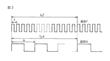
図2は、分周方式の決定を説明する図である。ここでは、波長fを有するマスタークロックに関する波形を波形F、実測画素間隔aに関する波形を波形Aと称する。 FIG. 2 is a diagram for explaining the determination of the frequency division method. Here, a waveform related to the master clock having the wavelength f is referred to as a waveform F, and a waveform related to the measured pixel interval a is referred to as a waveform A.
分周機能は、一般には電子回路として実現されるので、分周方式は電子回路として有限な規模に収める必要がある。ここで、式(7)を満たす任意の正の実数fおよびaに対し、sおよびtを任意の整数とするとき、式(8)を考える。 Since the frequency dividing function is generally realized as an electronic circuit, the frequency dividing method needs to be limited to a finite scale as an electronic circuit. Here, when s and t are arbitrary integers with respect to arbitrary positive real numbers f and a satisfying the expression (7), the expression (8) is considered.
ここで、
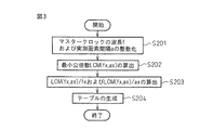
図3は、本発明の実施例における同期信号の生成アルゴリズムを示すフローチャートである。 FIG. 3 is a flowchart showing a synchronization signal generation algorithm in the embodiment of the present invention.
式(8)および(9)において(s0,t0)を求めるということは、マスタークロックの波長fと実測画素間隔aとの最小公倍数を求めることに他ならない。しかしながら、マスタークロックの波長fはレーザ干渉計の出力するパルスの波長であり、実測画素間隔aは光源の実際の間隔Eを上記整数pで除算することで得られる値であるので、マスタークロックの波長fおよび実測画素間隔aはともに実数となる。ともに実数のfおよびaから最小公倍数を算出するの難しいので、本実施例では、まず図3のステップS201において、相互に単位を合わせた上で、マスタークロックの波長fおよび実測画素間隔aの各値を整数化する。より具体的には、fおよびaの単位を例えばnm(ナノメートル)といったように合わせたうえで、有効数字の最小桁が整数となるように、fおよびaに10のべき数を乗算し、これをfxおよびaxとする。例えば、小数点以下3桁まで有効数字があるならば、fおよびaそれぞれに対して10の3乗を乗算してfxおよびaxを得る。 Obtaining (s 0 , t 0 ) in equations (8) and (9) is nothing other than finding the least common multiple of the master clock wavelength f and the measured pixel interval a. However, the wavelength f of the master clock is the wavelength of the pulse output from the laser interferometer, and the measured pixel interval a is a value obtained by dividing the actual interval E of the light source by the integer p. Both the wavelength f and the measured pixel interval a are real numbers. Since it is difficult to calculate the least common multiple from the real numbers f and a, in this embodiment, first, in step S201 in FIG. 3, after the units are matched with each other, each of the master clock wavelength f and the measured pixel interval a Integer value. More specifically, after the units of f and a are adjusted to, for example, nm (nanometer), f and a are multiplied by a power of 10 so that the least significant digit is an integer. Let this be fx and ax. For example, if there are significant figures up to three decimal places, fx and ax are obtained by multiplying f and a by 10 to the third power.
次にステップS202において、fxとaxとの最小公倍数LCM(fx,ax)を算出する。次いでステップS203において、最小公倍数LCM(fx,ax)をfxで除算した値LCM(fx,ax)/fx、および最小公倍数LCM(fx,ax)をaxで除算した値LCM(fx,ax)/axを算出する。図4は、図3の演算処理における数値例を示す図である。この数値例は、マスタークロックの波長fを19.776nm、ならびに、実測画素間隔aを500nm(数値例1)、490nm(数値例2)および510nm(数値例3)と仮定した場合を示している。マスタークロックの波長fは小数点以下の有効数字が3桁であるので、fおよびaに10の3乗を乗算してfxおよびaxを得る。これらfxおよびaxを用いて、図4に示すようなLCM(fx,ax)、LCM(fx,ax)/fxおよびLCM(fx,ax)/axを得る。 Next, in step S202, the least common multiple LCM (fx, ax) of fx and ax is calculated. Next, in step S203, a value LCM (fx, ax) / fx obtained by dividing the least common multiple LCM (fx, ax) by fx, and a value LCM (fx, ax) / fx obtained by dividing the least common multiple LCM (fx, ax) by ax. ax is calculated. FIG. 4 is a diagram illustrating a numerical example in the arithmetic processing of FIG. In this numerical example, the wavelength f of the master clock is assumed to be 19.776 nm, and the measured pixel interval a is assumed to be 500 nm (Numerical Example 1), 490 nm (Numerical Example 2), and 510 nm (Numerical Example 3). . Since the master clock wavelength f has three significant digits after the decimal point, fx and ax are obtained by multiplying f and a by 10 to the third power. Using these fx and ax, LCM (fx, ax), LCM (fx, ax) / fx and LCM (fx, ax) / ax as shown in FIG. 4 are obtained.
そして、ステップS204において、次式(10)を満たす全ての整数tについて、絶対値|s×fx−t×ax|の値が最小となるような整数sを計算し、これを配列要素s〔t〕として配列テーブルを作成し保存する。
図5は、図4の数値例1における配列テーブルを例示する図である。図示された配列テーブルにおいて、例えばs〔1〕=25は、「マスタークロックのパルスの立ち上がりもしくは立ち下がりの数をカウントして、このカウント数が25に達したら、1番目の同期信号を発生させる」と解釈できる。また例えばs〔8〕=202は、「同じくカウント数が202に達したら、8番目の同期信号を発生させる」と解釈できる。 FIG. 5 is a diagram illustrating an array table in Numerical Example 1 of FIG. In the illustrated arrangement table, for example, s [1] = 25 indicates that “the number of rising or falling edges of the master clock pulse is counted, and when this count reaches 25, the first synchronization signal is generated. Can be interpreted. For example, s [8] = 202 can be interpreted as “when the count reaches 202, the eighth synchronization signal is generated”.
したがって、上記配列テーブルを予め作成して露光装置内の所定のメモリに保存しておいて、「マスタークロックのパルスの立ち上がりもしくは立ち下がりの数をカウントし、このカウント数が配列テーブルに保存された値に達した時点で同期信号を発生させる」ようにすれば、「供給手段による補正済み描画データの描画エンジンへの供給のタイミングの基準となる同期信号をマスタークロックに基づいて発生させた」ということになる。 Therefore, the above array table is created in advance and stored in a predetermined memory in the exposure apparatus. “The number of rising or falling edges of the master clock pulse is counted, and this count is stored in the array table. If a synchronization signal is generated when the value is reached ", it is said that" a synchronization signal serving as a reference for the timing of supplying corrected drawing data to the drawing engine by the supply means is generated based on the master clock " It will be.
図6は、図5の配列テーブルを変形して得られるカウントテーブルを例示する図である。 FIG. 6 is a diagram illustrating a count table obtained by modifying the arrangement table of FIG.
図5の配列テーブルは、予め作成して保存しておくs〔t〕値の桁数が非常に大きくなり得ることから大容量のメモリを必要とする。これに対し、図6のカウントテーブルは、このメモリ容量の低減を目的として、図5の配列テーブルに改良を加えたものである。具体的には、図5の配列テーブルにおける配列要素s〔t+1〕とs〔t〕との差分を、図6のカウントテーブルにおける配列要素q〔t〕として保存する。 The arrangement table of FIG. 5 requires a large capacity memory because the number of digits of the s [t] value created and stored in advance can be very large. On the other hand, the count table of FIG. 6 is obtained by improving the arrangement table of FIG. 5 for the purpose of reducing the memory capacity. Specifically, the difference between the array elements s [t + 1] and s [t] in the array table of FIG. 5 is stored as the array element q [t] in the count table of FIG.
図示されたカウントテーブルにおいて、例えばq〔0〕=25は、「マスタークロックのパルスの立ち上がりもしくは立ち下がりの数をカウントして、そのカウント数が25に達したら、1番目の同期信号を発生させる」、また例えばq〔1〕=26は、「2番目の同期信号は、1番目の同期信号を発生させた後、カウント数がさらに26だけ増えたら発生させる」、さらに例えばq〔2〕=25は、「3番目の同期信号は、2番目の同期信号を発生させた後、カウント数がさらに25だけ増えたら発生させる」、といったように解釈できる。そして、618番目の同期信号を発生した後はカウントテーブルの先頭に戻り、カウント数がさらにq〔0〕すなわち25だけ増えたら、619番目の同期信号を発生させる。以後この繰り返しである。 In the illustrated count table, for example, q [0] = 25 indicates that “the number of rising or falling edges of the master clock pulse is counted, and when the count reaches 25, the first synchronization signal is generated. For example, q [1] = 26 means that “the second synchronization signal is generated when the first synchronization signal is generated and then the count number is further increased by 26”, and further, for example, q [2] = 25 can be interpreted as “the third synchronization signal is generated when the second synchronization signal is generated and then the count number is further increased by 25”. Then, after the 618th synchronization signal is generated, the head returns to the head of the count table, and when the count number is further increased by q [0], that is, 25, the 619th synchronization signal is generated. This is repeated thereafter.
このように、図6のカウントテーブルを用いれば、「循環型の分周」が可能となる。また、保存すべきq〔t〕値の桁数は少なくて済むのでメモリ容量の低減を実現できる。 As described above, the “circulation type frequency division” can be performed by using the count table of FIG. 6. In addition, since the number of q [t] values to be stored is small, a reduction in memory capacity can be realized.
図7は、本発明の実施例において、カウントテーブルを用いた同期信号の生成アルゴリズムを示すフローチャートである。 FIG. 7 is a flowchart showing a synchronization signal generation algorithm using a count table in the embodiment of the present invention.
まずはじめにステップS301において、上述のような配列要素q(t)を有するカウントテーブルを作成する。カウントテーブルは図3〜6を参照して説明したように作成し、作成したカウントテーブルは、露光装置を制御するコンピュータ内の記憶装置などに保存しておく。露光処理中は、カウントテーブルは該コンピュータ内の作業メモリにロードされ、以下の各ステップにおける処理に適宜利用されることになる。 First, in step S301, a count table having the array element q (t) as described above is created. The count table is created as described with reference to FIGS. 3 to 6, and the created count table is stored in a storage device in a computer that controls the exposure apparatus. During the exposure process, the count table is loaded into the working memory in the computer and is used as appropriate for the processes in the following steps.
次にステップS302において、同期信号生成のための初期設定として、tを0(ゼロ)にセットする。次にステップS303において、レジスタ(Register)にq(t)をセットする。 In step S302, t is set to 0 (zero) as an initial setting for generating a synchronization signal. In step S303, q (t) is set in the register (Register).
ステップS304では、マスタークロックを受信したか否かが判定される。マスタークロックを受信した場合は、ステップS305へ進み、レジスタ(Register)の値が1つ減る。ステップS306では、レジスタ(Register)が0(ゼロ)になったか否かが判定される。以上のステップS304〜S306を繰り返し実行することで、マスタークロックのパルスの立ち上がりもしくは立ち下がりの数をカウントする処理(単に「カウント処理」と称する。)が実現される。 In step S304, it is determined whether a master clock has been received. When the master clock is received, the process proceeds to step S305, and the value of the register (Register) is decreased by one. In step S306, it is determined whether or not the register (Register) has become 0 (zero). By repeatedly executing the above steps S304 to S306, a process of counting the number of rising or falling edges of the master clock pulse (simply referred to as “counting process”) is realized.
そしてステップS306においてレジスタ(Register)が0(ゼロ)になったと判定されたとき、ステップS307において同期信号を出力する。 When it is determined in step S306 that the register (Register) has become 0 (zero), a synchronization signal is output in step S307.
ステップS308においてtを1つ進める。ステップS309では、ステップS308でセットされたtとLCM(fx,ax)/axとのmodを演算し(すなわち剰余演算)、演算結果をさらにtにセットする。ステップS310では、ステップS309でセットされたtを用いたq(t)が、レジスタ(Register)にセットされる。以上のステップS308〜S310により、カウントテーブルで規定された最終番目の同期信号を発生した後はカウントテーブルの先頭に戻って再び1番目の同期信号発生のためのカウント処理に戻るという、先に説明した「循環型の分周」が実現される。 In step S308, t is incremented by one. In step S309, mod of t and LCM (fx, ax) / ax set in step S308 is calculated (that is, remainder calculation), and the calculation result is further set to t. In step S310, q (t) using t set in step S309 is set in a register (Register). As described above, after generating the last synchronization signal defined in the count table by the above steps S308 to S310, the process returns to the top of the count table and returns to the count process for generating the first synchronization signal. Thus, “circulation-type frequency division” is realized.
図8〜10は、図7のフローチャートに基づいた同期信号の発生アルゴリズムの下で、図4に示した数値例を用いたシミュレーション結果を示す図であり、図8は処理開始直後、図9は最初の同期信号の発生、図10は2番目の同期信号の発生を示す図である。また、図11は、図8〜10におけるシミュレーションを、さらに長時間実行した場合のシミュレーション結果を示す図である。ここでは、該アルゴリズムを図4の3つの数値例についてVerilog言語で記述し、Verilogシミュレータを用いてシミュレーションを行った。図8〜10において、時間軸の目盛りを示す数値(例えば200.00ns)以外の各数値は、カウントテーブルにおけるt(すなわちマスタークロックのパルスの立ち上がりもしくは立ち下がりのカウント数)を示している。図8〜11より、異なる実測画素間隔aごとに、異なる同期信号が作成されていることが分かる。このことは、描画エンジンごとに異なる実測画素間隔aが得られても、各描画エンジンに最適な同期信号を作成できることを意味する。つまり、この同期信号を使えば、補正済み描画データを、各描画エンジンの光源間の実際の間隔に基づいた最適なタイミングで各描画エンジンに供給することができる。 FIGS. 8 to 10 are diagrams showing simulation results using the numerical example shown in FIG. 4 under the synchronization signal generation algorithm based on the flowchart of FIG. Generation of the first synchronization signal, FIG. 10 is a diagram showing generation of the second synchronization signal. Moreover, FIG. 11 is a figure which shows the simulation result at the time of performing the simulation in FIGS. Here, the algorithm is described in the Verilog language for the three numerical examples in FIG. 4, and a simulation is performed using a Verilog simulator. 8 to 10, each numerical value other than the numerical value indicating the scale of the time axis (for example, 200.00 ns) indicates t in the count table (that is, the count number of rising or falling edges of the master clock pulse). 8 to 11, it can be seen that different synchronization signals are created for different measured pixel intervals a. This means that an optimum synchronization signal can be created for each drawing engine even if a different measured pixel interval a is obtained for each drawing engine. In other words, using this synchronization signal, corrected drawing data can be supplied to each drawing engine at an optimal timing based on the actual interval between the light sources of each drawing engine.
図12は、本発明の実施例における露光装置の基本ブロック図である。 FIG. 12 is a basic block diagram of the exposure apparatus in the embodiment of the present invention.
本実施例によれば、露光対象基板(図示せず)を載せたステージ16の相対移動方向に沿って複数の光源(図示せず)が並ぶ設計上の間隔Dが描画データにおける単位画素間隔bの整数p倍となるよう設計された描画エンジン#1〜#N(参照符号30)を用いて露光対象面上に直接露光することで、所望の露光パターンを形成する露光装置1は、補正手段11と、供給手段12と、クロック生成手段13と、同期手段14と、を備える。同期手段14は、第1の演算手段21と、第2の演算手段22と、出力手段23とを備える。
According to this embodiment, the design interval D in which a plurality of light sources (not shown) are arranged along the relative movement direction of the
露光対象基板を載せたステージ16については、ステージコントローラ(図示せず)によって、描画エンジン#1〜#N(参照符号30)に対する相対移動速度Vexが制御される。このステージコントローラは、ステージ16の移動量を検出するための装置として、本実施例ではレーザ干渉計15を有する。レーザ干渉計15は、ステージ16が一定の移動距離fだけ移動するごとに1パルスを出力する。例えばHe−Neガスレーザを用いた場合、その波長は約632.84nmであるので、適切な周波数逓倍器を用いればf=19.776nmを得る。なお、本実施例ではステージの移動量を検出するための装置としてレーザ干渉計15を用いたが、ステージ16のある一定の移動量に対して安定した信号を出力することができる装置であればその他の装置であってもよく、例えばロータリエンコーダを用いた位置検出器などであってもよい。
For the
クロック生成手段13は、レーザ干渉計15の出力結果に基づいて、露光対象基板を載せたステージ16が相対移動速度Vexで相対移動した単位距離fごとに出力されるマスタークロックを生成する。つまり、ステージ16が一定の移動距離fだけ移動するごとにレーザ干渉計15が出力するパルスをマスタークロックとする。
Based on the output result of the
補正手段11は、光源間の設計上の間隔Dと、描画エンジン#1〜#N(参照符号30)ごとに測定された光源間の実際の間隔Eと、の相違(すなわちD≠E)を用いて、描画エンジン#1〜#N(参照符号30)ごとに描画データを補正し、描画エンジン#1〜#N(参照符号30)ごとの補正済み描画データを生成する。
The
同期手段14は、供給手段12による補正済み描画データの描画エンジン#1〜#N(参照符号30)への供給のタイミングの基準となる同期信号を、描画エンジン#1〜#N(参照符号30)ごとに、マスタークロックに基づいて生成する。より具体的には次のとおりである。
The
同期手段14内の第1の演算手段21は、相互に単位を合わせた、実測画素間隔aと、周期的に出力されるマスタークロックの波長fと、の最小公倍数LCM(f,a)を算出する。この最小公倍数LCM(f,a)は、描画エンジン#1〜#N(参照符号30)ごとの実測画素間隔aを用いて、描画エンジン#1〜#N(参照符号30)ごとに算出される。
The first calculating means 21 in the synchronizing means 14 calculates the least common multiple LCM (f, a) of the measured pixel interval a and the wavelength f of the master clock that is periodically output, with the units mutually matched. To do. This least common multiple LCM (f, a) is calculated for each
同期手段14内の第2の演算手段22は、ゼロから最小公倍数LCM(f,a)を実測画素間隔aで除算した値LCM(f,a)/aまでの範囲に属する各整数をtとしたとき、絶対値|s〔t〕×f−t×a|の値が最小となる配列要素s〔t〕を、各整数tについて算出し、上記配列テーブルもしくは上記カウントテーブルを作成する。この上記配列テーブルもしくは上記カウントテーブルは、描画エンジン#1〜#N(参照符号30)ごとの最小公倍数LCM(f,a)を用いて、描画エンジン#1〜#N(参照符号30)ごとに作成される。作成された上記配列テーブルもしくは上記カウントテーブルは、同期手段14内の記録媒体(ROM)に保存される。
The second calculating means 22 in the synchronizing means 14 calculates each integer belonging to a range from zero to a value LCM (f, a) / a obtained by dividing the least common multiple LCM (f, a) by the measured pixel interval a and t. Then, the array element s [t] having the minimum absolute value | s [t] × f−t × a | is calculated for each integer t, and the array table or the count table is created. The array table or the count table is used for each
出力手段23は、作成された上記配列テーブルもしくは上記カウントテーブルを参照して、マスタークロックのパルスの立ち上がりもしくは立ち下がりの数を所定の値までカウントしたときに、同期信号を供給手段12へ出力する。この同期信号は、描画エンジン#1〜#N(参照符号30)ごとの上記配列テーブルもしくは上記カウントテーブルを用いて、描画エンジン#1〜#N(参照符号30)ごとの同期信号として供給手段12へ出力される。
The
供給手段12は、同期手段14内の出力手段23から受信した描画エンジン#1〜#N(参照符号30)ごとの同期信号に基づいて、描画エンジン#1〜#N(参照符号30)のそれぞれが一度に露光可能な露光対象面上の露光ブロックへの直接露光に必要な分だけの、描画エンジン#1〜#N(参照符号30)ごとの補正済み描画データを、対応する描画エンジン#1〜#N(参照符号30)へ供給する。同期手段14内の出力手段23から受信した同期信号に従えば、光源間の実際の間隔Eを上記整数pで除算することで得られる実測画素間隔aに相当する距離だけ露光対象基板を載せたステージ16が相対移動するごとの、補正済み描画データの供給が可能となる。
Based on the synchronization signal for each
各描画エンジン#1〜#N(参照符号30)には、補正手段11によって生成された描画エンジン#1〜#N(参照符号30)ごとの補正済み描画データが、光源間の実際の間隔Eで規定される描画エンジン#1〜#N(参照符号30)ごとのタイミングで、供給手段12から供給される。各描画エンジン#1〜#N(参照符号30)は、供給された補正済み描画データ補正済み描画データに基づいて直接露光処理を実行する。
In each of the
上述の実施例では、同期信号を、配列テーブルもしくはカウントテーブルを用いて生成した。この場合、実測画素間隔aとマスタークロックの波長fとの最小公倍数LCM(f,a)を算出する際は、相互に単位を合わせ、有効数字の最小桁が整数となるようにしていた。つまり、fおよびaの単位を例えばnm(ナノメートル)といったように合わせたうえで、有効数字の最小桁が整数となるようにマスタークロックの波長fおよび実測画素間隔aに10のべき数を乗算し、整数化されたfxおよびaxについて最小公倍数を求めていた。しかし、高精度の配線パターンの生成が要求される場合などでは、マスタークロックの波長fおよび/または実測画素間隔aの小数点以下の有効数字の桁数も大きくなり、上述のような整数化を行うとfxおよびaxは非常に大きな値となる。このため、同期信号の生成に配列テーブルではなくカウントテーブルを用いたとしても、大容量のメモリが必要となる。ここで、高精度の配線パターンの生成であっても大容量のメモリを必要としない同期信号の生成アルゴリズムの変形例を説明する。 In the above-described embodiment, the synchronization signal is generated using the arrangement table or the count table. In this case, when calculating the least common multiple LCM (f, a) of the measured pixel interval a and the master clock wavelength f, the units are mutually matched so that the least significant digit is an integer. That is, after the unit of f and a is adjusted to, for example, nm (nanometer), the master clock wavelength f and the measured pixel interval a are multiplied by a power of 10 so that the least significant digit is an integer. Then, the least common multiple was obtained for integerized fx and ax. However, when generation of a highly accurate wiring pattern is required, the number of significant digits after the decimal point of the master clock wavelength f and / or the measured pixel interval a is increased, and the above-described integerization is performed. And fx and ax are very large values. For this reason, even if a count table is used instead of an array table for generating a synchronization signal, a large-capacity memory is required. Here, a modified example of a synchronization signal generation algorithm that does not require a large-capacity memory even when generating a highly accurate wiring pattern will be described.
本変形例による同期手段は、
マスタークロックの波長の積算値を格納するための第1の積算手段と、
マスタークロックを受信したとき、第1の積算手段に格納されているマスタークロックの波長の積算値に、マスタークロックの波長をさらに加算する第1の加算手段と、
実測画素間隔の積算値を格納するための第2の積算手段と、
第1の積算手段に格納されているマスタークロックの波長の積算値と、第2の積算手段に格納されている実測画素間隔の積算値と、の減算値の絶対値を算出する減算手段と、
上記減算値の絶対値とマスタークロックの波長との大小関係を判定する判定手段と、
判定手段が、上記減算値の絶対値の方がマスタークロックの波長よりも小さいと判定したとき、同期信号を出力する出力手段と、
判定手段が、上記減算値の絶対値の方がマスタークロックの波長よりも小さいと判定したときに、第2の積算手段に格納されている実測画素間隔の積算値に、実測画素間隔をさらに加算する第2の加算手段と、
を有する。
The synchronization means according to this modification is
First integrating means for storing the integrated value of the wavelength of the master clock;
First addition means for further adding the wavelength of the master clock to the integrated value of the wavelength of the master clock stored in the first integration means when the master clock is received;
A second integration means for storing an integrated value of the measured pixel intervals;
A subtracting means for calculating an absolute value of a subtraction value between the integrated value of the wavelength of the master clock stored in the first integrating means and the integrated value of the measured pixel interval stored in the second integrating means;
A determination means for determining a magnitude relationship between the absolute value of the subtraction value and the wavelength of the master clock;
When the determination unit determines that the absolute value of the subtraction value is smaller than the wavelength of the master clock, an output unit that outputs a synchronization signal;
When the determination unit determines that the absolute value of the subtraction value is smaller than the wavelength of the master clock, the actual pixel interval is further added to the integrated value of the actual pixel interval stored in the second integration unit. Second adding means for
Have
図13は、本発明の実施例における同期信号の生成アルゴリズムの変形例を示すフローチャートである。また、図14は、図13のフローチャートに基づいた同期信号を出力する同期手段を示す機能ブロック図である。 FIG. 13 is a flowchart showing a modification of the synchronization signal generation algorithm in the embodiment of the present invention. FIG. 14 is a functional block diagram showing synchronization means for outputting a synchronization signal based on the flowchart of FIG.
図14に示すように、本変形例による同期手段14は、上記の第1の加算手段である加算器42と、上記の第2の加算手段である加算器43と、上記の第1の積算手段(アキュムレータ)44と、上記の第2の積算手段(アキュムレータ)45と、上記の減算手段である減算器46と、上記の判定手段であるコンパレータ47と、を備える。また、同期手段14は、マスタークロックの波長fに相当する数値を記憶する第1のレジスタ40と、実測画素間隔aに相当する数値を記憶する第2のレジスタ41とを備える。
As shown in FIG. 14, the synchronization means 14 according to this modification includes an
本変形例では、まず、図13のステップS401において、初期化処理として、図14の第1の積算手段44に格納されるマスタークロックの波長fの積算値Afを0(ゼロ)にセットし、第2の積算手段45に格納される実測画素間隔aの積算値Aaをaにセットする。すなわち、初期状態では、Af<<Aaである。
In this modification, first, in step S401 of FIG. 13, as an initialization process, the integrated value Af of the wavelength f of the master clock stored in the first integrating
ステージ16が移動を開始するとマスタークロックが供給され始める。ステップS402においてマスタークロックを受信すると、ステップS403において、第1の積算手段44に格納されているマスタークロックの波長の積算値Afに、第1のレジスタ40に記憶されているマスタークロックの波長fが加算器42によって加算され、新たなる積算値Afが第1の積算手段44に格納される。
When the
次いで、ステップS404において、減算器46は、第1の積算手段44に格納されているマスタークロックの波長の積算値Afと、第2の積算手段45に格納されている実測画素間隔の積算値Aaと、の減算値の絶対値|Af−Aa|を算出する。
Next, in step S <b> 404, the
次いで、ステップS405において、判定手段47は、減算器46によって算出された上記減算値の絶対値|Af−Aa|と、第1のレジスタ40に記憶されているマスタークロックの波長fと、の大小関係を判定する。判定手段47が、上記減算値の絶対値|Af−Aa|の方がマスタークロックの波長fよりも大きいと判定した場合はステップS402へ戻る。
Next, in step S405, the
判定手段47が、上記減算値の絶対値|Af−Aa|の方がマスタークロックの波長fよりも小さいと判定したときは、ステップS406へ進み、同期信号を出力する。ステップS407では、第2の積算手段45に格納されている実測画素間隔の積算値Aaに、第2のレジスタ41に記憶されている実測画素間隔aが加算器43によって加算され、新たなる積算値Aaが第2の積算手段45に格納される。なお、ステップS406とステップS407とを入れ替えて実行するようにしてもよく、あるいは同時に実行してもよい。
When the
以上の処理をまとめると、本変形例による同期手段14では、受信したマスタークロックをトリガーにして、マスタークロックの波長fを積算していき、マスタークロックの波長の積算値Afが、実測画素間隔の積算値Aaに最も近くなったときにだけ、同期信号を出力する。そして、同期信号の出力と同時に、実測画素間隔の積算値Aaに、実測画素間隔aがさらに加算され、これが新たなる実測画素間隔の積算値Aaとなる。以後、同様の処理が繰り返される。すなわち、マスタークロックの受信ごとに積算されるマスタークロックの波長の積算値Afが上記新たなる実測画素間隔の積算値Aaに最も近くなったときに、同期信号が出力されるとともに実測画素間隔aが実測画素間隔の積算値Aaに加算される。つまり、上記各加算処理のタイミングは異なり、マスタークロックの波長fの積算値Afへの加算は、マスタークロックの受信ごとに行われ、実測画素間隔aの積算値Aaへの加算は、マスタークロックの波長の積算値Afが実測画素間隔の積算値Aaに最も近くなったときに行われる。図15は、図13のフローチャートに基づいた同期信号の生成のタイミングチャートの一例を示す図である。この図では、波長fを有するマスタークロックに関する波形を波形Fとしたときの同期信号の発生を例示する。なお、ステージ16が移動して露光処理が露光対象基板の端に到達すると、マスタークロックの供給は停止され、第1の積算手段44に格納されているマスタークロックの波長の積算値Afおよび第2の積算手段45に格納されている実測画素間隔の積算値Aaはリセットされる。
To summarize the above processing, the synchronization means 14 according to the present modification integrates the master clock wavelength f using the received master clock as a trigger, and the master clock wavelength integrated value Af is the measured pixel interval. A synchronization signal is output only when the value is closest to the integrated value Aa. Simultaneously with the output of the synchronization signal, the actual pixel interval a is further added to the integrated value Aa of the actual pixel interval, and this becomes the new integrated value Aa of the actual pixel interval. Thereafter, the same processing is repeated. That is, when the integrated value Af of the wavelength of the master clock integrated every time the master clock is received becomes closest to the integrated value Aa of the new measured pixel interval, the synchronization signal is output and the measured pixel interval a is It is added to the integrated value Aa of the measured pixel interval. That is, the timing of each addition process is different, and the addition of the master clock wavelength f to the integrated value Af is performed every time the master clock is received, and the addition of the measured pixel interval a to the integrated value Aa is This is performed when the integrated value Af of the wavelength is closest to the integrated value Aa of the measured pixel interval. FIG. 15 is a diagram illustrating an example of a timing chart for generating a synchronization signal based on the flowchart of FIG. This figure illustrates the generation of a synchronization signal when the waveform relating to the master clock having the wavelength f is the waveform F. When the
このように、本変形例は、同期信号の発生要件を数式化してそれを一般的なディジタル回路(レジスタ、加算器、アキュムレータ、減算器およびコンパレータ)で実現したものであり、先に説明した実施例における配列テーブルもしくはカウントテーブルの生成や最小公倍数の計算は不要である。なお、レジスタ、加算器、アキュムレータ、減算器およびコンパレータが扱う値は、実数(固定小数点数)に限らず、浮動小数点数であってもよい。 As described above, this modification example formulates the generation requirement of the synchronization signal and realizes it with a general digital circuit (register, adder, accumulator, subtractor, and comparator). There is no need to generate an array table or count table or calculate the least common multiple in the example. Note that the values handled by the register, adder, accumulator, subtractor, and comparator are not limited to real numbers (fixed-point numbers) but may be floating-point numbers.
本変形例の具体的な一数値例を挙げると次の通りである。すなわち、レジスタ、加算器、アキュムレータ、減算器およびコンパレータを整数のみを扱うとした例では、マスタークロックの波長fおよび実測画素間隔aの値の小数点以下を必要な精度だけ桁上げして整数化し、これを第1のレジスタ40および第2のレジスタ41にそれぞれ記憶する。例えば、f=19.776252201nm、a=490.000000000nmとする場合、それぞれ、fx=19776252201、ax=490000000000といった非常に桁数の大きい整数に置換する。ここで露光対象基板が乗るステージがL=1mの距離を移動すると仮定すると、L/a(≒204万)個の同期信号が発生するから、第2の積算値45に格納される実測画素間隔の積算値Aaは、約1×1018の大きさに達する。このため、レジスタ、加算器、アキュムレータ、減算器およびコンパレータは、約64ビットのデータ処理能力が必要となるが、このような規模のディジタル回路であっても、FPGAデバイスなどを使用すれば、必要な機能は十分かつ容易に実現可能である。
A specific numerical example of this modification is as follows. That is, in the example in which the register, adder, accumulator, subtractor, and comparator handle only integers, the decimal point of the value of the master clock wavelength f and the measured pixel interval a is raised to the required precision to be converted into an integer, This is stored in the
なお、図14の第1のレジスタ40に記憶されるマスタークロックの波長fについては外部から書き換えることも容易であり、例えばレーザ干渉計以外の基準信号源をマスタークロックにすることも可能である。
The wavelength f of the master clock stored in the
同様に、第2のレジスタ41に記憶される実測画素間隔aの値についても外部から書き換えることも容易であり、回路構成を変更することなく実測画素間隔aを任意に変更することも可能である。さらにまた、複数の異なる実測画素間隔aの値が必要となる場合は、第1のレジスタ40および第1の積算手段44については共通にしておいて、第2のレジスタ41および第2の積算手段45については実測画素間隔aごとに設ければよい。
Similarly, the value of the measured pixel interval a stored in the second register 41 can be easily rewritten from the outside, and the measured pixel interval a can be arbitrarily changed without changing the circuit configuration. . Furthermore, when a plurality of different measured pixel intervals a are required, the
上述の露光装置1における補正手段11、供給手段12、クロック生成手段13、および同期手段14は、コンピュータ等の演算処理装置が実行することができるソフトウェアプログラムおよびハードウェアの組合せで実現できる。また、各処理をコンピュータにより実行させるプログラムを記録媒体に格納し、必要に応じて該コンピュータ内の作業メモリにロードされ、実行される。
The
以上、実施例として露光装置について説明したが、その他の描画ヘッドが所定の間隔で複数配列され、描画対象物が描画ヘッドに対して相対移動していくことで描画処理する描画装置についてもまったく同じ原理を適用することができる。このような描画装置の例としてインクジェット描画装置あるいはレーザプリンタのような印刷装置などがある。 As described above, the exposure apparatus has been described as an example. However, the same applies to a drawing apparatus in which a plurality of other drawing heads are arranged at predetermined intervals and a drawing target moves relative to the drawing head. The principle can be applied. Examples of such a drawing device include an ink jet drawing device or a printing device such as a laser printer.
このうち、インクジェット技術を用いたインクジェット描画装置は、インクジェットノズルが所定の設計間隔でインクジェットヘッド内に複数配列され、描画対象物がインクジェットヘッドに対して相対移動していくことで描画処理する装置であり、近年、基板に描画パターンを直接描画(パターニング)する手段として有望視されている。 Among them, an ink jet drawing apparatus using ink jet technology is an apparatus that performs drawing processing by arranging a plurality of ink jet nozzles in an ink jet head at a predetermined design interval and moving a drawing object relative to the ink jet head. In recent years, it is considered promising as a means for directly drawing (patterning) a drawing pattern on a substrate.
インクジェット技術は、液滴を小さい穴の開いたノズルから吐出する技術である。このインクジェット技術は、一般にプリンタに用いられることが多いが、インクジェットパターニングに適用する場合は、ノズルから吐出する液滴を金属微粒子を含む液体や金属酸化物材料とすればよい。なお、インクジェット技術は、電圧を加えると変形する圧電素子を使い、瞬間的にインク室の液圧を高めることでノズルから液滴を押し出すピエゾ式と、ヘッドに取り付けたヒータによって、液体内に気泡を発生させ、液体を押し出すサーマル式とに大別されるが、どちらの場合も本発明に適用可能である。インクジェット描画装置に本発明を適用する場合は、上述の本発明の実施例における露光ヘッドすなわち光源を、インクジェットヘッドに置き換えればよい。 The ink jet technique is a technique for ejecting droplets from a nozzle having a small hole. In general, this ink-jet technique is often used in a printer. However, when applied to ink-jet patterning, a liquid droplet containing metal fine particles or a metal oxide material may be used as a droplet discharged from a nozzle. Inkjet technology uses a piezoelectric element that deforms when a voltage is applied, and instantaneously increases the fluid pressure in the ink chamber to push droplets out of the nozzle, and a heater attached to the head creates bubbles in the liquid. And is divided roughly into a thermal type that extrudes a liquid, and both cases are applicable to the present invention. When the present invention is applied to an ink jet drawing apparatus, the exposure head, that is, the light source in the above-described embodiment of the present invention may be replaced with an ink jet head.
描画対象面上を相対移動する描画ヘッドが一度に描画可能な描画対象面上の描画ブロックへの直接描画処理に必要な描画データが、設計データに基づいて順次生成され、描画エンジンに順次供給される描画装置に適用することができる。本発明は、描画装置がマスクレス露光装置であってもインクジェット描画装置であってもどちらでも適用可能である。 The drawing data required for direct drawing processing to the drawing block on the drawing target surface that can be drawn at once by the drawing head that moves relative to the drawing target surface is sequentially generated based on the design data and is supplied to the drawing engine sequentially. It can be applied to a drawing apparatus. The present invention can be applied regardless of whether the drawing apparatus is a maskless exposure apparatus or an inkjet drawing apparatus.
直接描画によるパターニング方法によれば、高精度な配線の設計、検査および形成を容易かつ高速に行うことができ、また、位置合わせのためのマージンが少なく済むので配線の実装密度が上がる。したがって、将来の超微細配線にも十分に対応可能である。また、設計データを適宜加工して補正情報を蓄積していき、動的(ダイナミック)に補正およびルーティングを実行でき、設計変更にも柔軟に対応できるという利点がある。 According to the patterning method by direct drawing, high-accuracy wiring can be designed, inspected, and formed easily and at a high speed, and a margin for alignment is reduced, so that the wiring mounting density is increased. Therefore, it can sufficiently cope with future ultra-fine wiring. In addition, there is an advantage that design data is appropriately processed and correction information is accumulated, correction and routing can be executed dynamically, and design changes can be flexibly handled.
本発明による描画システムによれば、描画装置内の他の諸機能への新たな負担を強いることなく、かつ、演算処理量の大幅な増加を伴うことなく、描画装置内の描画エンジンの製造ばらつきに起因する解像能力の格差を解消し、高解像能力を実現することができるので、特に高精度が要求される複雑な配線パターンを形成する際に最適である。 According to the drawing system according to the present invention, the manufacturing variation of the drawing engine in the drawing apparatus without imposing a new burden on other functions in the drawing apparatus and without significantly increasing the calculation processing amount. It is possible to eliminate the disparity in resolution ability caused by the above and realize a high resolution ability, which is particularly suitable when forming a complicated wiring pattern requiring high accuracy.
1 描画装置
11 補正手段
12 供給手段
13 クロック生成手段
14 同期手段
15 レーザ干渉計
16 ステージ
21 第1の演算手段
22 第2の演算手段
23 出力手段
30 描画エンジン
DESCRIPTION OF
Claims (9)
前記設計上の間隔と、前記複数の描画素子が並ぶ実際の間隔と、の相違を用いて前記描画データを補正して補正済み描画データを生成する補正手段と、
前記実際の間隔を前記整数で除算することで得られる実測画素間隔に相当する距離だけ前記描画対象面が相対移動するごとに、前記描画エンジンが一度に描画可能な前記描画対象面上の描画ブロックへの直接描画に必要な分だけの前記補正済み描画データを、前記描画エンジンへ供給する供給手段と、
を備え、
前記補正済み描画データに基づいた描画パターンを形成することを特徴とする描画装置。 Drawing directly on the drawing target surface using a drawing engine designed such that the design interval in which a plurality of drawing elements are arranged along the relative movement direction of the drawing target surface is an integral multiple of the unit pixel interval in the drawing data. Thus, a drawing apparatus for forming a desired drawing pattern,
Correction means for correcting the drawing data using a difference between the design interval and an actual interval in which the plurality of drawing elements are arranged to generate corrected drawing data;
A drawing block on the drawing target surface on which the drawing engine can draw at a time each time the drawing target surface relatively moves by a distance corresponding to an actually measured pixel interval obtained by dividing the actual interval by the integer. Supply means for supplying the corrected drawing data as much as necessary for direct drawing to the drawing engine;
With
A drawing apparatus that forms a drawing pattern based on the corrected drawing data.
前記供給手段による前記補正済み描画データの前記描画エンジンへの供給のタイミングの基準となる同期信号を、前記マスタークロックに基づいて生成する同期手段と、
をさらに備える請求項1に記載の描画装置。 A clock generating means for generating a master clock that is output for each unit distance in which the drawing target surface is relatively moved;
Synchronization means for generating a synchronization signal as a reference of the timing of supply of the corrected drawing data to the drawing engine by the supply means based on the master clock;
The drawing apparatus according to claim 1, further comprising:
相互に単位を合わせた、前記実測画素間隔と、周期的に出力される前記マスタークロックの波長と、の最小公倍数を算出する第1の演算手段と、
ゼロから前記最小公倍数を前記実測画素間隔で除算した値までの範囲に属する各整数をt、前記実測画素間隔をa、前記マスタークロックの波長をfとしたとき、
絶対値|s〔t〕×f−t×a|の値が最小となる配列要素s〔t〕を、各前記整数tについて算出する第2の演算手段と、
前記マスタークロックを前記第2の演算手段で算出された前記配列要素s〔t〕の値までカウントしたときに、前記同期信号を出力する出力手段と、を有する請求項3に記載の描画装置。 The synchronization means includes
First arithmetic means for calculating a least common multiple of the measured pixel interval and the wavelength of the master clock periodically output, the units of which are mutually matched;
When each integer belonging to a range from zero to a value obtained by dividing the least common multiple by the measured pixel interval is t, the measured pixel interval is a, and the wavelength of the master clock is f,
A second computing means for calculating an array element s [t] for which the absolute value | s [t] × f−t × a |
The drawing apparatus according to claim 3, further comprising: an output unit that outputs the synchronization signal when the master clock is counted up to the value of the array element s [t] calculated by the second calculation unit.
前記マスタークロックの波長の積算値を格納するための第1の積算手段と、
前記マスタークロックを受信したとき、前記第1の積算手段に格納されている前記マスタークロックの波長の積算値に、前記マスタークロックの波長をさらに加算する第1の加算手段と、
前記実測画素間隔の積算値を格納するための第2の積算手段と、
前記第1の積算手段に格納されている前記マスタークロックの波長の積算値と、前記第2の積算手段に格納されている前記実測画素間隔の積算値と、の減算値の絶対値を算出する減算手段と、
前記減算値の絶対値と前記マスタークロックの波長との大小関係を判定する判定手段と、
該判定手段が、前記減算値の絶対値の方が前記マスタークロックの波長よりも小さいと判定したとき、前記同期信号を出力する出力手段と、
前記判定手段が、前記減算値の絶対値の方が前記マスタークロックの波長よりも小さいと判定したときに、前記第2の積算手段に格納されている前記実測画素間隔の積算値に、前記実測画素間隔をさらに加算する第2の加算手段と、
を有する請求項3に記載の描画装置。 The synchronization means includes
First integrating means for storing an integrated value of the wavelength of the master clock;
First addition means for further adding the wavelength of the master clock to the integrated value of the wavelength of the master clock stored in the first integration means when the master clock is received;
A second integrating means for storing an integrated value of the measured pixel interval;
An absolute value of a subtraction value between the integrated value of the wavelength of the master clock stored in the first integrating means and the integrated value of the measured pixel interval stored in the second integrating means is calculated. Subtracting means;
Determination means for determining a magnitude relationship between the absolute value of the subtraction value and the wavelength of the master clock;
When the determination means determines that the absolute value of the subtraction value is smaller than the wavelength of the master clock, output means for outputting the synchronization signal;
When the determination unit determines that the absolute value of the subtraction value is smaller than the wavelength of the master clock, the measured value is added to the integrated value of the measured pixel interval stored in the second integrating unit. Second addition means for further adding pixel intervals;
The drawing apparatus according to claim 3.
前記補正手段は、前記描画エンジンごとに測定された前記実際の間隔を用いて、前記描画エンジンごとに前記補正済み描画データを生成し、
前記供給手段は、前記補正手段によって生成された前記描画エンジンごとの前記補正済み描画データを、対応する前記描画エンジンに供給する請求項1に記載の描画装置。 The drawing apparatus includes a plurality of the drawing engines,
The correction means generates the corrected drawing data for each drawing engine using the actual interval measured for each drawing engine,
The drawing apparatus according to claim 1, wherein the supply unit supplies the corrected drawing data for each drawing engine generated by the correction unit to the corresponding drawing engine.
前記同期手段は、前記描画エンジンごとに前記同期信号を生成する請求項3〜5のいずれか一項に記載の描画装置。 The drawing apparatus includes a plurality of the drawing engines,
The drawing apparatus according to claim 3, wherein the synchronization unit generates the synchronization signal for each drawing engine.
前記設計上の間隔と、前記複数の描画素子が並ぶ実際の間隔と、の相違を用いて前記描画データを補正して補正済み描画データを生成する補正ステップと、
前記実際の間隔を前記整数で除算することで得られる実測画素間隔に相当する距離だけ前記描画対象面が相対移動するごとに、前記描画エンジンが一度に描画可能な前記描画対象面上の描画ブロックへの直接描画に必要な分だけの前記補正済み描画データを、前記描画エンジンへ供給する供給ステップと、
を備え、
前記補正済み描画データに基づいた描画パターンを形成することを特徴とする描画方法。 Drawing directly on the drawing target surface using a drawing engine designed such that the design interval in which a plurality of drawing elements are arranged along the relative movement direction of the drawing target surface is an integral multiple of the unit pixel interval in the drawing data. A drawing method for forming a desired drawing pattern,
A correction step of correcting the drawing data using a difference between the design interval and an actual interval in which the plurality of drawing elements are arranged to generate corrected drawing data;
A drawing block on the drawing target surface on which the drawing engine can draw at a time each time the drawing target surface relatively moves by a distance corresponding to an actually measured pixel interval obtained by dividing the actual interval by the integer. Supplying the corrected drawing data as much as necessary for direct drawing to the drawing engine;
With
A drawing method comprising forming a drawing pattern based on the corrected drawing data.
Priority Applications (4)
| Application Number | Priority Date | Filing Date | Title |
|---|---|---|---|
| JP2005126614A JP4601482B2 (en) | 2004-07-29 | 2005-04-25 | Drawing apparatus and drawing method |
| TW094125234A TWI368184B (en) | 2004-07-29 | 2005-07-26 | Drawing apparatus and drawing method |
| US11/191,021 US7266802B2 (en) | 2004-07-29 | 2005-07-28 | Drawing apparatus and drawing method |
| KR1020050068956A KR101135601B1 (en) | 2004-07-29 | 2005-07-28 | Drawing apparatus and drawing method |
Applications Claiming Priority (2)
| Application Number | Priority Date | Filing Date | Title |
|---|---|---|---|
| JP2004221778 | 2004-07-29 | ||
| JP2005126614A JP4601482B2 (en) | 2004-07-29 | 2005-04-25 | Drawing apparatus and drawing method |
Publications (3)
| Publication Number | Publication Date |
|---|---|
| JP2006066877A JP2006066877A (en) | 2006-03-09 |
| JP2006066877A5 JP2006066877A5 (en) | 2008-04-03 |
| JP4601482B2 true JP4601482B2 (en) | 2010-12-22 |
Family
ID=35731611
Family Applications (1)
| Application Number | Title | Priority Date | Filing Date |
|---|---|---|---|
| JP2005126614A Expired - Lifetime JP4601482B2 (en) | 2004-07-29 | 2005-04-25 | Drawing apparatus and drawing method |
Country Status (4)
| Country | Link |
|---|---|
| US (1) | US7266802B2 (en) |
| JP (1) | JP4601482B2 (en) |
| KR (1) | KR101135601B1 (en) |
| TW (1) | TWI368184B (en) |
Families Citing this family (10)
| Publication number | Priority date | Publication date | Assignee | Title |
|---|---|---|---|---|
| JP5001638B2 (en) * | 2006-12-22 | 2012-08-15 | 株式会社オーク製作所 | Exposure data creation device |
| JP5020745B2 (en) * | 2007-08-29 | 2012-09-05 | 株式会社ニューフレアテクノロジー | Drawing data creation method and charged particle beam drawing apparatus |
| JP5215018B2 (en) * | 2008-03-28 | 2013-06-19 | 大日本スクリーン製造株式会社 | Image recording device |
| KR101095549B1 (en) | 2010-04-29 | 2011-12-19 | 삼성전자주식회사 | Maskless exposure apparatus and stitching exposure method using the same |
| CN103699708A (en) * | 2013-05-14 | 2014-04-02 | 上海大众汽车有限公司 | Fully parametric drawing mould design method |
| GB2517702A (en) * | 2013-08-28 | 2015-03-04 | Ibm | Collaborative electronic nose management in personal devices |
| CN109803096B (en) * | 2019-01-11 | 2020-08-25 | 北京大学 | Display method and system based on pulse signals |
| US11228758B2 (en) * | 2016-01-22 | 2022-01-18 | Peking University | Imaging method and device |
| US12452416B2 (en) | 2016-01-22 | 2025-10-21 | Spike Vision (Beijing) Technology Co., Ltd. | Generating image based on pulse sequences obtained from encoded information |
| JP2024119436A (en) * | 2023-02-22 | 2024-09-03 | 株式会社Screenホールディングス | Drawing device |
Family Cites Families (15)
| Publication number | Priority date | Publication date | Assignee | Title |
|---|---|---|---|---|
| CA2075026A1 (en) * | 1991-08-08 | 1993-02-09 | William E. Nelson | Method and apparatus for patterning an imaging member |
| US6074790A (en) * | 1994-11-17 | 2000-06-13 | Texas Instruments Incorporated | Black and white defect correction for a digital micromirror printer |
| JPH10112579A (en) | 1996-10-07 | 1998-04-28 | M S Tec:Kk | Resist exposing method and exposing apparatus |
| SE516914C2 (en) * | 1999-09-09 | 2002-03-19 | Micronic Laser Systems Ab | Methods and grid for high performance pattern generation |
| JP2001255664A (en) * | 2000-03-14 | 2001-09-21 | Fuji Photo Film Co Ltd | Image exposing method |
| DE10031915A1 (en) * | 2000-06-30 | 2002-01-10 | Heidelberger Druckmasch Ag | Compact multi-beam laser light source and interleaved scanning line method for exposure of printing plates |
| US6998219B2 (en) * | 2001-06-27 | 2006-02-14 | University Of South Florida | Maskless photolithography for etching and deposition |
| JP4320694B2 (en) * | 2001-08-08 | 2009-08-26 | 株式会社オーク製作所 | Multiple exposure drawing apparatus and multiple exposure drawing method |
| JP4273291B2 (en) * | 2001-08-17 | 2009-06-03 | 株式会社オーク製作所 | Multiple exposure drawing apparatus and multiple exposure drawing method |
| US20030186164A1 (en) * | 2002-03-27 | 2003-10-02 | Hitachi, Ltd. | Information recording medium, a method for recording information and a method for manufacturing a medium |
| JP4274784B2 (en) * | 2002-05-28 | 2009-06-10 | 新光電気工業株式会社 | Wiring forming system and method thereof |
| JP2004012899A (en) * | 2002-06-07 | 2004-01-15 | Fuji Photo Film Co Ltd | Aligner |
| CN101487982A (en) * | 2002-08-24 | 2009-07-22 | 无掩模平版印刷公司 | Continuous direct-write optical lithography |
| JP4150250B2 (en) * | 2002-12-02 | 2008-09-17 | 富士フイルム株式会社 | Drawing head, drawing apparatus and drawing method |
| US7061591B2 (en) * | 2003-05-30 | 2006-06-13 | Asml Holding N.V. | Maskless lithography systems and methods utilizing spatial light modulator arrays |
-
2005
- 2005-04-25 JP JP2005126614A patent/JP4601482B2/en not_active Expired - Lifetime
- 2005-07-26 TW TW094125234A patent/TWI368184B/en not_active IP Right Cessation
- 2005-07-28 US US11/191,021 patent/US7266802B2/en active Active
- 2005-07-28 KR KR1020050068956A patent/KR101135601B1/en not_active Expired - Lifetime
Also Published As
| Publication number | Publication date |
|---|---|
| TW200622935A (en) | 2006-07-01 |
| KR101135601B1 (en) | 2012-04-17 |
| US7266802B2 (en) | 2007-09-04 |
| US20060022982A1 (en) | 2006-02-02 |
| TWI368184B (en) | 2012-07-11 |
| JP2006066877A (en) | 2006-03-09 |
| KR20060048868A (en) | 2006-05-18 |
Similar Documents
| Publication | Publication Date | Title |
|---|---|---|
| JP4601482B2 (en) | Drawing apparatus and drawing method | |
| CN102483577B (en) | Rotor Imaging System and Method Using Variable Rate Pixel Clock | |
| US20030160980A1 (en) | Graphics engine for high precision lithography | |
| CN101135862A (en) | Drawings device and drawing method | |
| TWI853927B (en) | Drift correction method and system | |
| US8137875B2 (en) | Method and apparatus for overlay compensation between subsequently patterned layers on workpiece | |
| CN104199257A (en) | Method for measuring and compensating absolute positioning accuracy of precise positioning platform | |
| CN107945130A (en) | A kind of projection malformation correction method of photocuring 3D printer | |
| CN101194209A (en) | Exposure device | |
| JP2005521253A (en) | Method and apparatus for printing large data flows | |
| US20120198395A1 (en) | Flare value calculation method, flare correction method, and computer program product | |
| JP2014056167A (en) | Patterning apparatus, patterning method, and production method of display panel substrate | |
| KR101182698B1 (en) | Image recording processing circuit, image recording apparatus and image recording method using image recording processing circuit | |
| KR101261353B1 (en) | Plotting point data acquisition method and device, plotting method and device | |
| CN114253490B (en) | Inkjet printing method, inkjet printing apparatus, electronic device, and computer-readable storage medium | |
| JPS5840826A (en) | Charged beam exposure | |
| WO2006112484A1 (en) | Convey error measuring method, calibration method, plotting method, exposure plotting method, plotting device, and exposure plotting device | |
| JP6094048B2 (en) | Conveyance error calculation method and liquid ejecting apparatus | |
| US20110134406A1 (en) | Maskless exposure apparatus and control method thereof | |
| KR101356184B1 (en) | Drawing point data obtainment method and apparatus | |
| JP2006327084A (en) | Frame data origination method, apparatus, and program | |
| JP4606992B2 (en) | Drawing apparatus and drawing method | |
| TWI363704B (en) | Drawing apparatus and drawing-data-generation apparatus therefor as well as drawing method and drawing-data-generation method therefor to efficiently perform stable drawing operations | |
| JP3266655B2 (en) | Charged particle beam exposure method and apparatus | |
| US20060253295A1 (en) | Billing apparatus for direct drawing apparatus |
Legal Events
| Date | Code | Title | Description |
|---|---|---|---|
| A521 | Request for written amendment filed |
Free format text: JAPANESE INTERMEDIATE CODE: A523 Effective date: 20080214 |
|
| A621 | Written request for application examination |
Free format text: JAPANESE INTERMEDIATE CODE: A621 Effective date: 20080214 |
|
| A977 | Report on retrieval |
Free format text: JAPANESE INTERMEDIATE CODE: A971007 Effective date: 20100826 |
|
| TRDD | Decision of grant or rejection written | ||
| A01 | Written decision to grant a patent or to grant a registration (utility model) |
Free format text: JAPANESE INTERMEDIATE CODE: A01 Effective date: 20100831 |
|
| A01 | Written decision to grant a patent or to grant a registration (utility model) |
Free format text: JAPANESE INTERMEDIATE CODE: A01 |
|
| A61 | First payment of annual fees (during grant procedure) |
Free format text: JAPANESE INTERMEDIATE CODE: A61 Effective date: 20100928 |
|
| FPAY | Renewal fee payment (event date is renewal date of database) |
Free format text: PAYMENT UNTIL: 20131008 Year of fee payment: 3 |
|
| R150 | Certificate of patent or registration of utility model |
Ref document number: 4601482 Country of ref document: JP Free format text: JAPANESE INTERMEDIATE CODE: R150 Free format text: JAPANESE INTERMEDIATE CODE: R150 |
|
| EXPY | Cancellation because of completion of term |