US7490973B2 - Lighting device, electro-optical device and electronic apparatus - Google Patents
Lighting device, electro-optical device and electronic apparatus Download PDFInfo
- Publication number
- US7490973B2 US7490973B2 US11/348,439 US34843906A US7490973B2 US 7490973 B2 US7490973 B2 US 7490973B2 US 34843906 A US34843906 A US 34843906A US 7490973 B2 US7490973 B2 US 7490973B2
- Authority
- US
- United States
- Prior art keywords
- light
- hole
- board
- protrusion
- light guide
- Prior art date
- Legal status (The legal status is an assumption and is not a legal conclusion. Google has not performed a legal analysis and makes no representation as to the accuracy of the status listed.)
- Active, expires
Links
- 238000003825 pressing Methods 0.000 claims description 3
- 239000004973 liquid crystal related substance Substances 0.000 description 107
- 239000000758 substrate Substances 0.000 description 27
- 238000005452 bending Methods 0.000 description 12
- 230000000903 blocking effect Effects 0.000 description 11
- 239000000463 material Substances 0.000 description 10
- 230000003287 optical effect Effects 0.000 description 10
- 230000001413 cellular effect Effects 0.000 description 7
- 238000013459 approach Methods 0.000 description 6
- 239000011159 matrix material Substances 0.000 description 6
- 238000009792 diffusion process Methods 0.000 description 5
- 239000011521 glass Substances 0.000 description 4
- 239000004033 plastic Substances 0.000 description 4
- 239000011347 resin Substances 0.000 description 4
- 229920005989 resin Polymers 0.000 description 4
- 230000002238 attenuated effect Effects 0.000 description 3
- 239000010408 film Substances 0.000 description 3
- 239000004642 Polyimide Substances 0.000 description 2
- 230000010365 information processing Effects 0.000 description 2
- 229920000728 polyester Polymers 0.000 description 2
- 229920001721 polyimide Polymers 0.000 description 2
- 239000010409 thin film Substances 0.000 description 2
- 230000001464 adherent effect Effects 0.000 description 1
- 239000003086 colorant Substances 0.000 description 1
- 238000004891 communication Methods 0.000 description 1
- 238000012937 correction Methods 0.000 description 1
- 238000010586 diagram Methods 0.000 description 1
- 238000006073 displacement reaction Methods 0.000 description 1
- 208000002173 dizziness Diseases 0.000 description 1
- 238000000034 method Methods 0.000 description 1
- 230000002265 prevention Effects 0.000 description 1
- 238000012545 processing Methods 0.000 description 1
- 230000000452 restraining effect Effects 0.000 description 1
- 238000005201 scrubbing Methods 0.000 description 1
- 239000000565 sealant Substances 0.000 description 1
- 229910000679 solder Inorganic materials 0.000 description 1
- 238000005476 soldering Methods 0.000 description 1
Images


Classifications
-
- H—ELECTRICITY
- H05—ELECTRIC TECHNIQUES NOT OTHERWISE PROVIDED FOR
- H05B—ELECTRIC HEATING; ELECTRIC LIGHT SOURCES NOT OTHERWISE PROVIDED FOR; CIRCUIT ARRANGEMENTS FOR ELECTRIC LIGHT SOURCES, IN GENERAL
- H05B3/00—Ohmic-resistance heating
- H05B3/20—Heating elements having extended surface area substantially in a two-dimensional plane, e.g. plate-heater
- H05B3/34—Heating elements having extended surface area substantially in a two-dimensional plane, e.g. plate-heater flexible, e.g. heating nets or webs
- H05B3/36—Heating elements having extended surface area substantially in a two-dimensional plane, e.g. plate-heater flexible, e.g. heating nets or webs heating conductor embedded in insulating material
-
- G—PHYSICS
- G02—OPTICS
- G02B—OPTICAL ELEMENTS, SYSTEMS OR APPARATUS
- G02B6/00—Light guides; Structural details of arrangements comprising light guides and other optical elements, e.g. couplings
- G02B6/0001—Light guides; Structural details of arrangements comprising light guides and other optical elements, e.g. couplings specially adapted for lighting devices or systems
- G02B6/0011—Light guides; Structural details of arrangements comprising light guides and other optical elements, e.g. couplings specially adapted for lighting devices or systems the light guides being planar or of plate-like form
- G02B6/0081—Mechanical or electrical aspects of the light guide and light source in the lighting device peculiar to the adaptation to planar light guides, e.g. concerning packaging
- G02B6/0086—Positioning aspects
- G02B6/0088—Positioning aspects of the light guide or other optical sheets in the package
-
- H—ELECTRICITY
- H05—ELECTRIC TECHNIQUES NOT OTHERWISE PROVIDED FOR
- H05B—ELECTRIC HEATING; ELECTRIC LIGHT SOURCES NOT OTHERWISE PROVIDED FOR; CIRCUIT ARRANGEMENTS FOR ELECTRIC LIGHT SOURCES, IN GENERAL
- H05B3/00—Ohmic-resistance heating
- H05B3/02—Details
- H05B3/06—Heater elements structurally combined with coupling elements or holders
- H05B3/08—Heater elements structurally combined with coupling elements or holders having electric connections specially adapted for high temperatures
-
- G—PHYSICS
- G02—OPTICS
- G02B—OPTICAL ELEMENTS, SYSTEMS OR APPARATUS
- G02B6/00—Light guides; Structural details of arrangements comprising light guides and other optical elements, e.g. couplings
- G02B6/0001—Light guides; Structural details of arrangements comprising light guides and other optical elements, e.g. couplings specially adapted for lighting devices or systems
- G02B6/0011—Light guides; Structural details of arrangements comprising light guides and other optical elements, e.g. couplings specially adapted for lighting devices or systems the light guides being planar or of plate-like form
- G02B6/0081—Mechanical or electrical aspects of the light guide and light source in the lighting device peculiar to the adaptation to planar light guides, e.g. concerning packaging
- G02B6/0086—Positioning aspects
- G02B6/009—Positioning aspects of the light source in the package
-
- H—ELECTRICITY
- H05—ELECTRIC TECHNIQUES NOT OTHERWISE PROVIDED FOR
- H05B—ELECTRIC HEATING; ELECTRIC LIGHT SOURCES NOT OTHERWISE PROVIDED FOR; CIRCUIT ARRANGEMENTS FOR ELECTRIC LIGHT SOURCES, IN GENERAL
- H05B2203/00—Aspects relating to Ohmic resistive heating covered by group H05B3/00
- H05B2203/013—Heaters using resistive films or coatings
-
- H—ELECTRICITY
- H05—ELECTRIC TECHNIQUES NOT OTHERWISE PROVIDED FOR
- H05B—ELECTRIC HEATING; ELECTRIC LIGHT SOURCES NOT OTHERWISE PROVIDED FOR; CIRCUIT ARRANGEMENTS FOR ELECTRIC LIGHT SOURCES, IN GENERAL
- H05B2203/00—Aspects relating to Ohmic resistive heating covered by group H05B3/00
- H05B2203/017—Manufacturing methods or apparatus for heaters
Definitions
- the present invention relates to a lighting device transmitting a light emitted from a light source to a lighting section by using a light guide.
- a lighting device transmitting a light emitted from a light source to a lighting section by using a light guide.
- it relates to an electro-optical device constituted by means of using the lighting device.
- an electronic apparatus constructed by using the electro-optical device.
- an electro-optical device such as a liquid crystal display device is widely used for electronic apparatuses such as cellular phone, PDA, IC recorder and the like.
- the electro-optical device is used. Since this electro-optical device performs the display by controlling a light through the electric control, a lighting device is required as a source of light.
- a lighting device used as an electro-optical device generally comprises a light guide formed by a translucent resin and a light source generating the light.
- LED Light Emitting Diode
- LED Light Emitting Diode
- LED a light source
- FPC Flexible Printed Circuit
- the lighting device formed by the structure executing the positioning of LED for a light guide by engaging a notch provided in the edge part of the FPC board and a rib provided in a frame of the FPC board.
- the lighting device with the structure implementing the positioning of LED for the light guide by connecting a pin for the positioning provided in a emitting plane of LED and a gullet for the positioning provided in a light receiving plane of the light guide.
- the lighting device disclosed in JP-A-2004-258236 FIG. 4, Page 5 comprising: There is the possibility that LED is dislocated from a predetermined position for a light guide in case the size difference is shown between a notch of a notch provided in the FPC board and a position of a rib provided in a frame. In this case, there is a possibility that the brightness of the lighting device is dispersed. In addition, since the size difference is shown between the position of the notch and the position of the rib provided in the frame, it is the possibility that a gap appears between the light guide and LED. It is the possibility that due to the gap, the brightness of the light introduced into the light guide is lowered. Besides, in the lighting device disclosed in JP-A-2001-330830 FIG. 2, Page 9, there is a possibility that the brightness of the lighting device is dispersed since a special shape is formed on an emitting plane of LED.
- An advantage of some aspects of the invention is to prevent the brightness of a light source from being dispersed by stopping the position of the light source for a light guide from being scattered pertaining to the positioning of a board mounting the light sources like LED et cetera and the light guide.
- a lighting device includes a board mounting a light source, a first hole provided in the board, a projecting part protruded into the inner side of the first hole from a periphery of the first hole, a light guide which receives a light emitted from the light source through a light receiving plane, and transmits the light from a light transmitting plane, and the first protrusion which is integrally formed in the light guide and is inserted into the first hole, wherein the projecting part presses a side of the first protrusion so that the board can move toward the light receiving plane.
- a first protrusion integrally formed with a light guide may be formed directly on the light guide.
- the first protrusion may be formed in a member fixing the light guide for the prevention of the shift, such as a case containing the light guide.
- the board mounting the light source moves toward the light receiving plane of the light guide when the projecting part presses the side of the first protrusion.
- the light source mounted on the board can approach the light receiving plane of the light guide.
- the light emitted from the light source is difficult to be attenuated between the light source and the light receiving plane, lowering the strength of the light can be prevented.
- the light can be efficiently introduced into the inner part of the light guide, the brightness of the light emitted from the light guide can be raised.
- the light source includes an emitting plane which emits the light and the projecting part presses the side part of the first protrusion so that the emitting plane can be contacted with the light receiving plane.
- the light source since a gap is made between the emitting plane and the light receiving plane, lowering the strength of the light can be prevented.
- the light since the light can be efficiently introduced into the inner part of the light guide, the brightness of the light emitted from the light guide can be raised.
- the plurality of first holes are provided in a parallel direction with the light receiving plane.
- the board can be pressed toward the light receiving plane of the light guide, the light source can surely approach the light receiving plane.
- the lighting device by at least one of the plurality of first holes and one first protrusion, it is preferable to execute the positioning of the light source in a parallel direction with the light receiving plane.
- the hole for positioning which is provided in the board and connected with the second protrusion is connected with the second protrusion so that the movement of the board is restrained in a parallel direction with the light receiving plane of the light guide.
- the position of the board can be determined in a parallel direction with the light receiving plane of the light guide.
- the first hole is larger than the outside size by the flank size in a parallel direction with the light receiving plane.
- the flank size is made so that the first protrusion is inserted into the first hole in determining the position of the board with the hole for positioning and the second protrusion in case the position of protrusion and hole is mismatched since the difference occurs between protrusion or hole.
- the first hole is large than the diameter of the protrusion by the flank size, even if the second protrusion surely can be inserted into the positioning hole, and the size difference occurs between the position of the first protrusion and the position of the first hole when the second protrusion is inserted into the hole for positioning.
- the first hole is any one of oval, ellipse and rectangle.
- the diameter of the first hole can be larger than the diameter of the first protrusion by the flank size in this direction. Accordingly, even if the second protrusion surely can enter the positioning hole, and the size difference occurs between the position of the first protrusion and the position of the first hole when the second protrusion is inserted into the hole for positioning.
- the projecting part is formed in the center of the first hole, in a side of the first hole or in both sides of the first hole.
- the projecting part is formed in such a position, it is possible to press the first protrusion so that the board moves toward the light receiving plane of the light guide by the protrusion.
- the light source can approach the light receiving plane.
- the light emitted from the light source is difficult to be attenuated between the light source and the light receiving plane, lowering the strength of the light can be prevented.
- the light can be efficiently introduced into the inner part of the light guide, the brightness of the light emitted from the light guide can be raised.
- the electro-optical device comprises the board mounting the light source, the first hole provided in the board, the projecting part protruded into the inner side of the first hole from a periphery of the first hole, the light guide which receives a light emitted from the light source through a light receiving plane, and transmits the light from a light transmitting plane, and the first protrusion which is integrally formed in the light guide and is inserted into the first hole, wherein the projecting part presses a side of the first protrusion so that the board can move toward the light receiving plane.
- the electro-optical panel is the panel structure which changes the optical output state by controlling the electrical condition.
- the electro-optical panel indicates the panel structure including an electro-optical material such as liquid crystal and realizes the display by using the electro-optical property of the electro-optical material.
- This electro-optical panel for example, arranges the electro-optical material completed from glass or is formed by means of filling the electro-optical material between a set of boards.
- the liquid crystal panel is configured as the electro-optical panel by using the liquid crystal as the electro-optical material.
- the board mounting the light source according the electro-optical device of the configuration moves toward the light receiving plane of the light guide when the projecting part presses the side of the protrusion. Accordingly, the light source mounted in the board can approach the light receiving plane of the light guide. In this case, since the light emitted from the light source is difficult to be attenuated between the light source and the light receiving plane, lowering the strength of the light can be prevented. As a result, since the light can be efficiently introduced into the inner side of the light guide, the brightness of the light emitted from the light guide can be raised. As the result, since the light of high brightness can be provided to the electro-optical panel, the bright display without the disparity can be implemented.
- the board mounting the light source is connected to the electro-optical panel and has a flexibility to bend toward a plane opposite to the light transmitting plane of the light guide.
- the wiring board is the board for providing the power and signal required for driving the electro-optical panel from the external apparatus and is formed by a plurality of circuit parts or wirings. Since the board for the light source is needed to be established in case that the light source is mounted on the wiring board, the parts can be saved.
- the electronic apparatus comprises the electro-optical device configured as mentioned above. Since the electro-optical device related to the invention uses the lighting device emitting the light of high brightness without the disparity, the bright display without the unbalance can be implemented. Accordingly, the electronic apparatus related to the invention using the electro-optical device can display information related to the electronic apparatus stably and brightly.
- FIG. 1 is an exploded perspective view of an embodiment of the electro-optical device according to the invention.
- FIG. 2 is a cross-sectional side view of the assembled electro-optical device of FIG. 1 .
- FIG. 3 is a plan view showing the main part of the FPC board from the arrow B direction of FIG. 2 .
- FIG. 3A is a plan view showing the relation of hole and pin
- FIG. 3B is an enlarged plan view showing the part indicated by the arrow IIIB of FIG. 3A .
- FIG. 4A is a plan view showing the state that the pin is inserted into the hole of FIG. 2 .
- FIG. 4B is a cross-sectional view of FIG. 4A along IVB-IVB line.
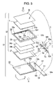
- FIG. 5 is an exploded perspective view showing another embodiment of the electro-optical device according to the invention.
- FIG. 6 is a cross-sectional side view showing the disassembled electro-optical device of FIG. 5 .
- FIG. 7 is a plan view showing the main part of the FPC board from the arrow B direction of FIG. 6 .
- FIG. 7A is a plan view showing the relation of hole and pin
- FIG. 7B is an enlarged plan view showing the part indicated by the arrow I of FIG. 7A .
- FIG. 8 is a view showing another embodiment of the shape of hole and projecting part.
- FIG. 9 is a view showing a further embodiment of the shape of hole and projecting part.
- FIG. 10 is a view showing another embodiment of the shape of pin.
- FIG. 11 is a block diagram showing an embodiment of the electronic apparatus according to the invention.
- FIG. 12 is a perspective view showing another embodiment of the electronic apparatus according to the invention.
- FIG. 1 illustrates the embodiment of the liquid crystal display device as the lighting device and electro-optical device using the lighting device in the disassembly state.
- FIG. 2 shows the cross section structure of the side part in assembling the liquid crystal display device in FIG. 1 .
- the lighting device according to the embodiment for example, is the lighting device with the configuration used as the edge light-type backlight for the electro-optical device called the liquid crystal display device.
- the lighting device 2 is the lighting device of the configuration using the plurality of LEDs (Light Emitting Diodes) which are punctate light sources as the light source.
- LEDs Light Emitting Diodes
- the liquid crystal display device 1 includes the liquid crystal panel 3 as the electro-optical panel, FPC (Flexible Printed Circuit) as the wiring board 4 , the lighting device 2 and the case 5 .
- the side marked the arrow A is the observation part.
- the liquid crystal panel 3 is formed by joining the first substrate 11 and the second substrate 12 faced with it by using the sealant 13 of the square or rectangle frame shape from the view of the observation direction of the arrow A.
- the sealant 13 of the square or rectangle frame shape from the view of the observation direction of the arrow A.
- the first substrate 11 has the first translucent substrate 11 a of the square or rectangle form from the view of the observation direction indicated by the arrow A.
- the first translucent substrate 11 a for example, is formed by translucent glass, translucent plastic and the like.
- the polarizing plate 15 a is mounted on the external surface of the first translucent substrate 11 a through the adhesion and so on. It is preferable to use other suitable optical components if necessary.
- the second substrate 12 opposite to the first substrate 11 has the second translucent substrate 12 a of the square or rectangle form from the view of the observation direction indicated by the arrow A.
- the second translucent substrate 12 a for example, is formed by translucent glass, translucent plastic and the like.
- the polarizing plate 15 b is mounted on the external surface of the second translucent substrate 12 a through the adhesion and so on. It is preferable to use other suitable optical components if necessary.
- the liquid crystal panel 3 can be configured by optional display mode.
- any one of the simple matrix mode and the active matrix mode will be good.
- TN Transmission Nematic
- STN Super Twisted Nematic
- the vertical orientation mode completed from the liquid crystal with the sub-permittivity and other optional liquid crystal may be utilized.
- any one of translucent mode, reflection mode and semi-translucent mode will be good.
- the translucent mode or the semi-translucent mode will be good as the lighting.
- the simple matrix mode is the matrices mode to which a driving signal is directly applied when each pixel does not have the active element and the intersection part corresponds to pixel or dot.
- TN and STN are used as the liquid crystal mode for the mode.
- the active matrix is the matrices mode in which the active elements are provided for each pixel or dot, the power voltage is written when the active element is ON during the reading and the power voltage is preserved and maintained when the active element is OFF in other period.
- 3-terminal type and 2-terminal type as the active element used in this mode.
- TFT Thin Film Transistor
- TFD Thin Film Diode
- the color filter is provided on the first substrate 11 and the second substrate 12 .
- the color filter selectively transmits the light in the specific wavelength band. Specifically, by corresponding each color of 3 primary colors such as B (blue), G (green) and R (red) to each dot on the first substrate 11 or the second substrate 12 , predetermined arrangements such as stripe arrangement, delta arrangement and mosaic arrangement are lined up.
- the second translucent substrate 12 a constituting the second substrate 12 in FIG. 2 includes the flared portion 21 attached to the external side of the first substrate 11 , the opposed board.
- the driving IC 22 for driving the liquid crystal panel 3 for example, is mounted on the surface of the first substrate 11 part of the flared portion 21 by means of COG (Chip On Glass) using ACF (Anisotropic Conductive Film) 23 . As shown in FIGS. 1 , 3 driving ICs 22 are mounted in the embodiment.
- the driving IC 22 drives the liquid crystal panel 3 by outputting the scan signal and data signal to the electrode of the liquid crystal panel 3 .
- the wiring 24 on the end side of the second translucent substrate 12 a contacted on the flared portion 21 are formed the wiring 24 .
- the wiring 24 of which plural lines open the gap toward the vertical direction from the ground each other is formed.
- the wiring 24 is connected to the output terminal of the driving IC 22 such as the output bump.
- the wiring 24 extends the inside of the liquid crystal panel 3 , that is, the liquid crystal layer 14 (See FIG. 1 .), so it is connected to the scan electrode and the data electrode in case of the simple matrix mode.
- the wiring 24 is connected to the active element and electrode such as TFD element or TFT element in the active matrix.
- the external connection terminal 25 is formed in the flared portion 21 .
- the external connection terminal 25 is connected to the input terminal of the driving IC 22 such as the input bump.
- the external connection board 25 for example, is connected to the FPC board 4 , the wiring board having the flexibility by ACF 23 .
- the conductive connection techniques such as soldering, heat seal and the like are used for the connection of the FPC board 4 and the external connection terminal 25 .
- the FPC board 4 is the board with excellent bendability using the film made of polyimide or polyester as material.
- the FPC board 4 comprises the surface S 1 facing the liquid crystal panel 3 and its opposed surface S 2 since it can be bended as shown in the arrow C of FIG. 1 .
- the surface S 1 can be contracted owing to bendability, while the surface S 2 can be extended owing to bendability.
- FPC board 4 comprises the input terminal 4 a , the bending part 4 b and the output terminal 4 c.
- the bending part 4 b is the part bended in bending the FPC board 4 like the arrow C.
- the input terminal 4 a is connected to the control circuit, the power source and the like such as cellular phone, personal digital assistant and the like.
- the FPC board 4 are formed a plurality of circuit parts required for driving the liquid crystal panel 3 and a plurality of wirings constituting the circuit through the connection of the plurality of circuit parts.
- the graphic display of the circuit parts and the wirings is omitted.
- the plurality of circuit parts are vertically arranged in parallel to the end side of the liquid crystal panel 3 that is, the end side of the second substrate.
- the bending part 4 b is extended and a plurality of wirings 27 which is extended toward the liquid crystal panel 3 is provided on the side surface S 2 .
- the wiring 27 is extended toward the direction vertical to the end side of the second substrate 12 , that is, the end side of the liquid crystal panel 3 .
- the wiring 27 transmits the output signal of the electronic circuit formed by a plurality of circuit parts to the output terminal 4 c.
- the signal transmitted to the output terminal 4 c is transmitted to the driving IC 22 via the external connection terminal 25 of the liquid crystal panel 3 .
- the lighting device 2 comprises the light guide 7 , LED 6 (mounted on the FPC board 4 ) as the light source and a plurality of optical sheets 33 , 34 a and 34 b .
- the light guide 7 is placed on the second substrate 12 side of the liquid crystal panel 3 .
- the light guide 7 for example, is formed by translucent resin.
- the later side 7 a opposite to the flared portion 21 is the light receiving plane.
- the lateral plane on which the arrow A, that is, the plane opposite to the liquid crystal panel 3 is 7 b the light transmitting plane.
- a plurality of convex portions 35 on the sides positioned on both sides of the light receiving plane 7 a are provided a plurality of convex portions 35 .
- four convex portions 35 on one side that is to say, total eight convex portions on both sides are provided.
- Four convex portions 35 have two convex portions 35 a provided on the light transmitting plane 7 b side and two convex portions 35 b provided on its opposite side.
- the convex portion 35 a prevents the light guide 7 received in the case 5 from moving toward the indicating direction of the arrow B.
- the convex portion 35 b prohibits the light guide 7 received in the case 5 from moving toward the indicating direction of the arrow A.
- LED 6 is shown at the position close to the bending part 4 b on the surface S 1 of the FPC board 4 and is evenly arranged in parallel to the end side of the first substrate 11 , that is, the end side of the liquid crystal panel 3 .
- the emitting plane 6 a of LED 6 faces toward the direction opposite to the end side of the first substrate 11 .
- three LEDs 6 are provided at a predetermined interval, for example, at even intervals. In a condition that the FPC board 4 is bended toward the direction of arrow C as shown in FIG. 2 , three LEDs 6 are arranged so that the emitting plane 6 a is opposed to the light receiving plane 7 a of the light guide 7 .
- the light generated from LED 6 is introduced into the inside of the light guide 7 through the light receiving plane 7 a , passes through the inside and is emitted from the light transmitting plane 7 b as the light on the flat plane.
- the light source may be constituted by the punctate light source excepting LED 6 or the linear light source called the cold-cathode tube.
- FIG. 1 on the reverse side of the light guide 7 in relation to the direction of the arrow A is provided that light reflecting layer 36 if necessary.
- the light transmitting plane 7 b is provided a plurality of optical sheets if necessary.
- one light diffusion sheet 33 and two prism sheets 34 a and 34 b are provided as a plurality of optical sheets.
- the prism sheet is one. If necessary, other optical sheets excepting such optical sheets may be used.
- the light diffusion sheet 33 is provided so as to be contacted with the light transmitting plane 7 b of the light guide 7 , specifically, with the sheet of the light transmitting plane 7 b.
- the light diffusion sheet 33 can diffuse the light emitted from the light transmitting plane 7 b.
- the diffused light is emitted to the outside of the light device 2 as the even light of the sheet spread throughout the light transmitting plane 7 b.
- the prism sheets 34 a and 34 b are provided on the light diffusion sheet 33 as shown in FIG. 2 .
- These prism sheets 34 a and 34 b are the optical components used to focus the incident light toward a specific direction, that is to say, they are formed by arranging a plurality of prism figures in parallel to each other.
- 2 prism sheets 34 a and 34 b are successively established. These, for example, are arranged so that the arrangement direction of the prism figures is at right angles to each other. Using these prism sheets 34 a and 34 b can raise the strength by focusing the light headed toward the liquid crystal panel 3 .
- the part constituted by the LED 6 , light guide 7 , light reflecting layer 36 , light diffusion sheet 33 , and 2 prism sheets 34 a and 34 b is the lighting device 2 .
- the light is transmitted to the liquid crystal panel 3 by the lighting device 2 .
- a light blocking sheet 37 formed by the light blocking material is provided between the above-mentioned prism sheets 34 a and 34 b , and the liquid crystal panel 3 .
- the light blocking sheet 37 has a light blocking portion 37 a and an opening portion 37 b , as shown in FIG. 1 .
- the opening portion 37 b of the light blocking sheet 37 the light emitted from the light transmitting plane 7 b of the light guide 7 passes through and is transmitted to V range, the display of the liquid crystal panel 3 .
- the light blocking portion 37 a the light emitted from the light guide 7 is blocked, so that the light emitted from the range except for the display area V of the liquid crystal panel 3 is prevented to come through.
- the light blocking sheet 37 has the adherence on both portions.
- the adherence means the adherent capable of easily scrubbing by hand.
- the liquid crystal panel 3 is adhered to the case 5 by the light blocking sheet 37 .
- the case 5 comprises the light guide receiving part 5 a , the liquid crystal panel receiving part 5 b , the light guide latching part 5 c and LED receiving part 5 d .
- the case 5 for example, can be formed by resin materials such as plastic, etc.
- the light guide receiving part 5 a is shown in the inside of the case 5 , as shown in FIG. 2 , is provided on the side in which the arrow B is marked, and accepts the light guide 7 .
- the liquid crystal panel receiving part 5 b is shown in the side of the case 5 , is provided on the observation side in which the arrow A is marked, and accepts the liquid crystal panel 3 .
- the light guide latching part 5 c is provided on both sides inside the light receiving part 5 a.
- 8 light guide latching parts 5 c are provided. If the convex portion 35 a and 35 b of the light guide are fitted to the light guide latching part 5 c , the light guide 7 is fixed in the case 5 .
- LED receiving part 5 d in which the light guide 7 is contained in the light guide receiving part 5 a is provided between the light receiving plane 7 a of the light guide 7 and the case 5 , and contains LED 6 in a condition of bending the FPC board 4 to the arrow C.
- the driving IC 22 When assembling the liquid crystal display device 1 shown in FIG. 2 by using the liquid crystal panel 3 , the driving IC 22 , the FPC board 4 and the lighting device 2 shown in FIG. 1 , first, mount the driving IC 22 in the flared portion 21 of the liquid crystal panel 3 and install the polarizing plates 15 a and 15 b in FIG. 2 in the liquid crystal panel 3 . Next, connect the FPC board 4 to the part establishing the external terminal 24 in the flared portion 21 of the liquid crystal panel 3 . Next, put the lighting device 2 of FIG. 1 into the light guide receiving part 5 a of the case 5 .
- the lighting device 2 in which total eight convex portions 35 a and 35 b provided in the light guide 7 are inserted into the light guide latching part 5 c of the case 5 , respectively, is positioned so as not to be dislocated in the case 5 .
- the light blocking sheet 37 is provided between the liquid crystal panel receiving part 5 b and the end side of the prism sheet 34 b , and attaches both parts. And, put the liquid crystal panel 3 into the liquid crystal panel receiving part 5 b . The receiving liquid crystal panel 3 is adhered to the case 5 by the light blocking sheet 37 . Therefore, the lighting device of the liquid crystal panel 3 the lighting device is positioned at a fixed position within the case 5 by restraining from being positioned in the left-right direction and the direction vertical to the ground as shown in FIG. 2 by the case 5 . Next, bend the FPC board 4 like the arrow C of FIG. 1 and in FIG.
- the liquid crystal panel 3 , the lighting device 2 and the FPC board 4 are received in the case 5 according a predetermined positioning relation, and then, the liquid crystal display device is manufactured.
- FIG. 3A shows the FPC board 4 and the case 5 located around the part connecting the FPC board 4 to the liquid crystal panel 3 in the liquid crystal display device 1 shown in FIG. 1 .
- FIG. 3B shows the enlarged part indicated by the symbol IIIB in FIG. 3A .
- the hole 42 a in which the pin 41 a is inserted is a little larger than the diameter of the pin 41 a formed in the cylinder figure, and specifically, the hole 42 a is formed so large as the pin 41 a cannot be move within the hole over the allowable limit size.
- the allowable limit size is the size set so as to show the expected capability of the lighting device 2 . For example, there can be provided the setting range of LED 6 considered in order to transmit the light emitted from LED 6 to the light guide 7 in the sufficient intensity.
- the hole 42 a when the liquid crystal display device 1 is assembled as shown in FIG. 2 , is a positioning hole executing the positioning of LED 6 in parallel direction, namely Y-direction, with the light receiving plane 7 a of the light guide 7 .
- FIG. 3A by using the result that the pin 41 a is inserted into the positioning hole 42 a , the position of Y-direction of the FPC board 4 can be determined when the liquid crystal display device 1 is assembled. According to this, the LED 6 mounted on the FPC board 4 can determine the Y-directional position for light receiving plane 7 a.
- both the pin 41 a and the hole 42 a are formed on a circular form, the hole 42 a executes the positioning of pin 41 a for X-direction and the other whole area of 360° direction without the limitation of Y-direction.
- the projecting part 43 protruded inside the hole 42 b from a periphery 43 a of the hole 42 b is provided.
- the projecting part 43 is formed simultaneously together with the hole 42 b by forming the hole 42 b on the shape including the projecting part 43 on the FPC board 4 . Therefore, the projecting part 43 has flexibility and elasticity as the FPC board 4 .
- Elasticity is a property that an object deformed by an external force returns to the original state when the external force is removed. That is, the projecting part 43 with elasticity has a repulsive power recovering the original state if it can be bent by the external force.
- FIG. 4 shows the enlarged state that the pin 41 b is inserted into the hole 42 b in FIG. 2 .
- FIG. 4A is a plan view taken from the arrow B direction of FIG. 2 .
- FIG. 4B is a cross-sectional view of FIG. 4A along IVB-IVB line.
- the Y-directional width w 1 of the hole 42 b is sufficiently larger than the diameter d 1 of pin 41 b, specifically, the distance between the pin 41 a and the hole 42 a.
- the Y-directional position of LED 6 is determined by using the result that the pin 41 a is inserted into the positioning hole 42 a. At this time, it is considered that the size difference occurs in the distance t 1 between the pin 41 a and the pin 41 b , and the distance t 2 between the positioning hole 42 a and the hole 42 b , or the disparity occurs in the assembly of members as liquid crystal panel 3 or FPC board 4 , etc. As shown in FIG.
- the projecting part 43 is protruded straightly inside the first hole, the width w 2 between the front end of the projecting part 43 and the periphery of the hole 42 b is formed smaller than the diameter d 1 of the pin 41 b .
- the projecting part 43 of FIG. 4B is pressed so as to rotate round the upward direction of paper, that is, Y-direction.
- the FPC board 4 is pushed toward the direction of arrow G which is the reverse X-direction. That is, in FIG. 2 , the FPC board 4 is pushed toward the light receiving plane 7 a of the light guide 7 so as to move.
- the emitting plane 6 a of LED 6 is provided in the position close to the light receiving plane 7 a of the light guide 7 . It is more preferable that the emitting plane 6 a is provided so as to be contacted with the light receiving plane 7 a , that is, the gap is zero. In this case, since the light emitted from LED 6 is introduced directly into an internal part of the light guide 7 from the light receiving plane 7 a , the light can be used efficiently without lowering the brightness of the light.
- the gap occurs between LED 6 and the light guide 7 after it is assembled if the consideration is not made for the FPC board 4 and the light guide 7 , since it is necessary to consider the disparity when LED 6 is mounted on the FPC board 4 and the tolerance for assembling in case that the liquid crystal display device 1 is assembled.
- the brightness of the light introduced into the light guide 7 is lowered.
- the gap of 0.1 mm occurs between the light receiving plane 7 a and the emitting plane 6 a
- the brightness of the light introduced into the light guide is lowered by approximately 10%.
- the disparity occurs in the brightness of the light introduced into the light guide 7 since the disparity occurs in the position of LED 6 for the light guide 7 .
- the LED 6 mounted on the FPC board 4 can approach and contact the light receiving plane 7 a of the light guide 7 . According to this, the light emitted from LED 6 is efficiently introduced into the internal part of the light guide 7 without lowering brightness. As a result, the brightness of the light emitted from the light guide 7 can be raised. Moreover, since the emitting plane 6 a of LED 6 is contacted with the light receiving plane 7 a of the light guide 7 , it is prevented that the position of LED 6 for the light guide 7 is dispersed. As a result, it is prevented that disparity occurs the brightness of the light introduced into the light guide 7 .
- FIG. 5 shows another embodiment according to the lighting device and the electro-optical device of the invention.
- FIG. 6 shows the cross-sectional side structure when the liquid crystal display device of FIG. 5 is assembled.
- the liquid crystal display device 1 corresponding to the previous embodiment shown in FIG. 1 , there is employed the structure in which the LED 6 as a light source is mounted on the FPC board 4 connected with the liquid crystal panel 3 .
- the liquid crystal display device 51 shown in FIG. 5 employs the structure that provides a LED board 58 in addition to the FPC board 54 connected to the liquid crystal panel 53 and mounts the LED 6 on the LED board 58 .
- the liquid crystal display device 51 of FIG. 5 will be described from a different standpoint from the liquid crystal display device 1 of FIG. 1 .
- the element as same as the embodiment of FIG. 1 is given the same symbol, and the description is omitted.
- the constitution of the liquid crystal display device 51 shown in FIG. 5 can be same as the liquid crystal display device 1 shown in FIG. 2 except the FPC board 54 and the LED board 58 .
- the shape of the case 55 adjacent to the part mounting the LED board 58 is different.
- the liquid crystal panel 53 can be configured identically as the liquid crystal panel 3 of FIG. 1 .
- the FPC board 54 as a wiring board is connected with the end of the flared portion 21 of the liquid crystal panel 53 , for example, through ACF 23 .
- the FPC board 54 has the surface S 1 bent as the arrow C of FIG. 5 and opposite to the liquid crystal panel 53 , and the surface S 2 on the opposite side of S 1 .
- the FPC board 54 has a input terminal 54 a , a bending part 54 b , a output terminal 54 c , a LED terminal 54 d .
- the FPC board 54 can be configured as same as the FPC board of FIG. 1 except for the following points.
- the FPC board 4 mounts three LEDS 6 on the surface S 1 of the shrunken side
- the FPC board 54 of FIG. 5 does not mount the LED 6 .
- the hole 42 a and 42 b are provided in the both ends adjacent to the bending part 4 b , but in the FPC board 54 of FIG. 5 , these holes 42 a and 42 b are not provided.
- the LED terminal 54 d is provided on the surface S 1 of the shrunken side of the FPC board 54 .
- the LED terminal 54 d is connected electrically to the input terminal 58 a of the LED board 58 described below, for example, with the solder, etc.
- both LED terminals can be connected through the connector.
- the case 55 has the light guide receiving part 55 a , the liquid crystal panel receiving part 55 b , the light guide latching part 55 c and the LED receiving part 55 d , and is formed by using resin such as plastic, etc.
- this case 55 can be the same structure as the case 5 of FIG. 1 , it is different in the following points.
- the pin 41 a and the pin 41 b are provided respectively in both corners where the light receiving plane 7 a is located.
- the pin 61 a as the second protrusion and the pin 61 b as the first protrusion are provided respectively in both corners where the light receiving plane 7 a is located.
- These pin 61 a and 61 b are formed in the cylinder figure protruded from the side marked the arrow A of the case 55 .
- the lighting device 52 has the light guide 7 , the LED 6 as a light source, the plurality of optical sheets 33 , 34 and 34 b , and the LED board 58 mounting the LED 6 .
- the lighting device 52 is configured as same as the lighting device 2 of FIG. 1 except the LED board 58 .
- the LED board 58 shown in FIG. 5 is an excellent bendable board formed with films such as polyimide, polyester, etc. as a base material.
- the input terminal 58 a is provided in the end of the bending part 58 b of the LED board 58 . As described above, the input terminal 58 a is connected with the LED terminal 54 d of the FPC board 54 .
- the bending part 58 b of the LED board 58 can be bent in the state that it is connected with the FPC board 54 which can be bent as the arrow C of FIG. 5 .
- the plurality of LEDs 6 are mounted on the surface S 3 of the LED board 58 .
- the two holes 62 a , 62 b are provided in the LED board 58 . These holes 62 a and 62 b , when the liquid crystal display device 51 is assembled, are provided in the position where he pin 61 a and 62 b are inserted into the hole 62 a and 62 b , respectively.
- FIG. 7A shows the LED board 58 and the case 55 of the liquid crystal display device 51 shown in FIG. 5 from the side marked the arrow B.
- FIG. 7B shows the enlarged part indicated by the symbol I in FIG. 7A .
- the hole 62 a in which the pin 61 a is inserted is slightly larger than the diameter of the pin 61 a , specifically, the pin 61 a is formed slightly large so as to move in the hole 62 a within allowable limit size.
- the hole 62 a when the liquid crystal display device 51 is assembled as FIG. 6 , is a positioning hole executing the positioning of LED 6 in parallel direction, namely Y-direction, with the light receiving plane 7 a of the light guide 7 .
- FIG. 6 shows the LED board 58 and the case 55 of the liquid crystal display device 51 shown in FIG. 5 from the side marked the arrow B.
- FIG. 7B shows the enlarged part indicated by the symbol I in FIG. 7A .
- the Y-directional position of the LED board 58 can be determined when the liquid crystal display device 51 is assembled. According to this, the LED 6 mounted on the LED board 58 can determine the Y-direction position for the light receiving plane 7 a.
- the projecting part 63 protrudes inside the hole 62 b from a periphery 63 a of the hole 62 b is provided.
- the projecting part 63 is formed simultaneously together with the hole 62 b by forming the hole 62 b on the shape including the projecting part 63 on the LED board 58 . Therefore, the projecting part 63 has flexibility and elasticity as the LED board 58 .
- the projecting part 63 with elasticity has a repulsive power recovering the original state if it can be bent by the external force.
- the Y-directional width w 1 of the hole 62 b is formed larger than the diameter d 1 of the pin 61 b .
- the Y-directional position of LED 6 is determined by using the result that the pin 61 a is inserted into the positioning hole 62 a .
- the size difference occurs in the distance t 1 between the pin 61 a and the pin 61 b , and the distance t 2 between the positioning hole 62 a and the hole 62 b , or that the disparity occurs in the assembly of the members.
- FIG. 7A the Y-directional position of LED 6 is determined by using the result that the pin 61 a is inserted into the positioning hole 62 a .
- the width w 2 between the head of the projecting part 63 and the end of the hole 62 b is formed to be narrower than the diameter d 1 of the pin 61 b .
- the LED board 58 is pushed toward the direction of arrow G in the reverse direction to X. That is, in FIG. 6 the LED board 58 is pushed to move toward the light receiving plane 7 a of the light guide 7 .
- the projecting part 63 presses the pin 61 b so that the LED board 58 moves toward the light receiving plane 7 a of the light guide 7 , and thereby the LED 6 provided on the LED board 58 contacts closely with the light receiving plane 7 a of the light guide 7 .
- the light emitted by the LED 6 is effectively introduced inside the light guide 7 without lowering of the brightness. Therefore, the brightness of the light emitted from the light guide 7 can be raised.
- the light emitting plane 6 a of the LED 6 contacts with the light receiving 7 a of the light guide 7 , and thereby the disparity of the positions of the LED 6 for the light guide 7 can be provided to occur. Therefore, the disparity of the light introduced inside the light guide 7 can be prevented to occur.
- the hole 42 b , 62 b is larger in the Y direction than the diameter d 1 of the pin 41 b , 61 b and thus has margin thereof in the direction, that is, more specifically, the hole 42 b , 62 b is formed to be a rectangle whose distance to the pin 41 b , 61 b is sufficiently larger than the distance between the pin 41 a , 61 a and the hole 42 a , 62 a.
- the projecting part 43 , 63 is formed to extend toward the X direction approximately in the middle of the long side extending toward the Y direction of the hole 42 b , 62 b.
- the shape of the hole 42 b , 62 b and the projecting part 43 , 63 is not limited to the above-referenced shapes.
- the shape of the hole 42 b , 62 b may have an elliptical shape.
- the hole 42 b , 62 b is formed to have its long axis extending toward the Y direction, that is, the parallel direction to the light receiving plane 7 a in FIG. 1 or FIG. 5 .
- the projecting part 43 , 63 is formed to extend toward the center of the ellipse from the periphery 43 a , 63 a of the ellipse toward the X direction, that is, toward the short axis direction.
- the projecting part 43 , 63 is formed so that the width of the projecting part 43 , 63 gets smaller in steps toward the X direction in the same elliptical hole 42 b , 62 b as FIG. 8A .
- the width of the projecting part 43 , 63 vary in steps as above, the forces F (cf. FIG. 4B ) with which the projecting part 43 , 63 presses the pin 41 b , 61 b can be adjusted.
- the hole in case that the projecting part is formed in steps is not limited to elliptical shapes and others.
- the projecting part 43 , 63 is formed on both the edges distant from the center of the long side of the same rectangular hole 42 b , 62 b as FIG. 4B , and the pin 41 b , 61 b is pressed by the projecting part 43 , 63 on both the edges.
- the projecting part 43 , 63 is formed on one side distant from the center of the long side of the same rectangular hole 42 b , 62 b.
- the pin 41 a , 41 b , 61 a , 61 b is formed to be in a cylinder shape protruding through the case 5 , 55 .
- the shape of the pin 41 a , 41 b , 61 a , 61 b is not limited to the above.
- the cross-sectional shape is at one's discretion and may be round, elliptical, rectangular, square, and so on, for instance.
- the head of columnar pin 41 a , 41 b , 61 a , 61 b may be formed to be round.
- the pin 41 a , 41 b , 61 a , 61 b can easily protrude into the positioning hole 41 a , 61 a and the hole 41 b , 61 b, making easy the assembling of the liquid crystal display device 1 in FIG. 1 and the liquid crystal display device 51 in FIG. 5 .
- the head of the pin 41 a , 41 b , 61 a , 61 b is in a bended shape and is formed to be in a hook shape from a lateral view.
- the pin 41 a , 41 b , 61 a , 61 b becomes hard to drop out of the positioning hole 41 a , 61 a and the hole 41 b , 61 b , preventing the displacement of the LED 6 caused by sliding of the board when the liquid crystal display device 1 in FIG. 1 or the liquid crystal display device 51 in FIG. 5 is given an impact.
- FIG. 11 shows an embodiment of the electronic apparatus according to the invention.
- the electronic apparatus shown herein comprises the liquid crystal display device 111 and the control circuit 110 for controlling it.
- the control circuit 110 is constituted by the display information processing circuit 115 , the power supply circuit 116 , the timing generator 117 , and the display information output source 118 .
- the liquid crystal display device 111 has the liquid crystal panel 113 , the lighting device 112 , and the driving circuit 114 .
- the display information output source 118 comprises pieces of memory such as a RAM (Random Access Memory) and the like, storage units such as various types of disks and so forth, tuning circuit synchronously outputting digital image signals and so on, and provides the display information circuit 115 for the display information such as image signals with predetermined format, etc. based on a variety of clock signals generated in the timing generator 117 .
- RAM Random Access Memory
- storage units such as various types of disks and so forth
- tuning circuit synchronously outputting digital image signals and so on
- the display information circuit 115 for the display information such as image signals with predetermined format, etc. based on a variety of clock signals generated in the timing generator 117 .
- the display information processing circuit 115 comprises a number of known circuits such as an amplifying and inverting circuit, a rotation circuit, a gamma-correction circuit, a clamping circuit and so on, and performs processing of inputted display information and then provides the driving circuit 114 with image signals together with clock signal CLK.
- the driving circuit 114 herein is a generic term used to refer to a scan line driving circuit, a data line driving circuit, and further inspecting circuit, etc.
- the power supply circuit 116 provides each of the above-referenced components with predetermined power supply voltage.
- the liquid crystal display device 111 may be constituted using the liquid crystal display device 1 shown in FIG. 1 or the liquid crystal display device 51 shown in FIG. 5 .
- the liquid crystal display device 1 , 51 can perform the bright display without disparity since the liquid crystal display device 1 , 51 uses the lighting device 2 , 52 which emits the light with high brightness and without instability. Therefore, the electronic apparatus according to the invention using the liquid crystal display device 1 , 51 can display information related to the electronic apparatus with stability and brightness.
- FIG. 12 shows a cellular phone which is another embodiment of the electronic apparatus according to the invention.
- the cellular phone 120 shown herein has the body 121 and the display part 122 provided on the body 121 to be able to open and shut.
- the display device 123 composed of electro-optical devices such as a liquid crystal display device and the rest is placed in the display part 122 , and each indication regarding telephone communication is visible in the display screen 124 of the display part 122 .
- the operating button 125 is arranged on the body 121 .
- the antenna 126 is provided to be retractable.
- a speaker which is not illustrated, is placed in the receiving part 127 .
- a microphone which is not illustrated as well, is embedded in the transmitting part 128 provided at the bottom of the body 121 .
- the control unit for controlling the operation of the display device 123 is contained as a part of the control unit generally controlling the cellular phone, otherwise in the body 121 or the display part 122 separately from the control unit.
- the display device 123 may be constituted, for example, using the liquid crystal display device 1 shown in FIG. 1 or the liquid crystal display device 51 shown in FIG. 5 .
- the liquid crystal display device 1 , 51 can perform the bright display without disparity due to the use of the lighting device 2 , 52 emitting light with high brightness and no disparity. Therefore, the cellular-phone 120 according to the invention using the liquid crystal display device 1 , 51 can display information related to the cellular phone 120 with stability and brightness.
Landscapes
- Physics & Mathematics (AREA)
- General Physics & Mathematics (AREA)
- Optics & Photonics (AREA)
- Liquid Crystal (AREA)
- Planar Illumination Modules (AREA)
- Devices For Indicating Variable Information By Combining Individual Elements (AREA)
Abstract
Description
Claims (11)
Applications Claiming Priority (2)
| Application Number | Priority Date | Filing Date | Title |
|---|---|---|---|
| JP2005-063479 | 2005-03-08 | ||
| JP2005063479A JP4244942B2 (en) | 2005-03-08 | 2005-03-08 | Liquid crystal device, lighting device, and electronic device |
Publications (2)
| Publication Number | Publication Date |
|---|---|
| US20060203515A1 US20060203515A1 (en) | 2006-09-14 |
| US7490973B2 true US7490973B2 (en) | 2009-02-17 |
Family
ID=36970668
Family Applications (1)
| Application Number | Title | Priority Date | Filing Date |
|---|---|---|---|
| US11/348,439 Active 2026-09-02 US7490973B2 (en) | 2005-03-08 | 2006-02-06 | Lighting device, electro-optical device and electronic apparatus |
Country Status (4)
| Country | Link |
|---|---|
| US (1) | US7490973B2 (en) |
| JP (1) | JP4244942B2 (en) |
| KR (1) | KR100764254B1 (en) |
| CN (1) | CN100388091C (en) |
Cited By (9)
| Publication number | Priority date | Publication date | Assignee | Title |
|---|---|---|---|---|
| US20080024697A1 (en) * | 2006-07-31 | 2008-01-31 | Wal-Hee Kim | Flexible printed circuit, back light assembly, and liquid crystal display including the same |
| US20080094535A1 (en) * | 2006-10-18 | 2008-04-24 | Samsung Electronics Co., Ltd. | Backlight assembly and display apparatus having the same |
| US20090059129A1 (en) * | 2007-08-31 | 2009-03-05 | Innocom Technology(Shenzhen) Co., Ltd. | Light source assembly and liquid crystal display utilizing the same |
| US20100296310A1 (en) * | 2009-05-25 | 2010-11-25 | Samsung Electronics Co., Ltd. | Backlight unit of display apparatus |
| US20110149602A1 (en) * | 2009-12-22 | 2011-06-23 | Lg Innotek Co., Ltd. | Backlight unit |
| US20110157519A1 (en) * | 2009-12-28 | 2011-06-30 | Casio Computer Co., Ltd. | Light source apparatus and display apparatus using light source apparatus |
| US20120087110A1 (en) * | 2009-06-24 | 2012-04-12 | Lpoint Co., Ltd. | Device for coupling module circuit board and frame and backlight using the same |
| US20120287670A1 (en) * | 2010-04-09 | 2012-11-15 | Sharp Kabushiki Kaisha | Light source module and electronic apparatus provided with same |
| US20120320630A1 (en) * | 2010-03-31 | 2012-12-20 | Sharp Kabushiki Kaisha | Illumination apparatus and display device |
Families Citing this family (22)
| Publication number | Priority date | Publication date | Assignee | Title |
|---|---|---|---|---|
| KR101320893B1 (en) * | 2007-02-14 | 2013-10-22 | 삼성디스플레이 주식회사 | Backlight assembly and display device having the same |
| CA2653169A1 (en) * | 2007-03-30 | 2008-10-09 | Hitachi Chemical Co., Ltd. | Optical connecting member and display apparatus |
| JP4650448B2 (en) * | 2007-04-03 | 2011-03-16 | 豊田合成株式会社 | Backlight device |
| BRPI0915733A2 (en) * | 2008-07-08 | 2015-10-27 | Sharp Kk | liquid crystal video device |
| JP5072823B2 (en) * | 2008-12-25 | 2012-11-14 | 株式会社ジャパンディスプレイセントラル | Backlight unit and liquid crystal display device |
| US20120257107A1 (en) * | 2009-12-28 | 2012-10-11 | Sharp Kabushiki Kaisha | Illumination device, liquid crystal display device and television receiver device |
| US8979293B2 (en) * | 2010-09-24 | 2015-03-17 | Sharp Kabushiki Kaisha | Lighting device, display device, and television device |
| WO2012132147A1 (en) * | 2011-03-28 | 2012-10-04 | 株式会社村田製作所 | Electronic part and method for producing same |
| CN102999226A (en) * | 2011-09-12 | 2013-03-27 | 宸鸿科技(厦门)有限公司 | Reflection-type touch display device and manufacturing method thereof |
| CN105122126A (en) * | 2013-04-18 | 2015-12-02 | 夏普株式会社 | Display device |
| KR101351880B1 (en) * | 2013-07-19 | 2014-01-17 | 삼성디스플레이 주식회사 | Back-light assembly and display apparatus having the same |
| KR102090200B1 (en) * | 2013-08-08 | 2020-03-18 | 삼성디스플레이 주식회사 | Organic light emitting diode display |
| CN104637927B (en) * | 2013-11-12 | 2019-01-22 | 中国科学院微电子研究所 | Three-dimensional packaging structure based on flexible substrate and process method |
| US9841645B2 (en) | 2015-04-02 | 2017-12-12 | Himax Display, Inc. | Display device |
| CN104765175A (en) * | 2015-04-13 | 2015-07-08 | 业成光电(深圳)有限公司 | Panel assembly |
| JP6050856B2 (en) * | 2015-04-21 | 2016-12-21 | 立景光電股▲ふん▼有限公司 | Display panel |
| CN106200166A (en) * | 2016-08-22 | 2016-12-07 | 青岛海信电器股份有限公司 | A kind of liquid crystal module and liquid crystal indicator |
| JP2019192574A (en) * | 2018-04-27 | 2019-10-31 | シャープ株式会社 | Composite light guide member, lighting device, and display device |
| JP6790035B2 (en) * | 2018-09-19 | 2020-11-25 | ミネベアミツミ株式会社 | Planar lighting device |
| CN109870850B (en) * | 2019-03-27 | 2021-02-26 | 武汉华星光电技术有限公司 | Backlight module and liquid crystal display |
| CN110058455B (en) * | 2019-04-29 | 2021-09-24 | 厦门天马微电子有限公司 | Backlight module and display device |
| KR102216332B1 (en) * | 2019-07-24 | 2021-02-16 | 세메스 주식회사 | A unit for checking the discharge state of chemical liquid |
Citations (10)
| Publication number | Priority date | Publication date | Assignee | Title |
|---|---|---|---|---|
| US3731077A (en) * | 1971-03-31 | 1973-05-01 | Honeywell Inc | Illuminated indicator for high and low ambient light environments |
| US4729185A (en) * | 1985-01-30 | 1988-03-08 | Kabushiki Kaisha Toshiba | Display panel illumination device |
| JPH1039779A (en) | 1996-07-24 | 1998-02-13 | Toshiba Electron Eng Corp | Plane display device |
| JP2000147544A (en) | 1998-11-12 | 2000-05-26 | Matsushita Electric Ind Co Ltd | Liquid crystal display device fitting/connecting device |
| JP2001330830A (en) | 2000-05-23 | 2001-11-30 | Seiko Epson Corp | Liquid crystal device and electronic equipment |
| JP2002100228A (en) | 2000-09-21 | 2002-04-05 | Sanyo Electric Co Ltd | Surface illuminating apparatus |
| JP2004177876A (en) | 2002-11-29 | 2004-06-24 | Optrex Corp | Liquid crystal display |
| JP2004184493A (en) | 2002-11-29 | 2004-07-02 | Seiko Epson Corp | Electrooptical device, method for manufacturing electrooptical device, and electronic equipment |
| JP2004258236A (en) | 2003-02-25 | 2004-09-16 | Seiko Epson Corp | Electro-optical device and electronic device |
| US20060114689A1 (en) * | 2004-11-26 | 2006-06-01 | Innolux Display Corp. | Backlight module and liquid crystal display device using the same |
Family Cites Families (4)
| Publication number | Priority date | Publication date | Assignee | Title |
|---|---|---|---|---|
| KR100238004B1 (en) * | 1997-08-30 | 2000-01-15 | 구본준 | A structure of backlight unit for lcd |
| JP2002116440A (en) * | 2000-10-10 | 2002-04-19 | Sony Corp | Back light mechanism of liquid crystal display device |
| KR20040097467A (en) * | 2003-05-12 | 2004-11-18 | 엘지.필립스 엘시디 주식회사 | Liquid crystal display module |
| CN1303463C (en) * | 2003-05-20 | 2007-03-07 | 统宝光电股份有限公司 | Backlight module assembling frame structure |
-
2005
- 2005-03-08 JP JP2005063479A patent/JP4244942B2/en active Active
-
2006
- 2006-02-06 US US11/348,439 patent/US7490973B2/en active Active
- 2006-03-06 CN CNB2006100581274A patent/CN100388091C/en active Active
- 2006-03-07 KR KR1020060021411A patent/KR100764254B1/en active IP Right Grant
Patent Citations (10)
| Publication number | Priority date | Publication date | Assignee | Title |
|---|---|---|---|---|
| US3731077A (en) * | 1971-03-31 | 1973-05-01 | Honeywell Inc | Illuminated indicator for high and low ambient light environments |
| US4729185A (en) * | 1985-01-30 | 1988-03-08 | Kabushiki Kaisha Toshiba | Display panel illumination device |
| JPH1039779A (en) | 1996-07-24 | 1998-02-13 | Toshiba Electron Eng Corp | Plane display device |
| JP2000147544A (en) | 1998-11-12 | 2000-05-26 | Matsushita Electric Ind Co Ltd | Liquid crystal display device fitting/connecting device |
| JP2001330830A (en) | 2000-05-23 | 2001-11-30 | Seiko Epson Corp | Liquid crystal device and electronic equipment |
| JP2002100228A (en) | 2000-09-21 | 2002-04-05 | Sanyo Electric Co Ltd | Surface illuminating apparatus |
| JP2004177876A (en) | 2002-11-29 | 2004-06-24 | Optrex Corp | Liquid crystal display |
| JP2004184493A (en) | 2002-11-29 | 2004-07-02 | Seiko Epson Corp | Electrooptical device, method for manufacturing electrooptical device, and electronic equipment |
| JP2004258236A (en) | 2003-02-25 | 2004-09-16 | Seiko Epson Corp | Electro-optical device and electronic device |
| US20060114689A1 (en) * | 2004-11-26 | 2006-06-01 | Innolux Display Corp. | Backlight module and liquid crystal display device using the same |
Cited By (16)
| Publication number | Priority date | Publication date | Assignee | Title |
|---|---|---|---|---|
| US20080024697A1 (en) * | 2006-07-31 | 2008-01-31 | Wal-Hee Kim | Flexible printed circuit, back light assembly, and liquid crystal display including the same |
| US20080094535A1 (en) * | 2006-10-18 | 2008-04-24 | Samsung Electronics Co., Ltd. | Backlight assembly and display apparatus having the same |
| US7719628B2 (en) * | 2006-10-18 | 2010-05-18 | Samsung Electronics Co., Ltd. | Backlight assembly and display apparatus having the same |
| US7990492B2 (en) * | 2007-08-31 | 2011-08-02 | Innocom Technology (Shenzhen) Co., Ltd. | Liquid crystal display and display device with light source assembly |
| US20090059129A1 (en) * | 2007-08-31 | 2009-03-05 | Innocom Technology(Shenzhen) Co., Ltd. | Light source assembly and liquid crystal display utilizing the same |
| US8439552B2 (en) * | 2009-05-25 | 2013-05-14 | Samsung Electronics Co., Ltd. | Backlight unit of display apparatus |
| US20100296310A1 (en) * | 2009-05-25 | 2010-11-25 | Samsung Electronics Co., Ltd. | Backlight unit of display apparatus |
| US20120087110A1 (en) * | 2009-06-24 | 2012-04-12 | Lpoint Co., Ltd. | Device for coupling module circuit board and frame and backlight using the same |
| US20110149602A1 (en) * | 2009-12-22 | 2011-06-23 | Lg Innotek Co., Ltd. | Backlight unit |
| US9348084B2 (en) * | 2009-12-22 | 2016-05-24 | Lg Innotek Co., Ltd. | Backlight unit |
| US20110157519A1 (en) * | 2009-12-28 | 2011-06-30 | Casio Computer Co., Ltd. | Light source apparatus and display apparatus using light source apparatus |
| US8400583B2 (en) * | 2009-12-28 | 2013-03-19 | Casio Computer Co., Ltd. | Light source apparatus and display apparatus using light source apparatus |
| US20120320630A1 (en) * | 2010-03-31 | 2012-12-20 | Sharp Kabushiki Kaisha | Illumination apparatus and display device |
| US8911136B2 (en) * | 2010-03-31 | 2014-12-16 | Sharp Kabushiki Kaisha | Illumination apparatus and display device |
| US20120287670A1 (en) * | 2010-04-09 | 2012-11-15 | Sharp Kabushiki Kaisha | Light source module and electronic apparatus provided with same |
| US8727592B2 (en) * | 2010-04-09 | 2014-05-20 | Sharp Kabushiki Kaisha | Light source module and electronic apparatus provided with same |
Also Published As
| Publication number | Publication date |
|---|---|
| KR100764254B1 (en) | 2007-10-05 |
| KR20060096929A (en) | 2006-09-13 |
| US20060203515A1 (en) | 2006-09-14 |
| JP2006252789A (en) | 2006-09-21 |
| JP4244942B2 (en) | 2009-03-25 |
| CN1831613A (en) | 2006-09-13 |
| CN100388091C (en) | 2008-05-14 |
Similar Documents
| Publication | Publication Date | Title |
|---|---|---|
| US7490973B2 (en) | Lighting device, electro-optical device and electronic apparatus | |
| US7001035B2 (en) | Illumination device, liquid crystal device, and electronic apparatus | |
| US20080084520A1 (en) | Backlight assembly, liquid crystal display having the same and method thereof | |
| CN101160020B (en) | Flexible board, electrooptic device having a flexible board, and electronic device | |
| KR100765678B1 (en) | Electro-optical device and electronic apparatus | |
| KR101494310B1 (en) | Liquid crystal display device and method for assembling the liquid drystal display device | |
| US20070263407A1 (en) | Lighting system, liquid crystal display device, and electronic apparatus | |
| KR101119153B1 (en) | Display apparatus | |
| US7484877B2 (en) | Light emitting device and liquid crystal device | |
| WO2010013530A1 (en) | Display panel and display device provided with the same | |
| US9939695B2 (en) | Display device | |
| JP2006236641A (en) | Lighting system, electro-optical device, and electronic equipment | |
| JP4297021B2 (en) | ELECTRO-OPTICAL DEVICE, LIGHTING DEVICE, AND ELECTRONIC DEVICE | |
| JP3879417B2 (en) | Liquid crystal device and electronic device | |
| JP2004363171A (en) | Wiring board and its manufacturing method, chip module, electro-optical device and its manufacturing method, and electronic apparatus | |
| JP2008140765A (en) | Electro-optical apparatus and electronic device | |
| JP4572323B2 (en) | Electro-optical device and electronic apparatus | |
| JP2008182008A (en) | Mounting structure, electro-optic device and electronic equipment | |
| KR20080049570A (en) | Back light unit and liquid crystal display device using the same | |
| JP2008084651A (en) | Lighting device, electro-optical device, electronic equipment | |
| JP2005283829A (en) | Electrooptical device and electronic equipment | |
| JP2008060086A (en) | Illumination device, liquid crystal device, and electronic equipment | |
| KR102046294B1 (en) | LED module and method of manufacturing the same and liquid crystal display device including LED module | |
| JP2005019417A (en) | Lighting device, liquid crystal device, and electronic apparatus | |
| JP2005309455A (en) | Light source substrate for lighting, liquid crystal device, and electronic equipment |
Legal Events
| Date | Code | Title | Description |
|---|---|---|---|
| AS | Assignment |
Owner name: SEIKO EPSON CORPORATION, JAPAN Free format text: ASSIGNMENT OF ASSIGNORS INTEREST;ASSIGNORS:FUJIKAWA, YOICHI;EDA, OSAMU;REEL/FRAME:017562/0815 Effective date: 20060120 |
|
| FEPP | Fee payment procedure |
Free format text: PAYOR NUMBER ASSIGNED (ORIGINAL EVENT CODE: ASPN); ENTITY STATUS OF PATENT OWNER: LARGE ENTITY |
|
| STCF | Information on status: patent grant |
Free format text: PATENTED CASE |
|
| FPAY | Fee payment |
Year of fee payment: 4 |
|
| AS | Assignment |
Owner name: BOE TECHNOLOGY GROUP CO., LTD., CHINA Free format text: ASSIGNMENT OF ASSIGNORS INTEREST;ASSIGNOR:BOE TECHNOLOGY (HK) LIMITED;REEL/FRAME:037515/0082 Effective date: 20150214 Owner name: BOE TECHNOLOGY (HK) LIMITED, CHINA Free format text: ASSIGNMENT OF ASSIGNORS INTEREST;ASSIGNOR:SEIKO EPSON CORPORATION;REEL/FRAME:037515/0050 Effective date: 20141118 |
|
| FPAY | Fee payment |
Year of fee payment: 8 |
|
| MAFP | Maintenance fee payment |
Free format text: PAYMENT OF MAINTENANCE FEE, 12TH YEAR, LARGE ENTITY (ORIGINAL EVENT CODE: M1553); ENTITY STATUS OF PATENT OWNER: LARGE ENTITY Year of fee payment: 12 |