US7319608B2 - Non-volatile content addressable memory using phase-change-material memory elements - Google Patents
Non-volatile content addressable memory using phase-change-material memory elements Download PDFInfo
- Publication number
- US7319608B2 US7319608B2 US11/172,473 US17247305A US7319608B2 US 7319608 B2 US7319608 B2 US 7319608B2 US 17247305 A US17247305 A US 17247305A US 7319608 B2 US7319608 B2 US 7319608B2
- Authority
- US
- United States
- Prior art keywords
- line
- phase change
- change material
- write
- search
- Prior art date
- Legal status (The legal status is an assumption and is not a legal conclusion. Google has not performed a legal analysis and makes no representation as to the accuracy of the status listed.)
- Active
Links
Images


Classifications
-
- G—PHYSICS
- G11—INFORMATION STORAGE
- G11C—STATIC STORES
- G11C13/00—Digital stores characterised by the use of storage elements not covered by groups G11C11/00, G11C23/00, or G11C25/00
- G11C13/0002—Digital stores characterised by the use of storage elements not covered by groups G11C11/00, G11C23/00, or G11C25/00 using resistive RAM [RRAM] elements
- G11C13/0004—Digital stores characterised by the use of storage elements not covered by groups G11C11/00, G11C23/00, or G11C25/00 using resistive RAM [RRAM] elements comprising amorphous/crystalline phase transition cells
-
- G—PHYSICS
- G11—INFORMATION STORAGE
- G11C—STATIC STORES
- G11C15/00—Digital stores in which information comprising one or more characteristic parts is written into the store and in which information is read-out by searching for one or more of these characteristic parts, i.e. associative or content-addressed stores
- G11C15/04—Digital stores in which information comprising one or more characteristic parts is written into the store and in which information is read-out by searching for one or more of these characteristic parts, i.e. associative or content-addressed stores using semiconductor elements
- G11C15/046—Digital stores in which information comprising one or more characteristic parts is written into the store and in which information is read-out by searching for one or more of these characteristic parts, i.e. associative or content-addressed stores using semiconductor elements using non-volatile storage elements
Definitions
- the present invention relates generally to memory devices and, more particularly, to integrated circuit content addressable memory devices.
- RAM Random access memory associates data with an address.
- Volatile RAMs such as dynamic RAM (DRAM) and static RAM (SRAM) are traditionally used in today's computers.
- DRAM dynamic RAM
- SRAM static RAM
- Important non-volatile RAMs known today are ferroelectric RAM (FeRAM) using non-linear capacitance due to different polarization of the lead-zirconium-titanate (PZT) material, magnetic RAM (MRAM) using the magneto-resistance changes with magnetic polarity, and Chalcogenide phase change materials using resistance changes in ordered (conductive) and disordered (resistive) phases.
- FeRAM ferroelectric RAM
- PZT lead-zirconium-titanate
- MRAM magnetic RAM
- Chalcogenide phase change materials using resistance changes in ordered (conductive) and disordered (resistive) phases.
- CAM content addressable memory devices
- the CAM associates an address with data.
- the data are presented on the inputs of the CAM that searches for a match for those data stored in the CAM. When a match is found the CAM identifies the address location of the data.
- FIG. 1 shows a typical SRAM based binary CAM cell 10 .
- Two inverters INV 1 and INV 2 form a latch that stores the true and complementary data on nodes N 1 and N 2 .
- data are written into CAM cells through bitlines BL and bBL through negative-channel metal oxide semiconductor (NMOS) transistor T 1 and T 2 .
- NMOS negative-channel metal oxide semiconductor
- matchline (ML) is precharged to high.
- input data presented to the CAM are delivered to the CAM cells through searchlines SL and bSL.
- each match-line is connected to all sixteen CAM cells 10 .
- the match-line will be discharged to zero. If all sixteen cells match, the match-line will stay at the precharged high level and a match is found.
- SRAM-based CAM Although SRAM-based CAM dominates today's technology, it is a volatile technology where the data is lost when power is turned off. In computation applications in the future, particularly for mobile applications, non-volatile technology is likely to be pervasive.
- U.S. Pat. No. 5,111,427 describes a non-volatile CAM with electrically erasable programmable read-only memory (EEPROM) cells.
- EEPROM electrically erasable programmable read-only memory
- the EEPROM based CAMs require much slower programming time compared to the volatile CAMs.
- U.S. Pat. Nos. 6,191,973 and 6,269,016 describe a non-volatile CAM based on magnetic RAM cells. Such cells encounter more expansive deposition of magnetic layers, as well as the requirement of sensitive sensing of small resistance changes. For example, the typical magneto resistance changes for the “1” state and “0” state in a MRAM cell is 20%-30%, with the highest reported lab data up to 100%.
- a non-volatile content addressable memory cell comprises: a first phase change material element, the first phase change material element having one end connected to a match-line; a first transistor, the first transistor having a gate connected to a word-line, a source connected to a true bit-read-write-search-line, and a drain connected to another end of the first phase change material element; a second phase change material element, the second phase change material element having one end connected to the match-line; and a second transistor, the second transistor having a gate connected to the word-line, a source connected to a complementary bit-read-write-search-line, and a drain connected to another end of the second phase change material element.
- phase change material is the Chalcogenide alloy, Ge x Sb y Te z .
- phase change material shows a change of resistance of at least an order of magnitude.
- a phase-change-material (PCM) element for non-volatile (NV) memory.
- the element may operate in both the content addressable memory (CAM) mode and the random access memory (RAM) mode.
- Illustrative embodiments provide non-volatile-content-addressable-memory cell, system architecture and operating methods for the NV-CAM array and peripheral circuits.
- the peripheral circuits support precharge and search operations in the CAM mode.
- the illustrative architecture also supports word line activation, write and read operation in the RAM mode.
- an illustrative PCM element of the invention also has bit-blocking capability and word-masking capability.
- FIG. 1 is a diagram illustrating an SRAM-based CAM
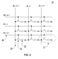
- FIG. 2 is a diagram illustrating a PCM RAM array
- FIG. 3 is a diagram illustrating a PCM-CAM cell, according to an embodiment of the invention.
- FIG. 4 is a diagram illustrating a PCM-CAM array and peripheral blocks, according to an embodiment of the invention.
- FIG. 5 is a diagram illustrating a read, write and search line driver, according to an embodiment of the invention.
- FIG. 6 is a match-line control block, according to an embodiment of the invention.
- Nonvolatile memory using phase change materials such as Chalcogenides
- PCM phase change materials
- Chalcogenides refers to the Group VI elements of the periodic table.
- Chalcogenide refers to materials containing at least one of these elements such as the alloy of germanium, antimony, and tellurium, etc.
- the Chalcogenide phase change material e.g., Ge 2 Sb 2 Te 5 , can be programmed and reprogrammed into a large range of resistance states.
- PCM-based memory data programming is achieved through thermally induced structural phase changes when electrical pulses are applied to the Chalcogenide resistors.
- a high current, short pulse will lead to the amorphous phase (or so called “reset” state) with high resistance.
- a lower and longer current pulse will lead to the crystalline phase with low resistance (or called low resistance “set” state).
- Read operation is performed with an even lower current that does not cause any phase change.
- the ratio of the resistance between two states can be greater than 1,000 times, which provides a high sensing margin.
- U.S. Pat. No. 6,885,602 discloses that in a write operation, when a current is applied to the PCM to generate a temperature greater than or equal to its melting temperature and then the PCM is rapidly cooled down, the PCM becomes amorphous and data ‘1’ may be recorded in the PCM. In this case, the PCM is said to have entered a “reset” state. If the PCM is heated at a temperature greater than or equal to a crystallization temperature, maintained for a given time, and cooled down, the PCM becomes crystalline and data ‘0’ may be recorded in the PCM. In this case, the PCM is said to have entered a “set” state.
- a resistance of the PCM changes.
- a voltage changes, thus allowing the expression of binary values ‘1’ and ‘0’.
- a bit-line and a word-line may be selected to choose a particular memory cell.
- FIG. 2 shows a typical implementation of a phase change material (PCM) random access memory (RAM) array 20 , which is an array of PCM RAM cells 21 .
- the array comprises a plurality of wordlines and a plurality of bitlines, and a two dimensional matrix of cells.
- a PCM-RAM cell 21 comprises: (1) a phase change material 22 , represented by a small circle, with one end connected to a voltage source VA; (2) a n-type field effect transistor (nFET) 23 that has its gate connected to the word-line (WL) 24 and its source and drain connected to the bitline (BL) 25 and the phase change material 22 , respectively. Only one wordline in the array is activated in the write and read operation.
- PCM phase change material
- a content addressable memory (CAM) using phase change material is provided.
- the phase-change-material content addressable memory (PCM-CAM) is a system comprising an array of PCM-CAM cells, and peripheral circuits for the content addressable memory (CAM) operation, and for the random access memory (RAM) operation.
- FIG. 3 shows an illustrative embodiment of a phase-change-material-content-addressable-memory (PCM-CAM) cell 30 .
- PCM-CAM cell 30 comprises: (1) a first phase change material element 32 represented by a small circle, with one end connected to the Match-Line (ML) 31 ; (2) a first transistor (e.g., n-channel field effect transistor) 33 that has its gate connected to the word-line (WL) 34 and its source and drain connected to the true Bit-read-write-Search-Line (BSL) 35 and the first phase change material element 32 , respectively; (3) a second phase change material element 32 b represented by a small circle, with one end connected to the Match-Line (ML) 31 ; (4) a second transistor (e.g., n-channel field effect transistor) 33 b that has its gate connected to the word-line (WL) 34 and its source and drain connected to the complementary Bit-read-write-Search-Line (bBSL) 35 b and the second phase change material element 32
- Table 1 describes write and read operations in the RAM mode, while Table 2 describes precharge and search operations in the CAM mode.
- bBSL is driven low while BSL is set to be floating or weakly high (so that it does not charge up the ML during a mismatch). If the Data is “0”, match-line (ML) will stay high since it has a high resistance path to bBSL. If the Data is “1”, ML will be discharged to low since it has a low resistance path to bBSL. Similarly, in the search for “1” operation, BSL is driven low while bBSL is set to be floating or weakly high.
- the current through the phase change material should be limited to be less than the threshold value, in order to avoid overwriting the stored data during CAM operation.
- each word-line and corresponding match-line are connected to a number of cells. If any one cell is a mismatch, the match-line line will be driven low. If all cells are matching, then the match-line will stay high.
- a PCM-CAM array 40 comprises a plurality of Word-Lines (WL) and Match-Lines (ML), a plurality of true Bit-read-write-Search-Lines (BL-SL) and complementary Bit-read-write-Search-Lines (bBSL), and a two dimensional matrix of PCM-CAM cells 30 (as shown in FIG. 3 ).
- Each pair of true and complementary Bit-read-write-Search-Lines (BSL and bBSL) is connected to a Read, Write & Search Line (SL) Driver block 50 .
- the Read, Write & SL Driver block 50 performs the read and write operations in RAM mode, and also drives the data to be compared with the CAM cells in the CAM mode.
- Each Match-Line (ML) is connected to a Match-line (ML) Control block 60 .
- the Match-line (ML) Control block 60 provides the Match-Line (ML) with a positive voltage source (as the voltage source VA in the conventional PCM).
- a Word-Line driver block 70 functions as a conventional WL decoder and driver, and activates only one wordline in the RAM mode.
- Word-Line driver block 70 drives all Word-Lines to a high voltage level (e.g., 1.5V ⁇ 3.5V).
- the Read, Write, and Search-Line Driver 50 is shown in FIG. 5 .
- the signals SET, RESET and READ are used to switch the corresponding transistors to perform write 0, write 1 and read operation. Appropriate transistor sizing will set the pulse current in the range required.
- the Match-Line control block 60 is shown in FIG. 6 .
- this block precharges the Match-Line to the voltage level VA (e.g., 1.0V ⁇ 2.0V).
- VA voltage level
- CAM CAM mode
- block 60 precharges the Match-Line to a high level (e.g., 1.0V ⁇ 2.0V) in the precharge phase and performs the sense operation in the evaluation phase.
- both BSL and bBSL By de-activating one or a group of word-lines (e.g., by not driving them), the corresponding word-lines will be masked and not participate in the CAM search operation.
- BSL and bBSL By setting both BSL and bBSL to be floating or weak high (e.g., 0.5V ⁇ 2.0V), instead of having one of them low), the corresponding search line is blocked.
Landscapes
- Chemical & Material Sciences (AREA)
- Crystallography & Structural Chemistry (AREA)
- Semiconductor Memories (AREA)
Priority Applications (6)
| Application Number | Priority Date | Filing Date | Title |
|---|---|---|---|
| US11/172,473 US7319608B2 (en) | 2005-06-30 | 2005-06-30 | Non-volatile content addressable memory using phase-change-material memory elements |
| PCT/US2006/008550 WO2007005067A1 (en) | 2005-06-30 | 2006-03-09 | Non-volatile content addressable memory using phase-change-material memory elements |
| JP2008519262A JP4378425B2 (ja) | 2005-06-30 | 2006-03-09 | 相変化材料メモリ素子を利用する不揮発性連想メモリ |
| CN2006800166509A CN101176161B (zh) | 2005-06-30 | 2006-03-09 | 使用相变材料存储器元件的非易失性内容可寻址存储器 |
| EP06737703A EP1908076A4 (en) | 2005-06-30 | 2006-03-09 | NON-VOLATILE CONTENT ADDRESSABLE MEMORY USING PHASE CHANGE MATERIAL MEMORY ELEMENTS |
| TW095122923A TWI396198B (zh) | 2005-06-30 | 2006-06-26 | 使用相變材料記憶元件的非揮發性內容可定址記憶體 |
Applications Claiming Priority (1)
| Application Number | Priority Date | Filing Date | Title |
|---|---|---|---|
| US11/172,473 US7319608B2 (en) | 2005-06-30 | 2005-06-30 | Non-volatile content addressable memory using phase-change-material memory elements |
Publications (2)
| Publication Number | Publication Date |
|---|---|
| US20070002608A1 US20070002608A1 (en) | 2007-01-04 |
| US7319608B2 true US7319608B2 (en) | 2008-01-15 |
Family
ID=37589273
Family Applications (1)
| Application Number | Title | Priority Date | Filing Date |
|---|---|---|---|
| US11/172,473 Active US7319608B2 (en) | 2005-06-30 | 2005-06-30 | Non-volatile content addressable memory using phase-change-material memory elements |
Country Status (6)
| Country | Link |
|---|---|
| US (1) | US7319608B2 (zh) |
| EP (1) | EP1908076A4 (zh) |
| JP (1) | JP4378425B2 (zh) |
| CN (1) | CN101176161B (zh) |
| TW (1) | TWI396198B (zh) |
| WO (1) | WO2007005067A1 (zh) |
Cited By (15)
| Publication number | Priority date | Publication date | Assignee | Title |
|---|---|---|---|---|
| US20100163817A1 (en) * | 2008-12-30 | 2010-07-01 | Stmicroelectronics, S.R.L. | Self-heating phase change memory cell architecture |
| US20100226161A1 (en) * | 2009-03-06 | 2010-09-09 | Ji Brian L | Ternary content addressable memory using phase change devices |
| US20100265748A1 (en) * | 2009-04-21 | 2010-10-21 | Lam Chung H | High density ternary content addressable memory |
| US20110051482A1 (en) * | 2009-08-28 | 2011-03-03 | International Business Machines Corporation | Content addressable memory array programmed to perform logic operations |
| US20110051485A1 (en) * | 2009-08-28 | 2011-03-03 | International Business Machines Corporation | Content addressable memory array writing |
| US20110051483A1 (en) * | 2009-08-28 | 2011-03-03 | International Business Machines Corporation | Content addressable memory array |
| US20110051486A1 (en) * | 2009-08-28 | 2011-03-03 | International Business Machines Corporation | Content addressable memory reference clock |
| US8446748B2 (en) | 2011-08-04 | 2013-05-21 | International Business Machines Corporation | Content addressable memories with wireline compensation |
| US8497705B2 (en) | 2010-11-09 | 2013-07-30 | Macronix International Co., Ltd. | Phase change device for interconnection of programmable logic device |
| US8908407B1 (en) * | 2011-07-30 | 2014-12-09 | Rambus Inc. | Content addressable memory (“CAM”) |
| US9269042B2 (en) | 2010-09-30 | 2016-02-23 | International Business Machines Corporation | Producing spike-timing dependent plasticity in a neuromorphic network utilizing phase change synaptic devices |
| US9754668B1 (en) * | 2016-03-03 | 2017-09-05 | Flashsilicon Incorporation | Digital perceptron |
| US10229738B2 (en) | 2017-04-25 | 2019-03-12 | International Business Machines Corporation | SRAM bitline equalization using phase change material |
| US11031079B1 (en) | 2019-11-27 | 2021-06-08 | Flashsilicon Incorporation | Dynamic digital perceptron |
| US11600320B2 (en) | 2019-12-17 | 2023-03-07 | Flashsilicon Incorporation | Perpectual digital perceptron |
Families Citing this family (17)
| Publication number | Priority date | Publication date | Assignee | Title |
|---|---|---|---|---|
| US7675765B2 (en) * | 2005-11-03 | 2010-03-09 | Agate Logic, Inc. | Phase-change memory (PCM) based universal content-addressable memory (CAM) configured as binary/ternary CAM |
| US7447053B2 (en) * | 2006-03-07 | 2008-11-04 | Infineon Technologies Ag | Memory device and method for operating such a memory device |
| KR100900199B1 (ko) * | 2006-09-19 | 2009-06-02 | 삼성전자주식회사 | 상변화 메모리를 이용하는 캠(ContentAddressable Memory ; CAM) 셀 및 캠 |
| US7782646B2 (en) * | 2008-06-30 | 2010-08-24 | International Business Machines Corporation | High density content addressable memory using phase change devices |
| US7881089B2 (en) | 2009-02-24 | 2011-02-01 | International Business Machines Corporation | Coding techniques for improving the sense margin in content addressable memories |
| US8521952B2 (en) * | 2009-03-31 | 2013-08-27 | Micron Technology, Inc. | Hierarchical memory architecture with a phase-change memory (PCM) content addressable memory (CAM) |
| US20100250798A1 (en) * | 2009-03-31 | 2010-09-30 | Sean Eilert | Hierarchical memory architecture with an interface to differing memory formats |
| JP5907524B2 (ja) * | 2011-02-25 | 2016-04-26 | 国立大学法人東北大学 | 不揮発機能メモリ装置 |
| US8729545B2 (en) | 2011-04-28 | 2014-05-20 | Semiconductor Energy Laboratory Co., Ltd. | Semiconductor memory device |
| CN104463187B (zh) * | 2014-10-22 | 2018-11-16 | 宁波力芯科信息科技有限公司 | 综合隶属函数发生器阵列及模糊识别器 |
| US10741585B2 (en) * | 2018-06-29 | 2020-08-11 | Sandisk Technologies Llc | Content addressable memory using threshold-adjustable vertical transistors and methods of forming the same |
| CN111128278B (zh) | 2018-10-30 | 2021-08-27 | 华为技术有限公司 | 内容寻址存储器、数据处理方法及网络设备 |
| US11289162B2 (en) * | 2020-04-30 | 2022-03-29 | Hewlett Packard Enterprise Development Lp | Analog content addressable memory utilizing three terminal memory devices |
| TWI766706B (zh) * | 2020-08-26 | 2022-06-01 | 旺宏電子股份有限公司 | 三態內容可定址記憶體以及用於其之決策產生方法 |
| CN113012731B (zh) * | 2021-02-26 | 2023-05-09 | 西安微电子技术研究所 | 一种适用于大位宽cam的数据锁存电路结构 |
| CN114743578B (zh) * | 2022-04-06 | 2024-05-17 | 北京大学 | 基于铁电隧穿场效应晶体管FeTFET实现三态内容可寻址存储器TCAM的方法 |
| CN114758695B (zh) * | 2022-04-06 | 2024-05-17 | 北京大学 | 基于铁电隧穿场效应晶体管FeTFET实现多值内容可寻址存储器MCAM的方法 |
Citations (10)
| Publication number | Priority date | Publication date | Assignee | Title |
|---|---|---|---|---|
| US5111427A (en) | 1988-06-01 | 1992-05-05 | Mitsubishi Denki Kabushiki Kaisha | Nonvolatile content-addressable memory and operating method therefor |
| US5296716A (en) | 1991-01-18 | 1994-03-22 | Energy Conversion Devices, Inc. | Electrically erasable, directly overwritable, multibit single cell memory elements and arrays fabricated therefrom |
| US6191973B1 (en) | 1999-09-27 | 2001-02-20 | Motorola Inc. | Mram cam |
| US6269016B1 (en) | 2000-06-19 | 2001-07-31 | Motorola Inc. | MRAM cam |
| US6317349B1 (en) * | 1999-04-16 | 2001-11-13 | Sandisk Corporation | Non-volatile content addressable memory |
| US6738278B2 (en) * | 2002-08-10 | 2004-05-18 | Samsung Electronics Co., Ltd. | Cache memory device including word line driver circuit and method |
| US6885602B2 (en) | 2003-08-22 | 2005-04-26 | Samsung Electronics Co., Ltd. | Programming method of controlling the amount of write current applied to phase change memory device and write driver circuit therefor |
| US20050169095A1 (en) * | 2003-10-22 | 2005-08-04 | Stmicroelectronics S.R.L. | Bit line discharge control method and circuit for a semiconductor memory |
| US20060018183A1 (en) * | 2003-10-22 | 2006-01-26 | Stmicroelectronics S.R.L. | Content addressable memory cell |
| US20060067097A1 (en) * | 2004-09-24 | 2006-03-30 | Chuen-Der Lien | Binary and ternary non-volatile CAM |
Family Cites Families (10)
| Publication number | Priority date | Publication date | Assignee | Title |
|---|---|---|---|---|
| US5305262A (en) * | 1991-09-11 | 1994-04-19 | Kawasaki Steel Corporation | Semiconductor integrated circuit |
| US6314014B1 (en) * | 1999-12-16 | 2001-11-06 | Ovonyx, Inc. | Programmable resistance memory arrays with reference cells |
| US6639818B1 (en) * | 2000-03-16 | 2003-10-28 | Silicon Storage Technology, Inc. | Differential non-volatile content addressable memory cell and array |
| US6759267B2 (en) * | 2002-07-19 | 2004-07-06 | Macronix International Co., Ltd. | Method for forming a phase change memory |
| EP1420412B1 (en) * | 2002-11-18 | 2008-07-09 | STMicroelectronics S.r.l. | Circuit and method for temperature tracing of devices including an element of chalcogenic material, in particular phase change memory devices |
| US6912146B2 (en) * | 2002-12-13 | 2005-06-28 | Ovonyx, Inc. | Using an MOS select gate for a phase change memory |
| KR100479810B1 (ko) * | 2002-12-30 | 2005-03-31 | 주식회사 하이닉스반도체 | 불휘발성 메모리 장치 |
| JP2004288282A (ja) * | 2003-03-20 | 2004-10-14 | Fujitsu Ltd | 半導体装置 |
| CN1717748A (zh) * | 2003-06-25 | 2006-01-04 | 松下电器产业株式会社 | 驱动非易失性存储器的方法 |
| KR100569549B1 (ko) * | 2003-12-13 | 2006-04-10 | 주식회사 하이닉스반도체 | 상 변화 저항 셀 및 이를 이용한 불휘발성 메모리 장치 |
-
2005
- 2005-06-30 US US11/172,473 patent/US7319608B2/en active Active
-
2006
- 2006-03-09 WO PCT/US2006/008550 patent/WO2007005067A1/en active Application Filing
- 2006-03-09 EP EP06737703A patent/EP1908076A4/en not_active Withdrawn
- 2006-03-09 JP JP2008519262A patent/JP4378425B2/ja not_active Expired - Fee Related
- 2006-03-09 CN CN2006800166509A patent/CN101176161B/zh active Active
- 2006-06-26 TW TW095122923A patent/TWI396198B/zh not_active IP Right Cessation
Patent Citations (10)
| Publication number | Priority date | Publication date | Assignee | Title |
|---|---|---|---|---|
| US5111427A (en) | 1988-06-01 | 1992-05-05 | Mitsubishi Denki Kabushiki Kaisha | Nonvolatile content-addressable memory and operating method therefor |
| US5296716A (en) | 1991-01-18 | 1994-03-22 | Energy Conversion Devices, Inc. | Electrically erasable, directly overwritable, multibit single cell memory elements and arrays fabricated therefrom |
| US6317349B1 (en) * | 1999-04-16 | 2001-11-13 | Sandisk Corporation | Non-volatile content addressable memory |
| US6191973B1 (en) | 1999-09-27 | 2001-02-20 | Motorola Inc. | Mram cam |
| US6269016B1 (en) | 2000-06-19 | 2001-07-31 | Motorola Inc. | MRAM cam |
| US6738278B2 (en) * | 2002-08-10 | 2004-05-18 | Samsung Electronics Co., Ltd. | Cache memory device including word line driver circuit and method |
| US6885602B2 (en) | 2003-08-22 | 2005-04-26 | Samsung Electronics Co., Ltd. | Programming method of controlling the amount of write current applied to phase change memory device and write driver circuit therefor |
| US20050169095A1 (en) * | 2003-10-22 | 2005-08-04 | Stmicroelectronics S.R.L. | Bit line discharge control method and circuit for a semiconductor memory |
| US20060018183A1 (en) * | 2003-10-22 | 2006-01-26 | Stmicroelectronics S.R.L. | Content addressable memory cell |
| US20060067097A1 (en) * | 2004-09-24 | 2006-03-30 | Chuen-Der Lien | Binary and ternary non-volatile CAM |
Non-Patent Citations (1)
| Title |
|---|
| G. Wicker et al., "Nonvolatile, High Density, High Performance Phase Change Memory," Ovonyx, Inc., Mission Research Corporation, pp. 1-8, Sep. 1999. |
Cited By (25)
| Publication number | Priority date | Publication date | Assignee | Title |
|---|---|---|---|---|
| US20100163817A1 (en) * | 2008-12-30 | 2010-07-01 | Stmicroelectronics, S.R.L. | Self-heating phase change memory cell architecture |
| US8377741B2 (en) * | 2008-12-30 | 2013-02-19 | Stmicroelectronics S.R.L. | Self-heating phase change memory cell architecture |
| US20100226161A1 (en) * | 2009-03-06 | 2010-09-09 | Ji Brian L | Ternary content addressable memory using phase change devices |
| US8120937B2 (en) * | 2009-03-06 | 2012-02-21 | International Business Machines Corporation | Ternary content addressable memory using phase change devices |
| US20100265748A1 (en) * | 2009-04-21 | 2010-10-21 | Lam Chung H | High density ternary content addressable memory |
| US7872889B2 (en) | 2009-04-21 | 2011-01-18 | International Business Machines Corporation | High density ternary content addressable memory |
| US20110051483A1 (en) * | 2009-08-28 | 2011-03-03 | International Business Machines Corporation | Content addressable memory array |
| US20110051486A1 (en) * | 2009-08-28 | 2011-03-03 | International Business Machines Corporation | Content addressable memory reference clock |
| US7948782B2 (en) | 2009-08-28 | 2011-05-24 | International Business Machines Corporation | Content addressable memory reference clock |
| US8054662B2 (en) | 2009-08-28 | 2011-11-08 | International Business Machines Corporation | Content addressable memory array |
| US8059438B2 (en) | 2009-08-28 | 2011-11-15 | International Business Machines Corporation | Content addressable memory array programmed to perform logic operations |
| US20110051485A1 (en) * | 2009-08-28 | 2011-03-03 | International Business Machines Corporation | Content addressable memory array writing |
| US20110051482A1 (en) * | 2009-08-28 | 2011-03-03 | International Business Machines Corporation | Content addressable memory array programmed to perform logic operations |
| US9953261B2 (en) | 2010-09-30 | 2018-04-24 | International Business Machines Corporation | Producing spike-timing dependent plasticity in a neuromorphic network utilizing phase change synaptic devices |
| US9269042B2 (en) | 2010-09-30 | 2016-02-23 | International Business Machines Corporation | Producing spike-timing dependent plasticity in a neuromorphic network utilizing phase change synaptic devices |
| US9946969B2 (en) | 2010-09-30 | 2018-04-17 | International Business Machines Corporation | Producing spike-timing dependent plasticity in a neuromorphic network utilizing phase change synaptic devices |
| US11232345B2 (en) | 2010-09-30 | 2022-01-25 | International Business Machines Corporation | Producing spike-timing dependent plasticity in a neuromorphic network utilizing phase change synaptic devices |
| US11270192B2 (en) | 2010-09-30 | 2022-03-08 | International Business Machines Corporation | Producing spike-timing dependent plasticity in a neuromorphic network utilizing phase change synaptic devices |
| US8497705B2 (en) | 2010-11-09 | 2013-07-30 | Macronix International Co., Ltd. | Phase change device for interconnection of programmable logic device |
| US8908407B1 (en) * | 2011-07-30 | 2014-12-09 | Rambus Inc. | Content addressable memory (“CAM”) |
| US8446748B2 (en) | 2011-08-04 | 2013-05-21 | International Business Machines Corporation | Content addressable memories with wireline compensation |
| US9754668B1 (en) * | 2016-03-03 | 2017-09-05 | Flashsilicon Incorporation | Digital perceptron |
| US10229738B2 (en) | 2017-04-25 | 2019-03-12 | International Business Machines Corporation | SRAM bitline equalization using phase change material |
| US11031079B1 (en) | 2019-11-27 | 2021-06-08 | Flashsilicon Incorporation | Dynamic digital perceptron |
| US11600320B2 (en) | 2019-12-17 | 2023-03-07 | Flashsilicon Incorporation | Perpectual digital perceptron |
Also Published As
| Publication number | Publication date |
|---|---|
| TWI396198B (zh) | 2013-05-11 |
| JP2008545221A (ja) | 2008-12-11 |
| EP1908076A1 (en) | 2008-04-09 |
| EP1908076A4 (en) | 2009-06-17 |
| CN101176161A (zh) | 2008-05-07 |
| CN101176161B (zh) | 2012-08-08 |
| JP4378425B2 (ja) | 2009-12-09 |
| TW200741707A (en) | 2007-11-01 |
| WO2007005067A1 (en) | 2007-01-11 |
| US20070002608A1 (en) | 2007-01-04 |
Similar Documents
| Publication | Publication Date | Title |
|---|---|---|
| US7319608B2 (en) | Non-volatile content addressable memory using phase-change-material memory elements | |
| US8199603B2 (en) | Nonvolatile memory devices having variable-resistance memory cells and methods of programming the same | |
| US7675765B2 (en) | Phase-change memory (PCM) based universal content-addressable memory (CAM) configured as binary/ternary CAM | |
| US7215592B2 (en) | Memory device with reduced word line resistance | |
| US7457152B2 (en) | Non-volatile memory devices and systems including phase-change one-time-programmable (OTP) memory cells and related methods | |
| US7453722B2 (en) | Phase change memory device and memory cell array thereof | |
| US7471553B2 (en) | Phase change memory device and program method thereof | |
| US7570507B2 (en) | Quasi-differential read operation | |
| US20070041242A1 (en) | Nonvolatile memory cell, storage device and nonvolatile logic circuit | |
| US7778071B2 (en) | Phase change memory device having decentralized driving units | |
| US7227765B2 (en) | Content addressable memory cell | |
| US20150243356A1 (en) | High throughput programming system and method for a phase change non-volatile memory device | |
| US20240153553A1 (en) | Non-volatile phase-change memory device including a distributed row decoder with n-channel mosfet transistors and related row decoding method | |
| EP1684306B1 (en) | Phase change memory device and data writing method | |
| EP1733398B1 (en) | Circuit for accessing a chalcogenide memory array | |
| JP3581170B2 (ja) | 半導体記憶装置 | |
| US11475960B2 (en) | Non-volatile memory device with a program driver circuit including a voltage limiter | |
| US20240177770A1 (en) | Non-volatile memory structure with single cell or twin cell sensing |
Legal Events
| Date | Code | Title | Description |
|---|---|---|---|
| AS | Assignment |
Owner name: INTERNATIONAL BUSINESS MACHINES CORPORATION, NEW Y Free format text: ASSIGNMENT OF ASSIGNORS INTEREST;ASSIGNORS:HSU, LOUIS L.C.;JI, BRIAN L.;LAM, CHUNG HON;AND OTHERS;REEL/FRAME:016624/0271;SIGNING DATES FROM 20050801 TO 20050802 |
|
| FEPP | Fee payment procedure |
Free format text: PAYOR NUMBER ASSIGNED (ORIGINAL EVENT CODE: ASPN); ENTITY STATUS OF PATENT OWNER: LARGE ENTITY |
|
| STCF | Information on status: patent grant |
Free format text: PATENTED CASE |
|
| FPAY | Fee payment |
Year of fee payment: 4 |
|
| FPAY | Fee payment |
Year of fee payment: 8 |
|
| AS | Assignment |
Owner name: GLOBALFOUNDRIES U.S. 2 LLC, NEW YORK Free format text: ASSIGNMENT OF ASSIGNORS INTEREST;ASSIGNOR:INTERNATIONAL BUSINESS MACHINES CORPORATION;REEL/FRAME:036550/0001 Effective date: 20150629 |
|
| AS | Assignment |
Owner name: GLOBALFOUNDRIES INC., CAYMAN ISLANDS Free format text: ASSIGNMENT OF ASSIGNORS INTEREST;ASSIGNORS:GLOBALFOUNDRIES U.S. 2 LLC;GLOBALFOUNDRIES U.S. INC.;REEL/FRAME:036779/0001 Effective date: 20150910 |
|
| AS | Assignment |
Owner name: WILMINGTON TRUST, NATIONAL ASSOCIATION, DELAWARE Free format text: SECURITY AGREEMENT;ASSIGNOR:GLOBALFOUNDRIES INC.;REEL/FRAME:049490/0001 Effective date: 20181127 |
|
| MAFP | Maintenance fee payment |
Free format text: PAYMENT OF MAINTENANCE FEE, 12TH YEAR, LARGE ENTITY (ORIGINAL EVENT CODE: M1553); ENTITY STATUS OF PATENT OWNER: LARGE ENTITY Year of fee payment: 12 |
|
| AS | Assignment |
Owner name: GLOBALFOUNDRIES U.S. INC., CALIFORNIA Free format text: ASSIGNMENT OF ASSIGNORS INTEREST;ASSIGNOR:GLOBALFOUNDRIES INC.;REEL/FRAME:054633/0001 Effective date: 20201022 |
|
| AS | Assignment |
Owner name: GLOBALFOUNDRIES INC., CAYMAN ISLANDS Free format text: RELEASE BY SECURED PARTY;ASSIGNOR:WILMINGTON TRUST, NATIONAL ASSOCIATION;REEL/FRAME:054636/0001 Effective date: 20201117 |
|
| AS | Assignment |
Owner name: GLOBALFOUNDRIES U.S. INC., NEW YORK Free format text: RELEASE BY SECURED PARTY;ASSIGNOR:WILMINGTON TRUST, NATIONAL ASSOCIATION;REEL/FRAME:056987/0001 Effective date: 20201117 |