US7288997B2 - Phase lock loop and the control method thereof - Google Patents
Phase lock loop and the control method thereof Download PDFInfo
- Publication number
- US7288997B2 US7288997B2 US11/068,622 US6862205A US7288997B2 US 7288997 B2 US7288997 B2 US 7288997B2 US 6862205 A US6862205 A US 6862205A US 7288997 B2 US7288997 B2 US 7288997B2
- Authority
- US
- United States
- Prior art keywords
- clock
- frequency
- voltage
- select
- lock loop
- Prior art date
- Legal status (The legal status is an assumption and is not a legal conclusion. Google has not performed a legal analysis and makes no representation as to the accuracy of the status listed.)
- Active
Links
- 238000000034 method Methods 0.000 title claims abstract description 12
- 230000000052 comparative effect Effects 0.000 claims description 11
- 230000008859 change Effects 0.000 claims description 4
- 230000007423 decrease Effects 0.000 claims 1
- 238000010586 diagram Methods 0.000 description 17
- 230000000630 rising effect Effects 0.000 description 7
- 230000001960 triggered effect Effects 0.000 description 5
- 230000009471 action Effects 0.000 description 4
- 230000004044 response Effects 0.000 description 3
- 238000012986 modification Methods 0.000 description 2
- 230000004048 modification Effects 0.000 description 2
- 230000008901 benefit Effects 0.000 description 1
- 230000003247 decreasing effect Effects 0.000 description 1
- 238000005516 engineering process Methods 0.000 description 1
- 229920000729 poly(L-lysine) polymer Polymers 0.000 description 1
- 230000007704 transition Effects 0.000 description 1
Images


Classifications
-
- H—ELECTRICITY
- H03—ELECTRONIC CIRCUITRY
- H03L—AUTOMATIC CONTROL, STARTING, SYNCHRONISATION OR STABILISATION OF GENERATORS OF ELECTRONIC OSCILLATIONS OR PULSES
- H03L7/00—Automatic control of frequency or phase; Synchronisation
- H03L7/06—Automatic control of frequency or phase; Synchronisation using a reference signal applied to a frequency- or phase-locked loop
- H03L7/16—Indirect frequency synthesis, i.e. generating a desired one of a number of predetermined frequencies using a frequency- or phase-locked loop
- H03L7/18—Indirect frequency synthesis, i.e. generating a desired one of a number of predetermined frequencies using a frequency- or phase-locked loop using a frequency divider or counter in the loop
- H03L7/183—Indirect frequency synthesis, i.e. generating a desired one of a number of predetermined frequencies using a frequency- or phase-locked loop using a frequency divider or counter in the loop a time difference being used for locking the loop, the counter counting between fixed numbers or the frequency divider dividing by a fixed number
-
- H—ELECTRICITY
- H03—ELECTRONIC CIRCUITRY
- H03L—AUTOMATIC CONTROL, STARTING, SYNCHRONISATION OR STABILISATION OF GENERATORS OF ELECTRONIC OSCILLATIONS OR PULSES
- H03L7/00—Automatic control of frequency or phase; Synchronisation
- H03L7/06—Automatic control of frequency or phase; Synchronisation using a reference signal applied to a frequency- or phase-locked loop
- H03L7/08—Details of the phase-locked loop
- H03L7/085—Details of the phase-locked loop concerning mainly the frequency- or phase-detection arrangement including the filtering or amplification of its output signal
- H03L7/087—Details of the phase-locked loop concerning mainly the frequency- or phase-detection arrangement including the filtering or amplification of its output signal using at least two phase detectors or a frequency and phase detector in the loop
-
- H—ELECTRICITY
- H03—ELECTRONIC CIRCUITRY
- H03L—AUTOMATIC CONTROL, STARTING, SYNCHRONISATION OR STABILISATION OF GENERATORS OF ELECTRONIC OSCILLATIONS OR PULSES
- H03L7/00—Automatic control of frequency or phase; Synchronisation
- H03L7/06—Automatic control of frequency or phase; Synchronisation using a reference signal applied to a frequency- or phase-locked loop
- H03L7/08—Details of the phase-locked loop
- H03L7/085—Details of the phase-locked loop concerning mainly the frequency- or phase-detection arrangement including the filtering or amplification of its output signal
- H03L7/089—Details of the phase-locked loop concerning mainly the frequency- or phase-detection arrangement including the filtering or amplification of its output signal the phase or frequency detector generating up-down pulses
- H03L7/0891—Details of the phase-locked loop concerning mainly the frequency- or phase-detection arrangement including the filtering or amplification of its output signal the phase or frequency detector generating up-down pulses the up-down pulses controlling source and sink current generators, e.g. a charge pump
-
- H—ELECTRICITY
- H03—ELECTRONIC CIRCUITRY
- H03L—AUTOMATIC CONTROL, STARTING, SYNCHRONISATION OR STABILISATION OF GENERATORS OF ELECTRONIC OSCILLATIONS OR PULSES
- H03L7/00—Automatic control of frequency or phase; Synchronisation
- H03L7/06—Automatic control of frequency or phase; Synchronisation using a reference signal applied to a frequency- or phase-locked loop
- H03L7/08—Details of the phase-locked loop
- H03L7/099—Details of the phase-locked loop concerning mainly the controlled oscillator of the loop
- H03L7/0995—Details of the phase-locked loop concerning mainly the controlled oscillator of the loop the oscillator comprising a ring oscillator
-
- H—ELECTRICITY
- H03—ELECTRONIC CIRCUITRY
- H03L—AUTOMATIC CONTROL, STARTING, SYNCHRONISATION OR STABILISATION OF GENERATORS OF ELECTRONIC OSCILLATIONS OR PULSES
- H03L7/00—Automatic control of frequency or phase; Synchronisation
- H03L7/06—Automatic control of frequency or phase; Synchronisation using a reference signal applied to a frequency- or phase-locked loop
- H03L7/08—Details of the phase-locked loop
- H03L7/10—Details of the phase-locked loop for assuring initial synchronisation or for broadening the capture range
- H03L7/113—Details of the phase-locked loop for assuring initial synchronisation or for broadening the capture range using frequency discriminator
-
- H—ELECTRICITY
- H03—ELECTRONIC CIRCUITRY
- H03L—AUTOMATIC CONTROL, STARTING, SYNCHRONISATION OR STABILISATION OF GENERATORS OF ELECTRONIC OSCILLATIONS OR PULSES
- H03L2207/00—Indexing scheme relating to automatic control of frequency or phase and to synchronisation
- H03L2207/06—Phase locked loops with a controlled oscillator having at least two frequency control terminals
Definitions
- the invention relates to a phase lock loop, and more specifically to a phase lock loop capable of adjusting states automatically and control method thereof.
- FIG. 1A is a block diagram of a conventional phase lock loop (PLL), having a phase/frequency detector (PFD) 90 , a charge pump 92 , a voltage-controlled oscillator (VCO) 94 , and a frequency divider 96 .
- the PFD 90 detects the transitional edges of the feedback clock Clk fb and the reference clock Clk ref to generate comparative signals UP and DN which, in turn, charge and discharge the charge pump 92 to generate a control voltage V c .
- the VCO 94 generates an output clock Clk vco of variable frequency in response to the control voltage V c .
- the frequency divider 96 divides the frequency of the clock Clk vco to generate the feedback clock Clk fb .
- VCO is generally designed to operate in a single state, having a single voltage frequency transfer curve.
- VCOs There are two types of VCOs in terms of the voltage-frequency transfer curve slope, high gain and low gain VCOs.
- FIG. 1B shows two voltage-frequency transfer curves A and B, corresponding to high gain and low gain VCOs respectively.
- high gain VCO provides the advantage of broader tuning frequency range.
- the performance of the output clock stability in high gain VCO is inferior since frequency of the output clock is susceptible to the change in control voltage V c .
- low gain VCO provides a more stable frequency of the output clock but a narrower tuning frequency range.
- selecting a suitable voltage-frequency transfer curve for a VCO has been important for circuit designers.
- the present invention is generally directed to a phase lock loop capable of adjusting operating states automatically.
- the phase lock loop generates a feedback clock for tracing a reference clock, the phase lock loop comprising a phase/frequency detector, a charge pump, a voltage-controlled oscillator and a state select circuit.
- the phase/frequency detector (PFD) compares phase difference between the feedback clock and the reference clock to generate a comparative signal.
- the charge pump generates a control voltage to the voltage-controlled oscillator (VCO).
- VCO voltage-controlled oscillator
- the VCO then operates in one of the select states to generate an oscillating clock according to the control voltage and a select voltage wherein the ratio of the frequency of the oscillating clock to the frequency of the feedback clock is an integer.
- the state select circuit adjusts the select voltage in accordance with the reference clock to select one of the select sates.
- a method for controlling a phase lock loop comprising generating first and second clocks corresponding to the highest and lowest frequency oscillating clocks respectively, generated by the phase lock loop when operating in one of the select states, comparing the frequencies of the first and second clocks to the frequency of the reference clock respectively, thereby holding the select state of the phase lock loop when the first, second, and reference clocks are in a first predetermined condition; or changing the select state of the phase lock loop when in a second predetermined condition.
- FIG. 1A is a block diagram of a related art phase lock loop.
- FIG. 1B is a schematic diagram of two voltage-frequency transfer curves A and B in a VCO.
- FIG. 2 is a schematic diagram of the voltage-frequency transfer curves in a VCO according to an embodiment of the invention.
- FIG. 3 is a flow diagram illustrating an embodiment of the invention.
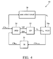
- FIG. 4 is a block diagram of a phase lock loop according to an embodiment of the invention.
- FIG. 5 is a block diagram of the state select circuit in FIG. 4 .
- FIG. 6 is a schematic diagram of the frequency comparator in FIG. 5 .
- FIG. 7 is a schematic diagram of the weight refreshing circuit in FIG. 5 .
- FIG. 8 is a schematic diagram of the select voltage generating circuit in FIG. 5 .
- FIG. 9 is a schematic diagram of a VCO.
- FIG. 10 is a schematic diagram of a delay device in FIG. 9 .
- FIG. 2 shows the voltage-frequency transfer curves of a VCO according to an embodiment of the invention.
- the VCO is capable of operating in a plurality of select states, S, and each select state S corresponds to a voltage-frequency transfer curve.
- V min and V max in x-axis denote the maximum and minimum values of the input control voltage V C in the VCO, respectively and the denotation, f L,S in y-axis, denotes the frequency of the feedback clock generated by the frequency divider with the VCO when the VCO operates in a select state S and the control voltage V C is V min .
- frequency f L,S is the lowest frequency of the feedback clock generated by the frequency divider and the VCO in select state S.
- frequency f H,S is the highest frequency of the feedback clock generated by the frequency divider and the VCO in select state S.
- the tuning range of the feedback clock in each select sate preferably overlaps a small part of tuning range in the neighboring select state, thus ensuring that every frequency is covered by the tuning range of the feedback clock in at least one select state.
- this VCO When changing or selecting select state S of the VCO properly, this VCO is capable of tracing a reference clock Clk ref with frequency f ref .
- FIG. 3 a flow diagram illustrating an embodiment of the invention, corresponding frequencies f L,S and f H,S are provided according to the select state S of the VCO (step 12 ). It is determined whether the condition is fulfilled, f L,S ⁇ f ref ⁇ f H,S (step 14 ). If so, the combination of the VCO and the frequency divider in the current select state S is capable of generating an output clock with frequency f ref .
- select state S of the VCO is held and tracing of the reference clock Clk ref is begun with the feedback clock generated by the VCO and frequency divider (step 18 ). If not, the select state S of the VCO (step 16 ) is changed.
- the rule of changing select states is, for example, changing select state S to another select state capable of generating a feedback clock with higher frequency if f ref >f H,S or a lower frequency if f ref ⁇ f L,S .
- FIG. 4 shows a phase lock loop 40 according to an embodiment of the invention, comprising a phase/frequency detector (PFD) 30 , a charge pump 32 , a voltage-controlled oscillator (VCO) 34 a , a frequency divider 36 and a state select circuit 38 .
- PFD phase/frequency detector
- VCO voltage-controlled oscillator
- the PFD 30 compares the transitional edges of the feedback clock Clk fb and the reference clock Clk ref to generate comparative signals UP and DN. For example, when the PFD 30 detects the rising edge of the feedback clock Clk fb later than that of reference clock Clk ref , the PFD 30 then generates a comparative signal UP wherein the signal UP takes the form of a pulse having a width or duration corresponding to the phase difference between rising edges of the reference and feedback clocks, Clk ref and Clk fb . In a similar fashion, when the PFD 30 detects the rising edge of the feedback clock Clk fb earlier than that of the reference clock Clk ref , the PFD 30 generates a comparative signal DN.
- the charge pump 32 When receiving the respective comparative signals, UP and DN, the charge pump 32 charges and discharges the VCO 34 a accordingly. For example, the magnitude of control voltage V c generated by the charge pump 32 is increased with the comparative signal UP and decreased with the comparative signal DN.
- the VCO 34 a operates in one of the select states, S, with the voltage-frequency transfer curve of the combination of the VCO 34 a and the frequency divider 36 shown in FIG. 2 .
- the phase lock loop 40 operates in one of the select states, S.
- the select state S of the VCO 34 a is controlled by a select voltage V s and the VCO 34 a generates an oscillating clock Clk vco in response to the control voltage V c generated by the charge pump 32 .
- the frequency divider 36 divides the frequency of the oscillating clock Clk vco and generates the feedback clock Clk fb for an oscillating clock Clk vco with a frequency N times the frequency of the reference clock Clk ref and N is an integer.
- the state select circuit 38 receives the reference clock Clk ref , examining the reference clock to generate a select voltage V s for adjusting select state S of the VCO 34 a.
- FIG. 5 is a block diagram of the state select circuit 38 in FIG. 4 .
- the state select circuit 38 checks if the frequency of the reference clock Clk ref is within the tuning frequency range of the VCO 34 a and frequency divider 36 in the current select state S.
- VCO 34 b and VCO 34 c are similar to the VCO 34 a in terms of internal circuit structure and all three VCOs receive the same select voltage V s .
- the inputs V in of the VCO 34 a , VCO 34 b and VCO 34 c receive the control voltage V c , a fixed voltage V max and another fixed voltage V min respectively.
- the fixed voltages V max and V min denote the maximum and minimum values of the control voltage V c respectively.
- the frequency of the oscillating clock Clk max,s generated by the VCO 34 b corresponds to the highest frequency, f max,s , by which VCO 34 a is able to generate in the select state S.
- the frequency of the oscillating clock Clk min,s generated by the VCO 34 c corresponding to the lowest frequency, f min,s , by which VCO 34 a is able to generate in the select state S.
- the clocks Clk H,S and Clk L,S are the frequency divided versions of the clocks Clk max,s and Clk min,s and generated by frequency divider 36 .
- the frequency comparator 42 compares the frequency of the reference clock Clk ref , f ref , to determine whether the frequency f ref is between the frequencies f max,s and f min,s , thereby generating digital signals b 0 and b 1 to the weight refreshing circuit 44 .
- the weight refreshing circuit 44 then changes or holds the select state S in accordance with digital signals b 0 and b 1 and generate digital signals D 0 ⁇ D 2 which record the select state S of the VCO 34 a to the select voltage generating circuit 46 .
- the select voltage generating circuit 46 such as a digital to analog converter converts the digital signals D 0 ⁇ D 2 to the select voltage Vs which determines the select state S of the VCO 34 a.
- the frequency of clock Clk b , f b is equal to or lower than the frequency of clock Clk a , f a .
- FIG. 6 shows the frequency comparator 42 in FIG. 5 .
- the D type flip-flop 50 is a rising edge triggered flip flop used as a divider with dividing ratio, 2, to divide the frequency of clock Clk ref by 2, thereby generating clock 2Clk ref and D type flip-flops 52 a ⁇ 52 c and 54 a ⁇ 54 c are double edge triggered flip-flops wherein the resets thereof are connected to clock 2Clk ref .
- D type flip-flops 52 a ⁇ 52 c are coupled in series wherein the positive output Q of each D type flip-flops is connected to the input D of the next D-type flip-flop and the clock inputs of D-type flip-flops 52 a ⁇ 52 c receive clock Clk L,S .
- the input D of D-type flip-flop 52 a is tied to a high voltage VDD (i.e. logic value “1”).
- D-type flip-flop 52 c generates digital signal b 0 at positive output Q therein.
- the D-type flip-flops operate as a comparison circuit to determine the number of transitional edges of clock Clk L,S during one period of clock Clk ref . Since all the resets of D-type flip-flops 52 a ⁇ 52 c receive clock 2Clk ref , that is, the D-type flip-flops 52 a ⁇ 52 c operate normally during one period of clock Clk ref but are reset in the following period of clock Clk ref .
- D-type flip-flops 54 a ⁇ 54 c are similar to D-type flip-flops 52 a ⁇ 52 c . Therefore, only there are three or more transitional edges of clock Clk H,S during one period of clock Clk ref that digital signal b 1 will be logic “1”, otherwise logic “0”.
- FIG. 7 is a schematic diagram of the weight refreshing circuit in FIG. 5 implementing subsequent actions as shown in Table 1.
- D-type flip-flops 56 a and 56 b are rising edge triggered flip-flops.
- D-type flip-flops 56 a and 56 b record the values of signals b 0 and b 1 respectively before the D-type flip-flops 52 a ⁇ c and 54 a ⁇ c are reset.
- D-type flip-flop 58 is a falling edge triggered flip-flop which generates a clock 2Clk ref P having 90° phase difference with clock 2Clk ref .
- Signals D 0 ⁇ D 2 indicate the current select state of VCOs 34 a ⁇ 34 c .
- the logic processor 60 determines the values of signals D 0 ⁇ D 2 according to digital signals b 0 , b 1 and D 0 ⁇ D 2 after a predetermined time and outputs them at outputs, B 0 , B 1 and B 2 to D-type flip-flops 62 a ⁇ 62 c respectively.
- the digital signals D 0 ⁇ D 2 are refreshed by D-type flip-flops 62 a ⁇ 62 c .
- the select state of VCO 34 a ⁇ 34 c is changed or held accordingly.
- FIG. 8 is a schematic diagram of the select voltage generating circuit 46 in FIG. 5 .
- PMOS transistors P 0 ⁇ P 2 act as three current-mirrors to provide currents with a ratio of 1:2:4 and NMOS transistors N 0 ⁇ N 2 are controlled by digital signals D 0 ⁇ D 2 .
- the select voltage generating circuit 46 converts the digital signals D 0 ⁇ D 2 to an analog current I s which is then converted into an analog voltage, that is, the select voltage V s by transistor ND.
- FIG. 9 is an embodiment of VCO 34 which can also be used as VCOs 34 a ⁇ 34 c .
- VCO 34 is a ring oscillator formed by cascading a plurality of delay devices 80 .
- the control voltage V c and select voltage V s determine the delay time of each delay device 80 , thereby the frequency of output clock Clk out in the ring oscillator.
- FIG. 10 is a schematic diagram of the delay device 80 in FIG. 9 , which can be seen as an improved latch circuit.
- the left side is a first inverter and the right side is another inverter.
- the control voltage V c and select voltage V s control the bias current of each inverter, thereby determining the timing for latch signal IN to output signal OUT.
- Fine tuning of bias current in inverters is controlled by voltage V c as the coarse tuning is controlled by select voltage V s .
- a phase lock loop traces a reference clock Clk ref according to a flatter voltage-frequency transfer curve.
- the output clock therefore, maintains high stability.
- the tuning frequency range of the phase lock loop is extended with automatic select state S selection. As a result, the phase lock loop maintains the stability of output clock and provides wide tuning frequency range at the same time, which conventional technologies do not provide.
Landscapes
- Stabilization Of Oscillater, Synchronisation, Frequency Synthesizers (AREA)
Applications Claiming Priority (2)
| Application Number | Priority Date | Filing Date | Title |
|---|---|---|---|
| TW093134884A TWI303927B (en) | 2004-11-15 | 2004-11-15 | Phase lock loop and control method thereof |
| TW93134884 | 2004-11-15 |
Publications (2)
| Publication Number | Publication Date |
|---|---|
| US20060103476A1 US20060103476A1 (en) | 2006-05-18 |
| US7288997B2 true US7288997B2 (en) | 2007-10-30 |
Family
ID=36385669
Family Applications (1)
| Application Number | Title | Priority Date | Filing Date |
|---|---|---|---|
| US11/068,622 Active US7288997B2 (en) | 2004-11-15 | 2005-02-28 | Phase lock loop and the control method thereof |
Country Status (2)
| Country | Link |
|---|---|
| US (1) | US7288997B2 (zh) |
| TW (1) | TWI303927B (zh) |
Cited By (5)
| Publication number | Priority date | Publication date | Assignee | Title |
|---|---|---|---|---|
| US20070152715A1 (en) * | 2005-12-21 | 2007-07-05 | Park Duk-Ha | Locked loop circuit for improving locking speed and clock locking method using the same |
| US20080305481A1 (en) * | 2006-12-13 | 2008-12-11 | Luminex Corporation | Systems and methods for multiplex analysis of pcr in real time |
| US20090206895A1 (en) * | 2008-02-14 | 2009-08-20 | Hynix Semiconductor Inc. | Phase synchronization apparatus |
| US20090322391A1 (en) * | 2008-06-26 | 2009-12-31 | Hynix Semiconductor Inc. | Phase synchronization apparatus |
| US7956695B1 (en) * | 2007-06-12 | 2011-06-07 | Altera Corporation | High-frequency low-gain ring VCO for clock-data recovery in high-speed serial interface of a programmable logic device |
Families Citing this family (2)
| Publication number | Priority date | Publication date | Assignee | Title |
|---|---|---|---|---|
| TWI408894B (zh) * | 2009-12-08 | 2013-09-11 | System General Corp | 倍頻器與倍頻方法 |
| CN116743158B (zh) * | 2023-08-15 | 2023-11-07 | 慷智集成电路(上海)有限公司 | 提取输入信号频率相位的方法及数字信号传输系统 |
Citations (5)
| Publication number | Priority date | Publication date | Assignee | Title |
|---|---|---|---|---|
| US4682116A (en) * | 1983-03-11 | 1987-07-21 | General Signal Corporation | High speed phase locked loop filter circuit |
| US6259327B1 (en) * | 1998-12-11 | 2001-07-10 | Cselt - Centro Studi E Laboratori Telecomunicazioni S.P.A. | PLL having circuits for selecting optimum VCO input/output characteristics |
| TW566003B (en) | 2000-12-22 | 2003-12-11 | Atheros Comm Inc | Synthesizer with lock detector, lock algorithm, extended range VCO, and a simplified dual modulus divider |
| US6747519B2 (en) | 2002-06-28 | 2004-06-08 | Advanced Micro Devices, Inc. | Phase-locked loop with automatic frequency tuning |
| US6888413B1 (en) * | 2001-03-19 | 2005-05-03 | Cisco Systems Wireless Networking (Australia) Pty Limited | Frequency synthesizer using a VCO having a controllable operating point, and calibration and tuning thereof |
-
2004
- 2004-11-15 TW TW093134884A patent/TWI303927B/zh active
-
2005
- 2005-02-28 US US11/068,622 patent/US7288997B2/en active Active
Patent Citations (5)
| Publication number | Priority date | Publication date | Assignee | Title |
|---|---|---|---|---|
| US4682116A (en) * | 1983-03-11 | 1987-07-21 | General Signal Corporation | High speed phase locked loop filter circuit |
| US6259327B1 (en) * | 1998-12-11 | 2001-07-10 | Cselt - Centro Studi E Laboratori Telecomunicazioni S.P.A. | PLL having circuits for selecting optimum VCO input/output characteristics |
| TW566003B (en) | 2000-12-22 | 2003-12-11 | Atheros Comm Inc | Synthesizer with lock detector, lock algorithm, extended range VCO, and a simplified dual modulus divider |
| US6888413B1 (en) * | 2001-03-19 | 2005-05-03 | Cisco Systems Wireless Networking (Australia) Pty Limited | Frequency synthesizer using a VCO having a controllable operating point, and calibration and tuning thereof |
| US6747519B2 (en) | 2002-06-28 | 2004-06-08 | Advanced Micro Devices, Inc. | Phase-locked loop with automatic frequency tuning |
Non-Patent Citations (2)
| Title |
|---|
| China Office Action mailed Sep. 1, 2006. |
| Taiwan Office Action mailed Sep. 20, 2006. |
Cited By (17)
| Publication number | Priority date | Publication date | Assignee | Title |
|---|---|---|---|---|
| US20070152715A1 (en) * | 2005-12-21 | 2007-07-05 | Park Duk-Ha | Locked loop circuit for improving locking speed and clock locking method using the same |
| US8846317B2 (en) | 2006-12-13 | 2014-09-30 | Luminex Corporation | Systems and methods for multiplex analysis of PCR in real time |
| US8288105B2 (en) | 2006-12-13 | 2012-10-16 | Luminex Corporation | Systems and methods for multiplex analysis of PCR in real time |
| US11001877B2 (en) | 2006-12-13 | 2021-05-11 | Luminex Corporation | Systems and methods for multiplex analysis of PCR in real time |
| US10253354B2 (en) | 2006-12-13 | 2019-04-09 | Luminex Corporation | Systems and methods for multiplex analysis of PCR in real time |
| US7955802B2 (en) | 2006-12-13 | 2011-06-07 | Luminex Corporation | Systems and methods for multiplex analysis of PCR in real time |
| US9745620B2 (en) | 2006-12-13 | 2017-08-29 | Luminex Corporation | Systems and methods for multiplex analysis of PCR in real time |
| US9193991B2 (en) | 2006-12-13 | 2015-11-24 | Luminex Corporation | Systems and methods for multiplex analysis of PCR in real time |
| US20080305481A1 (en) * | 2006-12-13 | 2008-12-11 | Luminex Corporation | Systems and methods for multiplex analysis of pcr in real time |
| US7956695B1 (en) * | 2007-06-12 | 2011-06-07 | Altera Corporation | High-frequency low-gain ring VCO for clock-data recovery in high-speed serial interface of a programmable logic device |
| US20090206895A1 (en) * | 2008-02-14 | 2009-08-20 | Hynix Semiconductor Inc. | Phase synchronization apparatus |
| US7786774B2 (en) | 2008-02-14 | 2010-08-31 | Hynix Semiconductor Inc. | Phase synchronization apparatus |
| US8085073B2 (en) | 2008-06-26 | 2011-12-27 | Hynix Semiconductor Inc. | Phase synchronization apparatus |
| US7791384B2 (en) | 2008-06-26 | 2010-09-07 | Hynix Semiconductor Inc. | Phase synchronization apparatus |
| KR101027676B1 (ko) | 2008-06-26 | 2011-04-12 | 주식회사 하이닉스반도체 | 위상 동기 장치 |
| US20100321077A1 (en) * | 2008-06-26 | 2010-12-23 | Hynix Semiconductor Inc. | Phase synchronization apparatus |
| US20090322391A1 (en) * | 2008-06-26 | 2009-12-31 | Hynix Semiconductor Inc. | Phase synchronization apparatus |
Also Published As
| Publication number | Publication date |
|---|---|
| TWI303927B (en) | 2008-12-01 |
| US20060103476A1 (en) | 2006-05-18 |
| TW200616340A (en) | 2006-05-16 |
Similar Documents
| Publication | Publication Date | Title |
|---|---|---|
| US8471614B2 (en) | Digital phase locked loop system and method | |
| KR940001724B1 (ko) | 위상동기회로 | |
| KR940005934B1 (ko) | 위상차 검출회로 | |
| US6147561A (en) | Phase/frequency detector with time-delayed inputs in a charge pump based phase locked loop and a method for enhancing the phase locked loop gain | |
| US6784707B2 (en) | Delay locked loop clock generator | |
| US6829318B2 (en) | PLL synthesizer that uses a fractional division value | |
| KR100717103B1 (ko) | 전압제어 발진기의 발진 주파수를 자동 튜닝할 수 있는위상동기루프 회로, 및 지연라인의 지연시간을 자동 튜닝할수 있는 지연동기루프 회로 | |
| US7288997B2 (en) | Phase lock loop and the control method thereof | |
| EP1933464B1 (en) | Adaptive bandwith phase locked loop with feedforward divider | |
| US8232822B2 (en) | Charge pump and phase-detecting apparatus, phase-locked loop and delay-locked loop using the same | |
| KR101055935B1 (ko) | 전압-제어 장치를 위한 하이브리드 커런트-스타브드 위상-보간 회로 | |
| US7443254B2 (en) | Relaxation oscillator with propagation delay compensation for improving the linearity and maximum frequency | |
| US7750696B2 (en) | Phase-locked loop | |
| US6005425A (en) | PLL using pulse width detection for frequency and phase error correction | |
| JP4270339B2 (ja) | Pll回路及びこれに用いられる自動バイアス調整回路 | |
| KR19990045686A (ko) | 위상 동기 루프 회로 | |
| US6674824B1 (en) | Method and circuitry for controlling a phase-locked loop by analog and digital signals | |
| US7023284B2 (en) | Dual loop phase locked loop | |
| US7791384B2 (en) | Phase synchronization apparatus | |
| JP4534140B2 (ja) | Pll回路 | |
| US6239632B1 (en) | Method, architecture and/or circuitry for controlling the pulse width in a phase and/or frequency detector | |
| US11757457B2 (en) | Phase synchronization circuit, transmission and reception circuit, and semiconductor integrated circuit | |
| US8373465B1 (en) | Electronic device and method for phase locked loop | |
| US7471126B2 (en) | Phase locked loop utilizing frequency folding | |
| US7002382B2 (en) | Phase locked loop circuit |
Legal Events
| Date | Code | Title | Description |
|---|---|---|---|
| AS | Assignment |
Owner name: VIA TECHNOLOGIES, INC., TAIWAN Free format text: ASSIGNMENT OF ASSIGNORS INTEREST;ASSIGNOR:CHEN, PO-CHUN;REEL/FRAME:016339/0972 Effective date: 20041209 |
|
| STCF | Information on status: patent grant |
Free format text: PATENTED CASE |
|
| FPAY | Fee payment |
Year of fee payment: 4 |
|
| FPAY | Fee payment |
Year of fee payment: 8 |
|
| MAFP | Maintenance fee payment |
Free format text: PAYMENT OF MAINTENANCE FEE, 12TH YEAR, LARGE ENTITY (ORIGINAL EVENT CODE: M1553); ENTITY STATUS OF PATENT OWNER: LARGE ENTITY Year of fee payment: 12 |