US7224015B1 - Method for making a stack of capacitors, in particular for dynamic random access memory [DRAM] - Google Patents

Method for making a stack of capacitors, in particular for dynamic random access memory [DRAM] Download PDF

Info

Publication number
US7224015B1
US7224015B1 US10/129,881 US12988100A US7224015B1 US 7224015 B1 US7224015 B1 US 7224015B1 US 12988100 A US12988100 A US 12988100A US 7224015 B1 US7224015 B1 US 7224015B1
Authority
US
United States
Prior art keywords
germanium
layer
polycrystalline silicon
accordance
surface portion
Prior art date
Legal status (The legal status is an assumption and is not a legal conclusion. Google has not performed a legal analysis and makes no representation as to the accuracy of the status listed.)
Expired - Lifetime, expires
Application number
US10/129,881
Inventor
Thomas Skotnicki
Malgorzata Jurczak
Catherine Mallardeau
Current Assignee (The listed assignees may be inaccurate. Google has not performed a legal analysis and makes no representation or warranty as to the accuracy of the list.)
STMicroelectronics SA
Original Assignee
STMicroelectronics SA
Priority date (The priority date is an assumption and is not a legal conclusion. Google has not performed a legal analysis and makes no representation as to the accuracy of the date listed.)
Filing date
Publication date
Application filed by STMicroelectronics SA filed Critical STMicroelectronics SA
Assigned to STMICROELECTRONICS S.A. reassignment STMICROELECTRONICS S.A. ASSIGNMENT OF ASSIGNORS INTEREST (SEE DOCUMENT FOR DETAILS). Assignors: ZURCZAK, MALGORZATA, MALLARDEAU, CATHERINE, SKOTNICKI, THOMAS
Assigned to STMICROELECTRONICS S.A. reassignment STMICROELECTRONICS S.A. CORRECTED COVER SHEET TO CORRECT SPELLING OF THE SECOND ASSIGNOR'S NAME RECORDED AT REEL 013416 FRAME 0512 Assignors: JURCZAK, MALGORZATA, MALLARDEAU, CATHERINE, SKOTNICKI, THOMAS
Application granted granted Critical
Publication of US7224015B1 publication Critical patent/US7224015B1/en
Adjusted expiration legal-status Critical
Expired - Lifetime legal-status Critical Current

Links

Images

Classifications

    • HELECTRICITY
    • H01ELECTRIC ELEMENTS
    • H01LSEMICONDUCTOR DEVICES NOT COVERED BY CLASS H10
    • H01L28/00Passive two-terminal components without a potential-jump or surface barrier for integrated circuits; Details thereof; Multistep manufacturing processes therefor
    • H01L28/40Capacitors
    • H01L28/60Electrodes
    • HELECTRICITY
    • H10SEMICONDUCTOR DEVICES; ELECTRIC SOLID-STATE DEVICES NOT OTHERWISE PROVIDED FOR
    • H10BELECTRONIC MEMORY DEVICES
    • H10B12/00Dynamic random access memory [DRAM] devices
    • H10B12/01Manufacture or treatment
    • H10B12/02Manufacture or treatment for one transistor one-capacitor [1T-1C] memory cells
    • H10B12/03Making the capacitor or connections thereto
    • H10B12/033Making the capacitor or connections thereto the capacitor extending over the transistor
    • HELECTRICITY
    • H10SEMICONDUCTOR DEVICES; ELECTRIC SOLID-STATE DEVICES NOT OTHERWISE PROVIDED FOR
    • H10BELECTRONIC MEMORY DEVICES
    • H10B12/00Dynamic random access memory [DRAM] devices
    • H10B12/30DRAM devices comprising one-transistor - one-capacitor [1T-1C] memory cells
    • H10B12/31DRAM devices comprising one-transistor - one-capacitor [1T-1C] memory cells having a storage electrode stacked over the transistor
    • H10B12/318DRAM devices comprising one-transistor - one-capacitor [1T-1C] memory cells having a storage electrode stacked over the transistor the storage electrode having multiple segments

Definitions

  • This invention generally concerns a method for making a stack of capacitors, in particular for Dynamic Random Access Memory [DRAM].
  • DRAM Dynamic Random Access Memory
  • the conventional methods of making a stack of capacitors, in particular for creating Dynamic Random Access Memory consist in forming, on a silicon substrate 1 , comprising a highly doped area 2 adjacent to a main surface of the substrate, then, on the main surface of the substrate, a stack of successive layers alternately of dielectric material 4 , 6 , 8 , of SiO 2 for instance, and of polycrystalline silicon (poli Si) 5 , 7 , sandwiched between layers of dielectric material 4 , 6 8 ( FIG. 1 a ).
  • a hole 9 is etched through the stack of successive layers alternately of dielectric material 4 , 6 , 8 and of poly Si 5 , 7 , to expose the surface of the highly doped area 2 of the silicon substrate.
  • a layer of polycrystalline silicon is then deposited on the surface of the external layer 8 of SiO 2 of the stack, as well as on the walls of the hole 9 , in order to shunt the layers of polycrystalline silicon 5 and 7 sandwiched between the SiO 2 layers 4 , 6 and 8 .
  • SiO 2 layers 4 , 6 and 8 are eliminated to form an arborescent structure; its trunk is made up of the part of the poly Si layer 10 coating the walls of the hole 9 , and its branches are made up of the layers of polycrystalline silicon 5 through 7 of the stack and the part of the polycrystalline silicon layer 10 initially coating the SiO 2 external layer 8 .
  • a thin layer of dielectric material, SiO 2 for instance, is formed on this arborescent structure of polycrystalline silicon, either by deposit, or by thermal oxidation of polycrystalline silicon, in such a way that it leaves a void in the central hole 9 and spaces in between the polycrystalline silicon branches 5 , 6 [should be 7 ] and 10 and the substrate 1 .
  • the voids of the arborescent structure are then filled in, and the arborescent structure is coated with polycrystalline silicon, as shown in FIG. 1 e.
  • This method has several drawbacks.
  • the method calls for additional masking steps to etch a hole through the stack, in a way to shunt the conductive layers with a polycrystalline silicon deposit inside the holes.
  • the object of this invention is a method for making a stack of capacitors, in particular for Dynamic Random Access Memory that remedies the drawbacks of the method of prior art, and, in particular, that is simple, allowing the deposit of the various layers of the stack of capacitors inside a single chamber, and that does not require any particular step to establish the contact between the different polycrystalline silicon layers.
  • the method for making a stack of capacitors on a main surface of a semiconductor substrate includes:
  • an arborescent structure comprising a central trunk made up alternately of germanium or SiGe alloy and polycrystalline silicon, and polycrystalline silicon branches extending from the trunk and separated from each other and from the substrate by hollowings, the said arborescent structure having an external surface.
  • the stack layers of the method for this invention can be deposited with the use of a single chamber.
  • the high degree of selectivity when etching germanium or SiGe alloys allows for the elimination of germanium or SiGe alloy without affecting polycrystalline silicon or SiO 2 .
  • the polycrystalline silicon, germanium or SiGe alloy deposits can be achieved by any conventional methods such as vapor phase epitaxy and chemical deposit.
  • SiGe alloys are well known and we can mention Si 1-x Ge x alloys, whereby 0 ⁇ x ⁇ 1 and Si 1-x-y Ge x C y alloys, whereby 0 ⁇ x ⁇ 0.95 and 0 ⁇ y ⁇ 0.05.
  • SiGe alloys with a relatively high rate of germanium preferably alloys whereby x is superior or equal to 0.1.
  • germanium in the SiGe alloy should preferably remain between 25 and 55%.
  • etching of germanium and SiGe alloys is also well known.
  • dielectric material for the method of this invention, we can use any suitable dielectric material, such as, for example, Ta 2 O 5 , TiO 2 , Si 3 N 4 or SiO 2 .
  • the preferred dielectric material is SiO 2 .
  • Dielectric material deposits can be achieved through any conventional method, such as a vapor phase chemical deposit, plasma deposit, kiln oxidation, etc . . . .
  • the dielectric material is SiO 2
  • it can be formed through thermal oxidation of silicon or SiGe alloy layers.
  • This invention also concerns a semiconductor device comprising, on a highly doped area adjacent to a main silicon substrate surface, a central trunk made up of a stack of polycrystalline silicon layers separated by germanium or SiGe alloy central parts.
  • This invention also concerns a semiconductor device comprising a silicon substrate in which a highly doped area is formed adjacent to a main substrate surface provided with a window opening on a part of the main surface above the highly doped area, and on the dielectric material layer, a stack of capacitors comprising a first and a second polycrystalline silicon structures that are intercrossed [interdigitized] and electrically insulated from each other by a layer of dielectric material, characterized in that the first intercrossed [interdigitized] structure comprises layers of polycrystalline silicon electrically linked between each other and to the highly doped area of the substrate by germanium or SiGe alloy parts.
  • FIGS. 1 a through 1 e the main steps of a method for making a stack of capacitors of prior art
  • FIGS. 2 a through 2 e the main steps of creating a manufacturing process according to the invention.
  • the method of the invention starts in a conventional manner by forming in a silicon substrate 1 of a highly doped area 2 , N +, for instance. Standard masking and ionic implantation, for instance, can create this highly doped area 2 .
  • SiGe alloy can be a minority category such as C.
  • the stack can have a larger number of layers or only two layers of germanium or germanium alloy and three layers of polycrystalline silicon.
  • the first layer that is in contact with the substrate must be a layer of germanium or SiGe alloy and the last layer of the stack must be a layer of polycrystalline silicon.
  • the parts of the polycrystalline silicon layers 5 , 7 , 9 extending beyond the trunk form branches that are separated between each other by hollowings.
  • the part of the first polysilicium layer 5 that extends beyond the trunk is separated from the dielectric layer 3 by a hollowing.
  • the following step consists in creating, on the external surface of the arborescent structure, a thin layer of dielectric material 10 .
  • This layer of dielectric material can be a layer of oxide that can be the result of thermal oxidation of the structure, for instance, or of the deposit of a layer of dielectric material.
  • the formation of the dielectric layer 10 is such that we keep the hollowings separating the polycrystalline silicon layers from each other as well as from the substrate 1 .

Abstract

The invention concerns a method which consists in forming on a substrate (1) coated with a dielectric material layer (3) provided with a window (3 a), a stack of successive layers alternately of germanium or SiGe alloy (4, 6, 8) and polycrystalline silicon (5, 7, 9); selective partial elimination of the germanium or SiGe alloy layers, to form an tree-like structure; forming a thin layer of dielectric material (10) on the tree-like structure; and coating the tree-like structure with polycrystalline silicon (11). The invention is useful for making dynamic random-access memories.

Description

FIELD OF THE INVENTION
This invention generally concerns a method for making a stack of capacitors, in particular for Dynamic Random Access Memory [DRAM].
BACKGROUND OF THE INVENTION
As shown in FIGS. 1 a through 1 e, the conventional methods of making a stack of capacitors, in particular for creating Dynamic Random Access Memory consist in forming, on a silicon substrate 1, comprising a highly doped area 2 adjacent to a main surface of the substrate, then, on the main surface of the substrate, a stack of successive layers alternately of dielectric material 4, 6, 8, of SiO2 for instance, and of polycrystalline silicon (poli Si) 5, 7, sandwiched between layers of dielectric material 4, 6 8 (FIG. 1 a). A hole 9 is etched through the stack of successive layers alternately of dielectric material 4, 6, 8 and of poly Si 5, 7, to expose the surface of the highly doped area 2 of the silicon substrate.
As shown in FIG. 1 b, a layer of polycrystalline silicon is then deposited on the surface of the external layer 8 of SiO2 of the stack, as well as on the walls of the hole 9, in order to shunt the layers of polycrystalline silicon 5 and 7 sandwiched between the SiO2 layers 4, 6 and 8.
As shown in FIG. 1 c, SiO2 layers 4, 6 and 8 are eliminated to form an arborescent structure; its trunk is made up of the part of the poly Si layer 10 coating the walls of the hole 9, and its branches are made up of the layers of polycrystalline silicon 5 through 7 of the stack and the part of the polycrystalline silicon layer 10 initially coating the SiO2 external layer 8.
As shown in FIG. 1 d, a thin layer of dielectric material, SiO2 for instance, is formed on this arborescent structure of polycrystalline silicon, either by deposit, or by thermal oxidation of polycrystalline silicon, in such a way that it leaves a void in the central hole 9 and spaces in between the polycrystalline silicon branches 5, 6 [should be 7] and 10 and the substrate 1.
The voids of the arborescent structure are then filled in, and the arborescent structure is coated with polycrystalline silicon, as shown in FIG. 1 e.
Contacts are then created on the polycrystalline silicon coating.
This method has several drawbacks.
First of all, applying a deposit of dielectric material and of polycrystalline silicon calls for the use of two distinct chambers.
On the other hand, the lack of selectivity between the SiO2 layers that are sandwiched between the polycrystalline silicon layers and all the other surrounding SiO2 layers, such as passivation layers, insulating filling material, etc., harms the method and requires the use of barrier levels.
Finally, since the conductive polysilicon layers are being sandwiched in between dielectric layers, the method calls for additional masking steps to etch a hole through the stack, in a way to shunt the conductive layers with a polycrystalline silicon deposit inside the holes.
SUMMARY OF THE INVENTION
Therefore, the object of this invention is a method for making a stack of capacitors, in particular for Dynamic Random Access Memory that remedies the drawbacks of the method of prior art, and, in particular, that is simple, allowing the deposit of the various layers of the stack of capacitors inside a single chamber, and that does not require any particular step to establish the contact between the different polycrystalline silicon layers.
According to this invention, the method for making a stack of capacitors on a main surface of a semiconductor substrate includes:
a) Forming in the semiconductor substrate a highly doped area adjacent to said main surface;
b) Forming a layer of dielectric material on the substrate main area;
c) Forming in the layer of dielectric material a window exposing an area of the surface of the substrate above the highly doped area.
d) Forming on the layer of dielectric material and on the exposed area of the main substrate surface a stack of layers alternately of germanium or SiGe alloy and polycrystalline silicon, the first layer of the stack in contact with the layer of dielectric material and the exposed area being a layer of germanium or SiGe alloy and the last layer of the stack being a layer of polycrystalline silicon.
e) Masking and etching the stack to achieve the desired size and geometry for the stack.
f) Elimination by selective lateral etching of the germanium or SiGe alloy layers, with the exception of the parts of these layers placed above de exposed area of the main substrate surface, in order to form an arborescent structure comprising a central trunk made up alternately of germanium or SiGe alloy and polycrystalline silicon, and polycrystalline silicon branches extending from the trunk and separated from each other and from the substrate by hollowings, the said arborescent structure having an external surface.
g) Forming on the external surface of the arborescent structure a thin layer of dielectric material, in order to save the hollowings; and
h) Coating the arborescent structure covered by a thin layer of dielectric material and filling in the hollowings with polycrystalline silicon.
Contrary to the method of prior art, the stack layers of the method for this invention can be deposited with the use of a single chamber.
Furthermore, the high degree of selectivity when etching germanium or SiGe alloys (most particularly alloys with a sufficiently high germanium molar fraction) when compared to silicon and to SiO2, allows for the elimination of germanium or SiGe alloy without affecting polycrystalline silicon or SiO2.
Finally, due to the high level of conductivity of germanium or polycrystalline SiGe alloy, contact between the polysilicon layers can be established without any special step.
The polycrystalline silicon, germanium or SiGe alloy deposits can be achieved by any conventional methods such as vapor phase epitaxy and chemical deposit.
The SiGe alloys are well known and we can mention Si1-xGex alloys, whereby 0<x<1 and Si1-x-yGexCy alloys, whereby 0<x≦0.95 and 0<y≦0.05. For selective etching, we recommend choosing SiGe alloys with a relatively high rate of germanium, preferably alloys whereby x is superior or equal to 0.1.
In order to ensure a good selectivity and a relatively simple manufacturing process, germanium in the SiGe alloy should preferably remain between 25 and 55%.
Selective etching of germanium and SiGe alloys is also well known. We can use, for instance, a method of etching through oxidizing chemistry, such as a solution of 40 ml HN03 70%+20 ml H2O2+5 ml HF 0.5% or an isotope plasma etching.
In order to form layers of dielectric material for the method of this invention, we can use any suitable dielectric material, such as, for example, Ta2O5, TiO2, Si3N4 or SiO2. The preferred dielectric material is SiO2.
Dielectric material deposits can be achieved through any conventional method, such as a vapor phase chemical deposit, plasma deposit, kiln oxidation, etc . . . . In particular, when the dielectric material is SiO2, it can be formed through thermal oxidation of silicon or SiGe alloy layers.
This invention also concerns a semiconductor device comprising, on a highly doped area adjacent to a main silicon substrate surface, a central trunk made up of a stack of polycrystalline silicon layers separated by germanium or SiGe alloy central parts.
This invention also concerns a semiconductor device comprising a silicon substrate in which a highly doped area is formed adjacent to a main substrate surface provided with a window opening on a part of the main surface above the highly doped area, and on the dielectric material layer, a stack of capacitors comprising a first and a second polycrystalline silicon structures that are intercrossed [interdigitized] and electrically insulated from each other by a layer of dielectric material, characterized in that the first intercrossed [interdigitized] structure comprises layers of polycrystalline silicon electrically linked between each other and to the highly doped area of the substrate by germanium or SiGe alloy parts.
BRIEF DESCRIPTION OF THE DRAWINGS
The rest of the description refers to the attached figures representing, respectively:
FIGS. 1 a through 1 e—the main steps of a method for making a stack of capacitors of prior art; and
FIGS. 2 a through 2 e—the main steps of creating a manufacturing process according to the invention.
As shown in FIG. 2 a, the method of the invention starts in a conventional manner by forming in a silicon substrate 1 of a highly doped area 2, N+, for instance. Standard masking and ionic implantation, for instance, can create this highly doped area 2.
DETAILED DESCRIPTION OF THE PREFERRED EMBODIMENTS
On the surface of the substrate, we form a thin layer of dielectric material 3, SiO2 for instance, then, through standard masking and etching, we form, within this dielectric layer 3, a window 3 a above the highly doped area 2 of the substrate to ensure future contact between the highly doped area 2 and the first layer of germanium or polycrystalline alloy SiGe. SiGe alloy can be a minority category such as C.
As shown in FIG. 2 b, we then proceed in a conventional manner, in a single step, using a single chamber, with an alternate deposit of layers 4, 6, 8 of germanium or SiGe alloy and of layers 5, 7, 9 of polycrystalline silicon to form a stack of which the first layer in contact with the substrate is the germanium or SiGe alloy layer 4 and the last layer is the polycrystalline silicon layer 9.
Although we have represented a six-layer stack, which are three layers of germanium or SiGe alloy and three layers of polycrystalline silicon, the stack can have a larger number of layers or only two layers of germanium or germanium alloy and three layers of polycrystalline silicon. However, the first layer that is in contact with the substrate must be a layer of germanium or SiGe alloy and the last layer of the stack must be a layer of polycrystalline silicon.
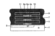
We then proceed, as shown in FIG. 2 c, with the selective lateral etching of the germanium or SiGe alloy layers, through oxidizing chemistry, for instance, as described above. This etching is achieved in such a way that the layers 4, 6, 8 of germanium or SiGe alloy are partly eliminated, but that the central parts 4 a, 6 a, 8 a of those layers above the window 3 a are maintained. An arborescent structure is then formed which includes a central trunk made up of these remaining parts 4 a, 6 a, 8 a from the SiGe layers and of the corresponding parts of polycrystalline silicon layers 5, 7, 9. The parts of the polycrystalline silicon layers 5, 7, 9 extending beyond the trunk, form branches that are separated between each other by hollowings. Likewise, the part of the first polysilicium layer 5 that extends beyond the trunk is separated from the dielectric layer 3 by a hollowing.
The following step, as shown in FIG. 2 d, consists in creating, on the external surface of the arborescent structure, a thin layer of dielectric material 10. This layer of dielectric material can be a layer of oxide that can be the result of thermal oxidation of the structure, for instance, or of the deposit of a layer of dielectric material.
As shown in FIG. 2 d, the formation of the dielectric layer 10 is such that we keep the hollowings separating the polycrystalline silicon layers from each other as well as from the substrate 1.
We then proceed with the coating of the arborescent structure, already covered with a layer of dielectric material 10, with polycrystalline silicon 11, in a way to also fill in the hollowings.
Finally, we complete the structure by forming the necessary contacts over the polycrystalline silicon coating 11.

Claims (14)

1. A semiconductor device comprising:
a semiconductor substrate; and
at least one capacitor adjacent said semiconductor substrate and comprising
alternating layers including at least one germanium layer and at least one polycrystalline silicon layer extending laterally outwardly therefrom defining a tree structure,
a dielectric layer on outer portions of the tree structure, and
an electrical conductor on outer portions of the dielectric layer.
2. A semiconductor device in accordance with claim 1 wherein said at least one germanium layer comprises between 10% and 100% germanium.
3. A semiconductor device in accordance with claim 1 wherein said at least one germanium layer comprises between 25% and 55% germanium.
4. A semiconductor device in accordance with claim 1 wherein said substrate comprises a conductive surface portion, and wherein said alternating layers comprise a first germanium layer contacting said conductive surface portion.
5. A semiconductor device in accordance with claim 4 wherein said conductive surface portion comprises a doped semiconductor surface portion.
6. A semiconductor device in accordance with claim 1 wherein said alternating layers comprise an uppermost polycrystalline silicon layer.
7. A semiconductor device according to claim 1 wherein the at least one polycrystalline silicon layer defines at least one gap with adjacent portions;
and wherein said dielectric layer is relatively thin to preserve the at least one gap.
8. A dynamic random access memory (DRAM) device comprising:
a semiconductor substrate and a plurality of memory cells formed thereon, each memory cell comprising a capacitor;
said capacitor comprising
alternating layers including at least one germanium layer and at least one polycrystalline silicon layer extending laterally outwardly therefrom defining a tree structure,
a dielectric layer on outer portions of the tree structure, and
an electrical conductor on outer portions of the dielectric layer.
9. A DRAM device in accordance with claim 8 wherein said at least one germanium layer comprises between 10% and 100% germanium.
10. A DRAM device in accordance with claim 8 wherein said at least one germanium layer comprises between 25% and 55% germanium.
11. A DRAM device in accordance with claim 8 wherein said semiconductor substrate comprises a conductive surface portion, and wherein said alternating layers comprise a first germanium layer contacting said conductive surface portion.
12. A DRAM device in accordance with claim 11 wherein said conductive surface portion comprises a doped semiconductor surface portion.
13. A DRAM device in accordance with claim 8 wherein said alternating layers comprise an uppermost polycrystalline silicon layer.
14. A DRAM device in accordance with claim 8 wherein the at least one polycrystalline silicon layer defines at least one gap with adjacent portions; and wherein said dielectric layer is relatively thin to preserve the at least one gap.
US10/129,881 1999-11-10 2000-11-10 Method for making a stack of capacitors, in particular for dynamic random access memory [DRAM] Expired - Lifetime US7224015B1 (en)

Applications Claiming Priority (2)

Application Number Priority Date Filing Date Title
FR9914105A FR2800913B1 (en) 1999-11-10 1999-11-10 METHOD FOR MANUFACTURING A CAPACITY STACK, PARTICULARLY FOR DYNAMIC DIRECT ACCESS MEMORIES
PCT/FR2000/003153 WO2001035448A2 (en) 1999-11-10 2000-11-10 Method for making a stack of capacitors, in particular for dynamic ram

Publications (1)

Publication Number Publication Date
US7224015B1 true US7224015B1 (en) 2007-05-29

Family

ID=9551943

Family Applications (1)

Application Number Title Priority Date Filing Date
US10/129,881 Expired - Lifetime US7224015B1 (en) 1999-11-10 2000-11-10 Method for making a stack of capacitors, in particular for dynamic random access memory [DRAM]

Country Status (3)

Country Link
US (1) US7224015B1 (en)
FR (1) FR2800913B1 (en)
WO (1) WO2001035448A2 (en)

Cited By (7)

* Cited by examiner, † Cited by third party
Publication number Priority date Publication date Assignee Title
US20080203506A1 (en) * 2004-12-16 2008-08-28 Sylvain David Capacitive Junction Modulator, Capacitive Junction And Method For Making Same
US20140145303A1 (en) * 2012-11-26 2014-05-29 Samsung Electronics Co., Ltd. Semiconductor device and method of fabricating the same
US20150364611A1 (en) * 2014-06-17 2015-12-17 International Business Machines Corporation Semiconductor devices with semiconductor bodies having interleaved horizontal portions and method of forming the devices
US9391176B2 (en) * 2014-10-23 2016-07-12 Globalfoundries Inc. Multi-gate FETs having corrugated semiconductor stacks and method of forming the same
US10090307B2 (en) 2016-01-21 2018-10-02 International Business Machines Corporation Decoupling capacitor on strain relaxation buffer layer
US10833146B2 (en) * 2019-03-29 2020-11-10 International Business Machines Corporation Horizontal-trench capacitor
US20220181160A1 (en) * 2020-12-09 2022-06-09 Applied Materials, Inc. Methods and apparatus for in-situ protection of etched surfaces

Citations (3)

* Cited by examiner, † Cited by third party
Publication number Priority date Publication date Assignee Title
US5155657A (en) * 1991-10-31 1992-10-13 International Business Machines Corporation High area capacitor formation using material dependent etching
US5622882A (en) * 1994-12-30 1997-04-22 Lsi Logic Corporation Method of making a CMOS dynamic random-access memory (DRAM)
US6127220A (en) * 1998-05-14 2000-10-03 Siemens Aktiengesellschaft Manufacturing method for a capacitor in an integrated storage circuit

Family Cites Families (2)

* Cited by examiner, † Cited by third party
Publication number Priority date Publication date Assignee Title
US5679598A (en) * 1994-12-30 1997-10-21 Lsi Logic Corporation Method of making a CMOS dynamic random-access memory (DRAM)
DE19707977C1 (en) * 1997-02-27 1998-06-10 Siemens Ag Capacitor production especially for DRAM cell array

Patent Citations (3)

* Cited by examiner, † Cited by third party
Publication number Priority date Publication date Assignee Title
US5155657A (en) * 1991-10-31 1992-10-13 International Business Machines Corporation High area capacitor formation using material dependent etching
US5622882A (en) * 1994-12-30 1997-04-22 Lsi Logic Corporation Method of making a CMOS dynamic random-access memory (DRAM)
US6127220A (en) * 1998-05-14 2000-10-03 Siemens Aktiengesellschaft Manufacturing method for a capacitor in an integrated storage circuit

Cited By (11)

* Cited by examiner, † Cited by third party
Publication number Priority date Publication date Assignee Title
US20080203506A1 (en) * 2004-12-16 2008-08-28 Sylvain David Capacitive Junction Modulator, Capacitive Junction And Method For Making Same
US20140145303A1 (en) * 2012-11-26 2014-05-29 Samsung Electronics Co., Ltd. Semiconductor device and method of fabricating the same
US9142610B2 (en) * 2012-11-26 2015-09-22 Samsung Electronics Co., Ltd. Semiconductor device including supporters on a lower electrode thereof and method of fabricating the same
US20150364611A1 (en) * 2014-06-17 2015-12-17 International Business Machines Corporation Semiconductor devices with semiconductor bodies having interleaved horizontal portions and method of forming the devices
US9349880B2 (en) * 2014-06-17 2016-05-24 Globalfoundries Inc. Semiconductor devices with semiconductor bodies having interleaved horizontal portions and method of forming the devices
US9391176B2 (en) * 2014-10-23 2016-07-12 Globalfoundries Inc. Multi-gate FETs having corrugated semiconductor stacks and method of forming the same
US10090307B2 (en) 2016-01-21 2018-10-02 International Business Machines Corporation Decoupling capacitor on strain relaxation buffer layer
US10424585B2 (en) 2016-01-21 2019-09-24 International Business Machines Corporation Decoupling capacitor on strain relaxation buffer layer
US10644007B2 (en) 2016-01-21 2020-05-05 International Business Machines Corporation Decoupling capacitor on strain relaxation buffer layer
US10833146B2 (en) * 2019-03-29 2020-11-10 International Business Machines Corporation Horizontal-trench capacitor
US20220181160A1 (en) * 2020-12-09 2022-06-09 Applied Materials, Inc. Methods and apparatus for in-situ protection of etched surfaces

Also Published As

Publication number Publication date
WO2001035448A3 (en) 2001-10-11
WO2001035448A2 (en) 2001-05-17
FR2800913A1 (en) 2001-05-11
FR2800913B1 (en) 2004-09-03

Similar Documents

Publication Publication Date Title
JP3079021B2 (en) Semiconductor capacitor structure and forming method
US5793076A (en) Scalable high dielectric constant capacitor
US5962885A (en) Method of forming a capacitor and a capacitor construction
US5918118A (en) Dual deposition methods for forming contact metallizations, capacitors, and memory devices
US6800898B2 (en) Integrated circuit configuration and method of fabricating a dram structure with buried bit lines or trench capacitors
US6372574B1 (en) Method of forming a capacitor container electrode and method of patterning a metal layer by selectively silicizing the electrode or metal layer and removing the silicized portion
US6162671A (en) Method of forming capacitors having high dielectric constant material
US20150031212A1 (en) Method for obtaining extreme selectivity of metal nitrides and metal oxides
US7605033B2 (en) Low resistance peripheral local interconnect contacts with selective wet strip of titanium
KR100597958B1 (en) Methods for forming and integrated circuit structures containing enhanced-surface-area conductive layers
KR20050057080A (en) Method for forming conductive material in opening and structure regarding same
US20010023129A1 (en) Semiconductor device and method for providing a contact hole formed in an insulating film
US7224015B1 (en) Method for making a stack of capacitors, in particular for dynamic random access memory [DRAM]
US20040089891A1 (en) Semiconductor device including electrode or the like having opening closed and method of manufacturing the same
US5907774A (en) Corrugated post capacitor and method of fabricating using selective silicon deposition
US5604659A (en) Microelectronic device with centered storage capacitor cavity sized less than feature size
US6143605A (en) Method for making a DRAM capacitor using a double layer of insitu doped polysilicon and undoped amorphous polysilicon with HSG polysilicon
KR20030084350A (en) Method for fabricating capacitor using electro chemical deposition and wet etching
US5953618A (en) Method of forming a capacitor for a semiconductor device
US20010024862A1 (en) Method for forming a lower electrode by using an electroplating method
US5849617A (en) Method for fabricating a nested capacitor
US6818497B2 (en) Method for fabricating capacitor using electrochemical deposition
KR100677769B1 (en) Capacitor and method for fabricating the same
CN113517273B (en) Capacitor array structure, method for manufacturing the same and semiconductor memory device
KR100474989B1 (en) Manufacturing method of capacitor with barrier layer for semiconductor device

Legal Events

Date Code Title Description
AS Assignment

Owner name: STMICROELECTRONICS S.A., FRANCE

Free format text: ASSIGNMENT OF ASSIGNORS INTEREST;ASSIGNORS:SKOTNICKI, THOMAS;ZURCZAK, MALGORZATA;MALLARDEAU, CATHERINE;REEL/FRAME:013416/0512;SIGNING DATES FROM 20020717 TO 20020805

AS Assignment

Owner name: STMICROELECTRONICS S.A., FRANCE

Free format text: CORRECTED COVER SHEET TO CORRECT SPELLING OF THE SECOND ASSIGNOR'S NAME RECORDED AT REEL 013416 FRAME 0512;ASSIGNORS:SKOTNICKI, THOMAS;JURCZAK, MALGORZATA;MALLARDEAU, CATHERINE;REEL/FRAME:013926/0625;SIGNING DATES FROM 20020717 TO 20020805

STCF Information on status: patent grant

Free format text: PATENTED CASE

CC Certificate of correction
FPAY Fee payment

Year of fee payment: 4

FPAY Fee payment

Year of fee payment: 8

MAFP Maintenance fee payment

Free format text: PAYMENT OF MAINTENANCE FEE, 12TH YEAR, LARGE ENTITY (ORIGINAL EVENT CODE: M1553); ENTITY STATUS OF PATENT OWNER: LARGE ENTITY

Year of fee payment: 12