US7173587B2 - Addressing process and device for a bistable liquid crystal screen - Google Patents
Addressing process and device for a bistable liquid crystal screen Download PDFInfo
- Publication number
- US7173587B2 US7173587B2 US10/353,244 US35324403A US7173587B2 US 7173587 B2 US7173587 B2 US 7173587B2 US 35324403 A US35324403 A US 35324403A US 7173587 B2 US7173587 B2 US 7173587B2
- Authority
- US
- United States
- Prior art keywords
- column
- line
- signals
- electrodes
- signal
- Prior art date
- Legal status (The legal status is an assumption and is not a legal conclusion. Google has not performed a legal analysis and makes no representation as to the accuracy of the status listed.)
- Expired - Fee Related, expires
Links
Images


Classifications
-
- G—PHYSICS
- G09—EDUCATION; CRYPTOGRAPHY; DISPLAY; ADVERTISING; SEALS
- G09G—ARRANGEMENTS OR CIRCUITS FOR CONTROL OF INDICATING DEVICES USING STATIC MEANS TO PRESENT VARIABLE INFORMATION
- G09G3/00—Control arrangements or circuits, of interest only in connection with visual indicators other than cathode-ray tubes
- G09G3/20—Control arrangements or circuits, of interest only in connection with visual indicators other than cathode-ray tubes for presentation of an assembly of a number of characters, e.g. a page, by composing the assembly by combination of individual elements arranged in a matrix no fixed position being assigned to or needed to be assigned to the individual characters or partial characters
- G09G3/34—Control arrangements or circuits, of interest only in connection with visual indicators other than cathode-ray tubes for presentation of an assembly of a number of characters, e.g. a page, by composing the assembly by combination of individual elements arranged in a matrix no fixed position being assigned to or needed to be assigned to the individual characters or partial characters by control of light from an independent source
- G09G3/36—Control arrangements or circuits, of interest only in connection with visual indicators other than cathode-ray tubes for presentation of an assembly of a number of characters, e.g. a page, by composing the assembly by combination of individual elements arranged in a matrix no fixed position being assigned to or needed to be assigned to the individual characters or partial characters by control of light from an independent source using liquid crystals
-
- G—PHYSICS
- G02—OPTICS
- G02F—OPTICAL DEVICES OR ARRANGEMENTS FOR THE CONTROL OF LIGHT BY MODIFICATION OF THE OPTICAL PROPERTIES OF THE MEDIA OF THE ELEMENTS INVOLVED THEREIN; NON-LINEAR OPTICS; FREQUENCY-CHANGING OF LIGHT; OPTICAL LOGIC ELEMENTS; OPTICAL ANALOGUE/DIGITAL CONVERTERS
- G02F1/00—Devices or arrangements for the control of the intensity, colour, phase, polarisation or direction of light arriving from an independent light source, e.g. switching, gating or modulating; Non-linear optics
- G02F1/01—Devices or arrangements for the control of the intensity, colour, phase, polarisation or direction of light arriving from an independent light source, e.g. switching, gating or modulating; Non-linear optics for the control of the intensity, phase, polarisation or colour
- G02F1/13—Devices or arrangements for the control of the intensity, colour, phase, polarisation or direction of light arriving from an independent light source, e.g. switching, gating or modulating; Non-linear optics for the control of the intensity, phase, polarisation or colour based on liquid crystals, e.g. single liquid crystal display cells
- G02F1/137—Devices or arrangements for the control of the intensity, colour, phase, polarisation or direction of light arriving from an independent light source, e.g. switching, gating or modulating; Non-linear optics for the control of the intensity, phase, polarisation or colour based on liquid crystals, e.g. single liquid crystal display cells characterised by the electro-optical or magneto-optical effect, e.g. field-induced phase transition, orientation effect, guest-host interaction or dynamic scattering
- G02F1/139—Devices or arrangements for the control of the intensity, colour, phase, polarisation or direction of light arriving from an independent light source, e.g. switching, gating or modulating; Non-linear optics for the control of the intensity, phase, polarisation or colour based on liquid crystals, e.g. single liquid crystal display cells characterised by the electro-optical or magneto-optical effect, e.g. field-induced phase transition, orientation effect, guest-host interaction or dynamic scattering based on orientation effects in which the liquid crystal remains transparent
- G02F1/1391—Bistable or multi-stable liquid crystal cells
-
- G—PHYSICS
- G09—EDUCATION; CRYPTOGRAPHY; DISPLAY; ADVERTISING; SEALS
- G09G—ARRANGEMENTS OR CIRCUITS FOR CONTROL OF INDICATING DEVICES USING STATIC MEANS TO PRESENT VARIABLE INFORMATION
- G09G3/00—Control arrangements or circuits, of interest only in connection with visual indicators other than cathode-ray tubes
- G09G3/20—Control arrangements or circuits, of interest only in connection with visual indicators other than cathode-ray tubes for presentation of an assembly of a number of characters, e.g. a page, by composing the assembly by combination of individual elements arranged in a matrix no fixed position being assigned to or needed to be assigned to the individual characters or partial characters
- G09G3/34—Control arrangements or circuits, of interest only in connection with visual indicators other than cathode-ray tubes for presentation of an assembly of a number of characters, e.g. a page, by composing the assembly by combination of individual elements arranged in a matrix no fixed position being assigned to or needed to be assigned to the individual characters or partial characters by control of light from an independent source
- G09G3/36—Control arrangements or circuits, of interest only in connection with visual indicators other than cathode-ray tubes for presentation of an assembly of a number of characters, e.g. a page, by composing the assembly by combination of individual elements arranged in a matrix no fixed position being assigned to or needed to be assigned to the individual characters or partial characters by control of light from an independent source using liquid crystals
- G09G3/3611—Control of matrices with row and column drivers
- G09G3/3622—Control of matrices with row and column drivers using a passive matrix
- G09G3/3629—Control of matrices with row and column drivers using a passive matrix using liquid crystals having memory effects, e.g. ferroelectric liquid crystals
-
- G—PHYSICS
- G09—EDUCATION; CRYPTOGRAPHY; DISPLAY; ADVERTISING; SEALS
- G09G—ARRANGEMENTS OR CIRCUITS FOR CONTROL OF INDICATING DEVICES USING STATIC MEANS TO PRESENT VARIABLE INFORMATION
- G09G2300/00—Aspects of the constitution of display devices
- G09G2300/04—Structural and physical details of display devices
- G09G2300/0469—Details of the physics of pixel operation
- G09G2300/0478—Details of the physics of pixel operation related to liquid crystal pixels
- G09G2300/0482—Use of memory effects in nematic liquid crystals
- G09G2300/0486—Cholesteric liquid crystals, including chiral-nematic liquid crystals, with transitions between focal conic, planar, and homeotropic states
-
- G—PHYSICS
- G09—EDUCATION; CRYPTOGRAPHY; DISPLAY; ADVERTISING; SEALS
- G09G—ARRANGEMENTS OR CIRCUITS FOR CONTROL OF INDICATING DEVICES USING STATIC MEANS TO PRESENT VARIABLE INFORMATION
- G09G2310/00—Command of the display device
- G09G2310/06—Details of flat display driving waveforms
-
- G—PHYSICS
- G09—EDUCATION; CRYPTOGRAPHY; DISPLAY; ADVERTISING; SEALS
- G09G—ARRANGEMENTS OR CIRCUITS FOR CONTROL OF INDICATING DEVICES USING STATIC MEANS TO PRESENT VARIABLE INFORMATION
- G09G2310/00—Command of the display device
- G09G2310/06—Details of flat display driving waveforms
- G09G2310/066—Waveforms comprising a gently increasing or decreasing portion, e.g. ramp
-
- G—PHYSICS
- G09—EDUCATION; CRYPTOGRAPHY; DISPLAY; ADVERTISING; SEALS
- G09G—ARRANGEMENTS OR CIRCUITS FOR CONTROL OF INDICATING DEVICES USING STATIC MEANS TO PRESENT VARIABLE INFORMATION
- G09G2320/00—Control of display operating conditions
- G09G2320/02—Improving the quality of display appearance
- G09G2320/0209—Crosstalk reduction, i.e. to reduce direct or indirect influences of signals directed to a certain pixel of the displayed image on other pixels of said image, inclusive of influences affecting pixels in different frames or fields or sub-images which constitute a same image, e.g. left and right images of a stereoscopic display
Definitions
- This invention concerns the field of liquid crystal display devices and more specifically a process and device for controlling the switching between two states of a multiplexed bistable nematic display unit.
- the purpose of the invention is to optimise the electronic line and column addressing signals of a multiplexed bistable display unit in order to eliminate visual disruption of an image that has already been memorised, when addressing the screen to display a new image.
- nematic, cholesteric, smectic, ferro-electric, etc. devices can be distinguished.
- a nematic, achiral or chiralised element is used for example, using a chiral doping agent.
- a spontaneously uniform or slightly twisted texture is obtained, whose thread pitch is slightly bigger than a few micrometers.
- the orientation and anchoring of the liquid crystal close to the surfaces are defined by layers or alignment treatments applied to the substrates. In the absence of a field, in this way a uniform or slightly twisted nematic texture is imposed.
- nematic display units twisted nematics (TN), super-twisted nematics (STN, electrically controlled birefringent (ECB), vertically aligned nematics, etc.
- nematic display units are that of bistable, multistable or metastable nematics.
- bistable, multistable or metastable nematics In this case, at least two distinct textures can be created in the cell, with the same anchoring on the surface and stable or metastable in the absence of a field. To switch between the two states, suitable electric signals are applied. Once the image has been registered, it remains in memory in the absence of the field thanks to its bistability.
- This memory of bistable display units is very interesting for many applications. On the one hand, it makes possible a very low image refresh rate, which helps considerably in lowering the consumption of portable devices. On the other hand, for rapid applications (e.g. video), the memory guarantees a very high rate of multiplexing, making high-resolution video possible.
- It is formed of a layer of chiralised or cholerestic nematic liquid crystal between two blades or substrates, of which at least one is transparent.
- Two electrodes respectively positioned on the substrates allow electrical command signals to be applied to the chiralised nematic liquid crystal situated between them.
- anchoring layers direct the liquid crystal molecules to the desired directions.
- the molecule anchoring is strong and slightly angled, on the slave blade it is low and flat. The anchoring of the molecules on these surfaces is monostable.
- An optical system completes the device.
- U and T are stable in the absence of a field.
- the uniform texture may be slightly twisted to favour the device's optics. This is obtained by an angle between the direction of the anchoring on the master blade and on the slave blade.
- the two textures are 180° different and are topologically incompatible.
- the spontaneous pitch p o of the nematic is selected at almost 4 times the thickness D of the cell (p o ⁇ 4d) in order to make the energies of u and T essentially equal. Without a field, there is no other state with a lower energy: U and T have a true bistability.
- the two bistable textures are topologically distinct, it is impossible to transform one into the other by continuous volume distortion.
- the transformation of a U texture into a T texture or vice versa therefore requires rupture of the anchoring on the surfaces, induced by a strong external field, or by moving one of the lines of disinclination.
- This second phenomenon which is much slower than the first, can be neglected and will not be detailed herein.
- Any alignment layer of a liquid crystal can be characterised by a zenithal anchoring energy A z .
- This energy is always finite. It can then be shown that there is a field threshold E C that is also finite (anchoring break threshold), that gives the surface, regardless of the previous texture in the absence of the field, a homeotropic texture (H).
- the breakage of the anchoring requires a field to be applied at least equal to the field threshold E C .
- This field must be applied long enough so that the re-orientation of the liquid crystal close to the surface ends in the homeotropic texture. This minimum time depends on the amplitude of the field applied, as well as the physical characteristics of the liquid crystal and the alignment layer.
- E C A z / ⁇ square root over (K 33 ⁇ O ⁇ ) ⁇ , where A z is the zenithal anchoring energy, K 33 the elastic twisting coefficient of the liquid crystal, ⁇ its relative dielectric anisotropy and ⁇ o the dielectric constant of the vacuum.
- V c E C .d, where d is the thickness of the liquid crystal cell.
- the anchoring is considered to be broken when the molecules are perpendicular to the blade next to this surface, and when the return tension exerted by the surface on these molecules is nil.
- the nematic molecules close to the broken surface are in an unstable equilibrium when the electrical field is cut off, and may either return to their initial orientation, or turn in the opposite direction and induce a new texture, different from the initial texture by a twist of 180°.
- the control of the final texture depends on the form of the electrical signal applied, and in particular the way in which this field is brought to zero.
- the switching of the strong surface in such a short space of time induces high flow close to this surface, which spreads throughout the volume and reaches the weak surface (slave blade) after a characteristic time of less than a micro-second.
- the shearing force induced on the weak surface (slave blade) creates a hydrodynamic force on the molecules of this surface. This force is in the opposite direction to the elastic force induced by the angle of the master blade.
- the shear force is strong enough, the hydrodynamic force on the weak surface is stronger, it favours the twisted texture T.
- the elastic force on the weak surface is weaker and it induces the uniform texture U.
- the direction of rotation of the molecules in the cell is indicated by an arrow on FIG. 1 .
- the volume is then re-orientated, with a characteristic relax time t vol equal to ⁇ 1 d 2 /K, where d is the thickness of the cell. This time is significantly greater than the relax time of the strong surface, typically around one millisecond.
- a pulse must be applied to it, providing a field greater than the anchoring breakage field of the slave blade and then wait the time required for the pixels in the molecule to change.
- the breakage field depends on the elastic and electrical properties of the liquid crystal material and its interaction with the anchoring layer deposited on the slave blade of the cell. It is around a couple of volts to about ten volts per micron.
- the time for the molecules to change is proportional to the rotational viscosity, ⁇ , and inversely proportional to the dielectrical anisotropy of the material used and the square of the field applied. In practice, this time can be as low as a few micro-seconds for fields of 20 volts per micron.
- the pulse includes a first sequence of a duration ⁇ 1 , of an amplitude P 1 such that P 1 >V C followed by a second sequence of a duration ⁇ 2 , and an amplitude P 2 slightly smaller than P 1 such that P 2 >V C and P 2 > ⁇ V, the said second sequence dropping swiftly to zero.
- the pulse includes a first sequence of a duration ⁇ 1 , of an amplitude P 1 >V C followed by a second sequence of a duration ⁇ 2 , and an amplitude P 2 such that P 2 ⁇ V C and: P 1 ⁇ P 2 > ⁇ V.
- Document (1) shows two embodiments of this “slow drop”, shown diagrammatically in FIGS. 2 b 1 and 2 b 2 : the “erase” is either a pulse of duration ⁇ 1 , and amplitude P 1 followed by a slope of duration ⁇ 2 whose drop time is three times greater than the duration of the pulse ( FIG. 2 b 1 ), or a stepped drop, in the form of a signal with two plateaux (first sequence of duration ⁇ 1 and amplitude P 1 , followed by a second sequence of duration ⁇ 2 and amplitude P 2 such that either P 2 >V C and P 2 ⁇ V, or P 2 ⁇ V C and P 1 ⁇ P 2 ⁇ V.
- the stepped drop is easier to carry out with digital electronic equipment, so we will not discuss the slope drop here. However, we can imagine a drop with more than two plateaux.
- the characteristic pulse forms for the change from one texture to another are given in FIG. 2 (see document 1) and document (2).
- the duration and values of the plateaux (P 1 , ⁇ 1 ) and (P 2 , ⁇ 2 ) have been determined experimentally in the examples given below.
- the column signals are applied at the same time to all of the pixels of the line.
- This method allows an image to be addressed in a total time equal to the addressing time of a line multiplied by the number of lines n.
- m+n connections are required to address a screen of m ⁇ n pixels, where m is the number of columns of the matrix in question.
- a multiplexed dot display screen is illustrated in FIG. 3 .
- the electrical signal seen by the pixel is the difference between the signal applied to the line and the signal applied to the column of which the pixel is the intersection.
- This principle of screen is called a “passive screen”. It does not have any active elements allowing it to isolate the pixels.
- a line electrode is common to all of the pixels of the line, and a column electrode is common to all of the pixels of the column, with no active element (e.g. a transistor) .
- the passive screens are consequently easier to manufacture than active screens that have a transistor or a control diode per pixel.
- the final state of the liquid crystal molecules which is to say the optical transmission of the pixel, is determined by the rms value of the voltage applied during the time that the image is addressed.
- the consequence is the limiting of the number of lines of the screen expressed by the criterion of Alt and Plesko (document 3).
- the BiNem screens considered are also formed by n ⁇ m pixels ( FIG. 3 ), carried out at the intersections of perpendicular conductive strips on the two substrates already mentioned.
- the pixel of line N+1, column M is shown in black.
- the device is completed by connections and circuits placed on the substrate or on auxiliary boards.
- the write and erase signals applied to the pixels are created by the combination of line and column signals. They permit writing and erasing to be performed line by line, and thus rapidly of the screens in question.
- the voltage applied to the pixel during the line write time must be equal to the pulse, which, upon demand, either stops swiftly causing a voltage drop greater than or equal to ⁇ V and creates the T twisted texture (usually an optically black state), or drops progressively by plateaux and creates the U uniform texture (usually an optically shiny state).
- the possibility of changing between the U and T textures and reciprocally by multiplexing is shown by the electro-optical curve shown in FIG. 4 : the BiNem pixel is addressed with a double plateau pulse of value P 1 fixed and P 2 variable.
- the pulse times are 0.8 ms. Taking account of the orientation of the polarisers in this example, a minimum transmission corresponds to the T state and a maximum to the U state.
- the voltage drop value ⁇ V required to write is equal to approximately 6V and the break voltage V C approximately 5V.
- F 1 and F 2 are defined as the two operating points located at the point of inflection where the optical transmission curve rises or falls shown in FIG. 4 .
- the voltage corresponding to point F 2 may correspond to the value of the second plateau A 2 of the line signal.
- FIG. 6 shows the principle of line and column signals carrying out the write and erase functions, when the selection is on the operating point F 2 as described above.
- the line signal ( FIG. 6 a ) has two plateaux: the first provides the A 1 voltage during ⁇ 1 , the second A 2 during ⁇ 2 .
- the column signal ( FIGS. 6 b and 6 c ) of amplitude C is only applied during the time ⁇ 2 , positively or negatively according on whether writing or erasing is to be carried out.
- the time ⁇ 3 separates two line pulses.
- FIGS. 6 d and 6 e show the signals applied respectively to the terminals of an erased pixel and to the terminals of a written pixel. These signals are very simple and permit easy adjustment of all their parameters to suit the characteristics of the screen.
- FIGS. 7 , 8 and 9 show techniques that permit the principle signals of FIG. 6 to be transformed into symmetrical signals with a nil mean value.
- FIG. 7 two identical signals with opposite polarities that follow one another form the line selection signal.
- FIGS. 7 a , 7 b , 7 c , 7 d and 7 e respectively represent the line signals, the column erase signals, the column write signals, the erase signals at the terminals of a pixel.
- FIG. 8 Another symmetrisation technique is proposed in FIG. 8 .
- the signals are the same as that on FIG. 5 . However, their signs are inverted at each change of image.
- the line signal driver must, in the previous cases and due to the symmetrisation, supply a voltage of +/ ⁇ A 1 which is to say a total excursion of 2.A 1 .
- a notable simplification of the divers can be obtained if the maximum excursion is reduced to a value below 2.A 1 .
- FIGS. 9 a , 9 b , 9 c , 9 d and 9 e respectively show the line signals, erase column signals, write column signals, erase signals to the terminals of a pixel and write signals to the terminals of a pixel.
- the classic method of multiplexing the BiNem can limit the optical performances of the images displayed.
- the pixel signal is composed of two contributions: the signal resulting from the line and column signals during the period in which its line is selected, plus parasite signals that correspond to the column signals applied to the pixel outside of the period in which its line is selected.
- FIG. 10 shows the existence of these parasite signals.
- FIGS. 10 a , 10 b , 10 c , 10 d and 10 e respectively show the line signals, erase column signals, write column signals, erase signals to the terminals of a pixel and write signals to the terminals of a pixel.
- FIG. 10 f shows a dot matrix screen.
- the amplitude of the column signals is much lower than the anchoring breakage threshold.
- the parasite signals cannot in any case cause the textures to change. Nevertheless, they cause temporary disruptions to the optical response by deforming the texture of the pixel without breaking either the strong or weak anchoring. The optical appearance may be severely disrupted during the total duration of the addressing of the screen. This may cause for example dither, a loss of image contrast, etc. After all of the image has been written, the parasite voltages disappear and the pixels return to their initial, stable texture until the next addressing cycle.
- ⁇ CL is the characteristic response time of the liquid crystal for column pulses of amplitude C.
- the integration time to be taken into consideration is the shortest, i.e. equal to the response time of the liquid crystal.
- the criterion to be respected is in this case more severe. We will then look to position it at ⁇ 1 + ⁇ 2 + ⁇ 3 ⁇ CL .
- a first method is to minimise C.
- the lower limit of C is imposed by the electro-optical response curve shown in FIG. 4 . Too low of a value for C will not allow the change to be made between two textures.
- Criterion 1 is not respected.
- ⁇ CL ( ⁇ d 2 /K ⁇ 2 )/[(V/V F ) 2 ⁇ 1]
- ⁇ is the rotational viscosity and k the elastic constant of the liquid crystal.
- k the elastic constant of the liquid crystal.
- d is the thickness of the cell typically 1.5 *m and V the C column voltage typically 2 V.
- the inventors propose a new process to eliminate the dither effect. It involves modifying the column signal so as to reduce the Vrms value with respect to the classic case, while continuing to synchronise its drop with that of the line pulse.
- the addressing process of a bistable nematic anchoring breakage liquid crystal dot matrix screen is characterised by the fact that that it comprises at least the step consisting of applying, to the electrodes of the screen column, an electrical signal whose parameters are adapted to reduce the mean quadratic voltage of the parasite pixel pulses to a value lower than the Fréederickzs voltage, in order to reduce the parasitic optical effects of addressing.
- the first variant consists of reducing the time ⁇ C during which the column signal is applied, this time becoming less than to the time ⁇ 2 of the duration of the second plateau of the line signal.
- the second variant proposed consists of changing the form of the column signal so that the effective voltage is reduced.
- This invention also proposes a dot matrix screen addressing device.
- FIG. 1 shows diagrammatically the state of the technique and more precisely a pixel of the liquid crystal cell and, in this pixel, the two stable textures without the applied molecule field: (called U uniform texture and T twisted texture).
- the diagram H shows the texture of the molecules in the field.
- the arrows indicate the rotation of the molecules when the field is stopped.
- FIG. 2 shows the classic pixel signals allowing the switch between the two textures.
- the time for the write signal to drop is less than one tenth of its duration or less than 50 micro seconds in the case of long pulses.
- Two erase signals are proposed: one is a pulse followed by a slope whose drop time is greater than three times the duration of the pulse, the other is a stepped drop, a signal with two plateaux.
- FIG. 3 shows the principle of a classic multiplexed dot matrix screen.
- the active zone of a pixel is situated at the intersection of the column and line electrodes.
- the column signals are applied simultaneously to all of the columns, then it moves the following line.
- FIG. 4 provides an example of an electro-optical curve of a liquid crystal pixel operating according to the classic principle of FIG. 1 .
- the first plateau of the applied voltage is equal to 16 V, and the optical transmission depends on the value of the second plateau.
- FIG. 5 details the correspondence between the value of the second plateau and the texture obtained in a classic device.
- the U uniform texture is obtained for a second plateau value of between 5V and 9V.
- the T twisted texture is obtained for a second plateau value of between 0 and 5V or between 9 V and 16V.
- FIG. 6 illustrates the line and column signals of classic multiplexed addressing: either one or the other of the two textures is obtained depending on the column signal sign.
- FIG. 7 shows a classic improvement proposed to avoid polarisation of the liquid crystal cell which could lead to slow damage of the material by electrolysis.
- the line and column signals are symmetrised, their mean value is hence nil.
- FIG. 8 presents another classic version where the symmetry is obtained by inverting the polarity from one image to the other.
- FIG. 9 presents the signals that allow symmetrical signals to be applied to the pixels, while minimising the control circuit voltage excursion.
- the lines not selected receive a line signal equal to the means of the column signals instead of not receiving a signal, as in the previous cases.
- FIG. 10 shows the existence of parasite signals at the pixel terminals, known to come from the column signals picked up by the pixel when its line is not active.
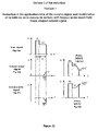
- FIG. 11 shows a variant of a new form of signals and circuitry for generating the signals, according to the invention, proposed by the inventors.
- the column pulse lasts for a shorter time than the duration of the second plateau of the line signal and has a toothed form whose drop is synchronised with the drop of the second plateau of the line signal.
- FIG. 12 shows another variant of the new form of signals, according to the invention, proposed by the inventors.
- the column pulse lasts for a shorter time than the duration of the second plateau of the line signal and has a slope form whose drop is synchronised with the drop of the second plateau of the line signal.
- FIG. 13 shows another variant of the new form of signals, according to the invention, proposed by the inventors.
- the column pulse lasts for a shorter time than the duration of the second plateau of the line signal and has a double plateau form whose drop is synchronised with the drop of the second plateau of the line signal.
- FIG. 14 describes, by way of example, the optical signal of a pixel in the white state when the lines apart from its line are addressed.
- This pixel is sensitive to the parasite column signals. Its optical transmission depends on the column pulse for applied.
- 3 cases are shown: a classic case ( FIG. 14 a ), a tooth shaped column signal that is shorter than the second plateau of the line signal ( FIG. 14 b , in accordance with the invention), a column signal shorter than the second plateau of the line signal and with a slope form ( FIG. 14 c , in accordance with the invention).
- a classic case FIG. 14 a
- a tooth shaped column signal that is shorter than the second plateau of the line signal FIG. 14 b
- FIG. 14 c in accordance with the invention.
- This invention applies in particular to the BiNem devices described in document 1 using two textures, one of which is uniform or slightly twisted and in which the molecules are at least virtually parallel to one another, and the other which differs from the first by a twist of around +/ ⁇ 180°.
- the new column signal C′ is applied for a time ⁇ 0 ⁇ 2 , keeping the amplitude of C′ about the same as that of C, as an increase of C′ would increase the rms value of the parasite voltage applied to the pixels, and a reduction in C′ would no longer allow switching to take place due to the limit indicated by the electro-optical curve of FIG. 4 .
- the signals corresponding to variant 1 are shown in FIGS. 11 a – 11 e of FIG. 11 . Above FIGS. 11 a – 11 e , circuitry for generating the signals is shown.
- the circuitry includes six vertical columns of column electrodes 110 , and six horizontal lines of line electrodes 120 .
- a signal applicator 100 applies column signals to column electrodes 110 and line signals to line electrodes 120 .
- FIG. 11 a a line signal
- FIG. 11 b an erase column signal
- FIG. 11 c a write column signal
- FIG. 11 d a pixel erase signal
- FIG. 11 e a pixel write signal.
- Vrms 2 ⁇ C C′ 2 /( ⁇ 1 + ⁇ 2 )
- the line signal illustrated in FIG. 11 a includes a first sequence of duration ⁇ 1 and amplitude A 1 followed by a second sequence of duration ⁇ 2 (greater than ⁇ 1 ) and of amplitude A 2 (less than A 1 ) .
- the slopes where these two sequences rise and fall are virtually vertical.
- the erase column signal illustrated in FIG. 11 b includes a pulse of duration ⁇ C and amplitude C′ of the same polarity as the line signal illustrated in FIG. 11 a .
- the slopes where these two sequences rise and fall are virtually vertical.
- the duration ⁇ C is around half the duration of the duration ⁇ 2 .
- the descending slope of the erase column signal is synchronised with the descending slope of the line signal.
- the write column signal illustrated in FIG. 11 c is distinguished from the erase column signal illustrated in FIG. 11 b by an inversion of the polarity.
- ⁇ C and amplitude C′ we can find a pulse of duration ⁇ C and amplitude C′, with vertical rising and descending slopes, the descending slope being synchronised with the descending slope of the line signal.
- the voltage present at the terminals of the pixel as part of a erase operation, illustrated in FIG. 11 d includes a series of three teeth with vertical rising and descending slopes.
- the first step of amplitude A 1 lasts ⁇ 1 .
- the second step of amplitude A 2 lasts ⁇ 2 ⁇ C .
- the third step of amplitude A 2 ⁇ C′ lasts ⁇ C .
- the voltage present at the terminals of the pixel as part of a write operation, illustrated in FIG. 11 e also includes a series of three successive steps, with vertical rising and descending slopes: a first step of duration ⁇ 1 and amplitude A 1 , a second step of amplitude A 2 and duration ⁇ 2 ⁇ C , and a third step of amplitude A 2 +C′ and duration ⁇ C .
- the intermediate step has an amplitude between the initial amplitude A 1 , the strongest, and the final amplitude A 2 ⁇ C′, the weakest, whereas in the case of a pixel being written, the intermediate amplitude A 2 is smaller than the initial amplitude, which is the strongest, A 1 , and the final amplitude A 2 +C′.
- the form of the column signal is modified so as to reduce its effective voltage with respect to that of a standard column signal composed of rectangular pulses.
- the duration of the column signal may also be reduced with respect to a classic ⁇ 2 , in order to benefit from the advantages of variant 1.
- the maximum value of the column signal C′′ may be increased with respect to the classic value of C, which permits switching between the two textures (see electro-optical curve of FIG. 4 ).
- FIG. 12 An example of signals corresponding to example 1 of variant 2 is given in FIG. 12 .
- FIG. 12 a we find: a line signal, FIG. 12 b : an erase column signal, FIG. 12 c : a write column signal, FIG. 12 d : an erase pixel signal, and FIG. 12 e : a write pixel signal.
- the column pulse has a duration of ⁇ C and the form of a slope of maximum C′′.
- Vrms2 ⁇ C C′′ 2/3( ⁇ 1 + ⁇ 2 )
- the signal illustrated in FIG. 12 a includes a sequence of duration ⁇ 1 and amplitude A 1 followed by a second sequence of duration ⁇ 2 (greater than ⁇ 1 ) and amplitude A 2 (smaller than A 1 ).
- the slopes where these two sequences rise and fall are virtually vertical.
- the erase column signal illustrated in FIG. 12 b includes a pulse of duration ⁇ C with a linearly rising slope which reaches the amplitude C′ and a vertical descending slope.
- the write column signal illustrated in FIG. 12 c is distinguished from the erase column signal illustrated in FIG. 12 b by an inversion of polarity. We an thus see in FIG. 12 c a pulse of duration ⁇ C with a linearly rising slope that reaches the amplitude C′ and a vertically descending slope.
- the voltage present at the terminals of the pixel being erased has three successive sequences: a first sequence of amplitude A1 and duration ⁇ 1 , a second sequence of amplitude A 2 and duration ⁇ 2 ⁇ C , and a third sequence with a progressively decreasing amplitude of duration ⁇ C , passing from an initial amplitude A 2 to a final amplitude A 2 ⁇ C′.
- the A 2 value for FIG. 12 d is an intermediate value.
- the voltage present at the terminals of the pixel being written also has three successive sequences: a first sequence A 1 of amplitude A 1 and duration ⁇ 1 , a second sequence of amplitude A 2 and duration ⁇ 2 ⁇ C , and a third sequence with a progressively increasing amplitude of duration ⁇ C , passing from an initial amplitude A 2 to a higher value of A 2 +C′.
- the A 2 value is an intermediate value.
- FIG. 13 An example of signals corresponding to example 2 of variant 2 is given in FIG. 13 .
- FIG. 13 a a line signal
- FIG. 13 b an erase column signal
- FIG. 13 c a write column signal
- FIG. 13 d an erase pixel signal
- FIG. 13 a write pixel signal.
- the optical transmission of a pixel of a BiNem screen during the addressing of an image was measured. Due to the arrangement of the polarisers, the uniform texture given in this case was the white optic state, and the texture written was the black state. When the line of the pixel is addressed, the pixel is changed to a uniform texture (white state) and then it is subjected to parasite column signals for the rest of the image addressing. The optical transmission will then drop to an intermediate value between the black and the white values. The optical response is measured for the three following cases:
- FIG. 14 It can be observed in FIG. 14 that the optical transmission level is very disrupted (close to black) in this classic case ( FIG. 14 a ) .
- This case corresponds to a marked dither of the screen during its electrical addressing.
- FIG. 14 b the optical state is less disrupted but remains grey. The dither is still visible.
- FIG. 14 c an optical state very close to white is measured. The optical state of the pixel measured is hardly disrupted by the parasite column signals.
- the inventors present a method that allows the switching between the two states of the pixels of a bistable liquid crystal dot matrix passive screen switching by surface breakage to be controlled.
- the original signals proposed use a line signal with two plateaux, and a column signal that is retarded with respect to the start and ending exactly at the end of the second plateaux of the line signal and of varied form, either classic tooth shaped or for example a slope.
- This method allows either rapid drop signals, to permit the twisted state to be obtained, or a slow drop with three plateaux to obtain the uniform state, to be applied simultaneously to the screen pixels.
- the invention reduces and in some cases even eliminates the parasitic effects when the image is changing and on the other hand makes switching easier by making the erase signal form closer to that of a slowly decreasing curve.
Landscapes
- Physics & Mathematics (AREA)
- Engineering & Computer Science (AREA)
- Chemical & Material Sciences (AREA)
- Crystallography & Structural Chemistry (AREA)
- General Physics & Mathematics (AREA)
- Nonlinear Science (AREA)
- Computer Hardware Design (AREA)
- Theoretical Computer Science (AREA)
- Optics & Photonics (AREA)
- Liquid Crystal (AREA)
- Liquid Crystal Display Device Control (AREA)
- Control Of Indicators Other Than Cathode Ray Tubes (AREA)
Applications Claiming Priority (2)
| Application Number | Priority Date | Filing Date | Title |
|---|---|---|---|
| FR0201448A FR2835644B1 (fr) | 2002-02-06 | 2002-02-06 | Procede et dispositif d'adressage d'un ecran cristal liquide bistable |
| FR0201448 | 2002-02-06 |
Publications (2)
| Publication Number | Publication Date |
|---|---|
| US20030146894A1 US20030146894A1 (en) | 2003-08-07 |
| US7173587B2 true US7173587B2 (en) | 2007-02-06 |
Family
ID=27589601
Family Applications (1)
| Application Number | Title | Priority Date | Filing Date |
|---|---|---|---|
| US10/353,244 Expired - Fee Related US7173587B2 (en) | 2002-02-06 | 2003-01-27 | Addressing process and device for a bistable liquid crystal screen |
Country Status (8)
| Country | Link |
|---|---|
| US (1) | US7173587B2 (fr) |
| EP (1) | EP1335348A1 (fr) |
| JP (1) | JP4387113B2 (fr) |
| KR (1) | KR100952030B1 (fr) |
| CN (1) | CN1290075C (fr) |
| CA (1) | CA2418312C (fr) |
| FR (1) | FR2835644B1 (fr) |
| TW (1) | TWI310538B (fr) |
Cited By (3)
| Publication number | Priority date | Publication date | Assignee | Title |
|---|---|---|---|---|
| US20060022919A1 (en) * | 2002-11-26 | 2006-02-02 | Philippe Martinot-Lagarde | Bistable nematic liquid crystal display device and method for controlling such a device |
| EP2178079A1 (fr) | 2008-10-15 | 2010-04-21 | Nemoptic | Procédé économique en énergie pour marquer une zone d'un écran à cristal liquide |
| US8487856B2 (en) | 2006-04-07 | 2013-07-16 | Nemoptic | Addressing method for a bistable nematic liquid crystal matrix screen with regulated average quadratic voltage |
Families Citing this family (10)
| Publication number | Priority date | Publication date | Assignee | Title |
|---|---|---|---|---|
| FR2838858B1 (fr) | 2002-04-19 | 2004-08-27 | Nemoptic | Dispositif d'affichage bistable a cristaux liquides comprenant des moyens d'adressage perfectionnes |
| TWI296731B (en) * | 2004-12-24 | 2008-05-11 | Au Optronics Corp | A pixel structure, a liquid crystal panel, a method for improving color shift event of liquid crystal panel, and a method for fabricating a low color shift liquid crystal panel |
| CN100447853C (zh) * | 2005-10-14 | 2008-12-31 | 财团法人工业技术研究院 | 双稳态对掌性向列型液晶显示器的灰阶驱动方法以及连续更新画面的方法 |
| FR2916295B1 (fr) * | 2007-05-18 | 2010-03-26 | Nemoptic | Procede d'adressage d'un ecran matriciel a cristal liquide et dispositif appliquant ce procede |
| JP5432149B2 (ja) * | 2008-08-19 | 2014-03-05 | セイコーインスツル株式会社 | 双安定ネマチックのドットマトリクス液晶ディスプレイの駆動方法および駆動デバイス |
| JP5421658B2 (ja) * | 2009-05-29 | 2014-02-19 | セイコーインスツル株式会社 | 双安定ネマチックのドットマトリクス液晶表示パネルの駆動方法及び駆動デバイス |
| CN102208175B (zh) * | 2010-03-29 | 2016-01-20 | 精工电子有限公司 | 双稳定型液晶显示装置的驱动方法 |
| JP5341826B2 (ja) | 2010-06-18 | 2013-11-13 | セイコーインスツル株式会社 | 双安定液晶表示パネルの駆動方法及び駆動デバイス |
| US10558065B2 (en) * | 2018-04-13 | 2020-02-11 | Kent Displays Inc. | Liquid crystal writing device with slow discharge erase |
| CN109272952A (zh) * | 2018-10-22 | 2019-01-25 | 信利半导体有限公司 | 双稳态液晶的驱动方法及装置和双稳态液晶设备 |
Citations (6)
| Publication number | Priority date | Publication date | Assignee | Title |
|---|---|---|---|---|
| US5594464A (en) * | 1992-05-07 | 1997-01-14 | Seiko Epson Corporation | Liquid crystal display device having two metastable states and driving method therefor |
| FR2740894A1 (fr) | 1995-11-08 | 1997-05-09 | Centre Nat Rech Scient | Dispositif d'affichage perfectionne a base de cristaux liquides et a effet bistable |
| US6252571B1 (en) * | 1995-05-17 | 2001-06-26 | Seiko Epson Corporation | Liquid crystal display device and its drive method and the drive circuit and power supply circuit device used therein |
| US20020084961A1 (en) * | 2000-09-23 | 2002-07-04 | Acosta Elizabeth Jane | Liquid crystal display device and a method of operating a liquid crystal display device |
| US6452573B1 (en) * | 1997-05-07 | 2002-09-17 | Nemoptic, S.A. | Liquid crystal device comprising anchoring means on at least one confinement plate providing a degenerated orientation |
| US6784968B1 (en) * | 1999-03-03 | 2004-08-31 | Zbd Displays Limited | Addressing bistable nematic liquid crystal devices |
Family Cites Families (2)
| Publication number | Priority date | Publication date | Assignee | Title |
|---|---|---|---|---|
| JP3555578B2 (ja) * | 1993-02-25 | 2004-08-18 | セイコーエプソン株式会社 | 液晶表示装置の駆動方法 |
| GB9510612D0 (en) * | 1995-05-25 | 1995-07-19 | Central Research Lab Ltd | Improvements in or relating to the addressing of liquid crystal displays |
-
2002
- 2002-02-06 FR FR0201448A patent/FR2835644B1/fr not_active Expired - Fee Related
-
2003
- 2003-01-27 US US10/353,244 patent/US7173587B2/en not_active Expired - Fee Related
- 2003-01-30 CN CNB031019730A patent/CN1290075C/zh not_active Expired - Fee Related
- 2003-01-30 TW TW092102090A patent/TWI310538B/zh not_active IP Right Cessation
- 2003-02-03 CA CA002418312A patent/CA2418312C/fr not_active Expired - Fee Related
- 2003-02-04 EP EP03290272A patent/EP1335348A1/fr not_active Withdrawn
- 2003-02-06 JP JP2003029639A patent/JP4387113B2/ja not_active Expired - Fee Related
- 2003-02-06 KR KR1020030007428A patent/KR100952030B1/ko not_active IP Right Cessation
Patent Citations (7)
| Publication number | Priority date | Publication date | Assignee | Title |
|---|---|---|---|---|
| US5594464A (en) * | 1992-05-07 | 1997-01-14 | Seiko Epson Corporation | Liquid crystal display device having two metastable states and driving method therefor |
| US5900852A (en) * | 1992-05-07 | 1999-05-04 | Seiko Epson Corporation | Liquid crystal display device having two metastable states and driving method therefor |
| US6252571B1 (en) * | 1995-05-17 | 2001-06-26 | Seiko Epson Corporation | Liquid crystal display device and its drive method and the drive circuit and power supply circuit device used therein |
| FR2740894A1 (fr) | 1995-11-08 | 1997-05-09 | Centre Nat Rech Scient | Dispositif d'affichage perfectionne a base de cristaux liquides et a effet bistable |
| US6452573B1 (en) * | 1997-05-07 | 2002-09-17 | Nemoptic, S.A. | Liquid crystal device comprising anchoring means on at least one confinement plate providing a degenerated orientation |
| US6784968B1 (en) * | 1999-03-03 | 2004-08-31 | Zbd Displays Limited | Addressing bistable nematic liquid crystal devices |
| US20020084961A1 (en) * | 2000-09-23 | 2002-07-04 | Acosta Elizabeth Jane | Liquid crystal display device and a method of operating a liquid crystal display device |
Non-Patent Citations (3)
| Title |
|---|
| "Scanning Limitations of Liquid-Crystal Displays", P. Alt, et al., IEEE Transaction on Electron Devices, vol. ED-21, No. 2, Feb. 1974, pgs 146-155. |
| "Write and erase mechanism of surface controlled bistable Nematic pixel", Giocondo, et al., The European Physical Journal Applied Physics, 3 pages, 1999. |
| Recent Improvements of Bistable Nematic Displays Switched By Anchoring Breaking (BiNem), I. Dozov, et al., SID 01 Digest 2001 SID, pp. 224-227. |
Cited By (4)
| Publication number | Priority date | Publication date | Assignee | Title |
|---|---|---|---|---|
| US20060022919A1 (en) * | 2002-11-26 | 2006-02-02 | Philippe Martinot-Lagarde | Bistable nematic liquid crystal display device and method for controlling such a device |
| US7864148B2 (en) * | 2002-11-26 | 2011-01-04 | Nemoptic | Bistable nematic liquid crystal display device and method for controlling such a device |
| US8487856B2 (en) | 2006-04-07 | 2013-07-16 | Nemoptic | Addressing method for a bistable nematic liquid crystal matrix screen with regulated average quadratic voltage |
| EP2178079A1 (fr) | 2008-10-15 | 2010-04-21 | Nemoptic | Procédé économique en énergie pour marquer une zone d'un écran à cristal liquide |
Also Published As
| Publication number | Publication date |
|---|---|
| KR100952030B1 (ko) | 2010-04-08 |
| CN1437181A (zh) | 2003-08-20 |
| TW200303518A (en) | 2003-09-01 |
| CA2418312C (fr) | 2009-04-28 |
| JP4387113B2 (ja) | 2009-12-16 |
| CN1290075C (zh) | 2006-12-13 |
| TWI310538B (en) | 2009-06-01 |
| FR2835644A1 (fr) | 2003-08-08 |
| JP2004004552A (ja) | 2004-01-08 |
| US20030146894A1 (en) | 2003-08-07 |
| CA2418312A1 (fr) | 2003-08-06 |
| FR2835644B1 (fr) | 2005-04-29 |
| KR20030067543A (ko) | 2003-08-14 |
| EP1335348A1 (fr) | 2003-08-13 |
Similar Documents
| Publication | Publication Date | Title |
|---|---|---|
| US20040141107A1 (en) | Liquid crystal device | |
| KR100372986B1 (ko) | 액정 표시 장치 구동 방법 및 액정 표시 장치 | |
| US7173587B2 (en) | Addressing process and device for a bistable liquid crystal screen | |
| GB2324899A (en) | Active matrix display | |
| JP5148048B2 (ja) | 双安定ネマチック液晶ディスプレイ装置およびこのような装置の制御方法 | |
| KR20020095167A (ko) | 쌍안정 키랄 네마틱 액정 디스플레이와 이러한디스플레이의 구동 방법 | |
| US7724221B2 (en) | Bistable nematic liquid crystal display method and device | |
| US6351256B1 (en) | Addressing method and apparatus | |
| JP4740860B2 (ja) | 双安定ネマティック液晶表示を有する先進的方法および装置 | |
| KR20040066132A (ko) | 액정 디스플레이 디바이스 | |
| KR19990008127A (ko) | 액정 디스플레이 장치 | |
| EP0809232A2 (fr) | Circuit et méthode de commande pour dispositif à cristaux liquides | |
| US20130169898A1 (en) | Method of driving bi-stable liquid crystal panel and driving device | |
| US7352346B2 (en) | Bistable liquid crystal display device including improved addressing means | |
| JPH05303076A (ja) | 液晶装置 | |
| JP5701104B2 (ja) | 双安定型液晶表示装置の駆動方法 | |
| KR20090115965A (ko) | 개선된 스위칭 수단을 포함하는 액정 디스플레이 | |
| JP3093511B2 (ja) | 表示装置 | |
| KR100322448B1 (ko) | 리셋전압과 선택전압의 전압레벨이 같은 주사신호를 인가하는 액정표시장치 | |
| JPH0448366B2 (fr) | ||
| Aristov et al. | Features of the control of array-type liquid-crystal memory displays | |
| JPH0579968B2 (fr) |
Legal Events
| Date | Code | Title | Description |
|---|---|---|---|
| AS | Assignment |
Owner name: NEMOPTIC, FRANCE Free format text: ASSIGNMENT OF ASSIGNORS INTEREST;ASSIGNORS:ANGELE, JACQUES;VERCELLETTO, ROMAIN;ELBHAR, THIERRY;REEL/FRAME:013958/0478 Effective date: 20030210 |
|
| FEPP | Fee payment procedure |
Free format text: PAYOR NUMBER ASSIGNED (ORIGINAL EVENT CODE: ASPN); ENTITY STATUS OF PATENT OWNER: LARGE ENTITY |
|
| FPAY | Fee payment |
Year of fee payment: 4 |
|
| REMI | Maintenance fee reminder mailed | ||
| LAPS | Lapse for failure to pay maintenance fees | ||
| STCH | Information on status: patent discontinuation |
Free format text: PATENT EXPIRED DUE TO NONPAYMENT OF MAINTENANCE FEES UNDER 37 CFR 1.362 |
|
| FP | Lapsed due to failure to pay maintenance fee |
Effective date: 20150206 |