EP0809232A2 - Circuit et méthode de commande pour dispositif à cristaux liquides - Google Patents
Circuit et méthode de commande pour dispositif à cristaux liquides Download PDFInfo
- Publication number
- EP0809232A2 EP0809232A2 EP97303366A EP97303366A EP0809232A2 EP 0809232 A2 EP0809232 A2 EP 0809232A2 EP 97303366 A EP97303366 A EP 97303366A EP 97303366 A EP97303366 A EP 97303366A EP 0809232 A2 EP0809232 A2 EP 0809232A2
- Authority
- EP
- European Patent Office
- Prior art keywords
- signal
- liquid crystal
- switching
- applying
- crystal device
- Prior art date
- Legal status (The legal status is an assumption and is not a legal conclusion. Google has not performed a legal analysis and makes no representation as to the accuracy of the status listed.)
- Withdrawn
Links
- 239000004973 liquid crystal related substance Substances 0.000 title claims abstract description 82
- 238000000034 method Methods 0.000 title claims abstract description 25
- 230000004044 response Effects 0.000 claims abstract description 9
- 239000000463 material Substances 0.000 claims description 29
- 239000000758 substrate Substances 0.000 claims description 29
- 239000011159 matrix material Substances 0.000 claims description 3
- 239000005262 ferroelectric liquid crystals (FLCs) Substances 0.000 abstract description 32
- 230000008859 change Effects 0.000 abstract description 10
- 230000008569 process Effects 0.000 abstract description 5
- 239000004990 Smectic liquid crystal Substances 0.000 description 10
- 230000036278 prepulse Effects 0.000 description 7
- 230000000694 effects Effects 0.000 description 6
- 238000010438 heat treatment Methods 0.000 description 4
- 101001003569 Homo sapiens LIM domain only protein 3 Proteins 0.000 description 3
- 101000639972 Homo sapiens Sodium-dependent dopamine transporter Proteins 0.000 description 3
- 102100026460 LIM domain only protein 3 Human genes 0.000 description 3
- 230000008901 benefit Effects 0.000 description 3
- 238000010586 diagram Methods 0.000 description 3
- 230000014509 gene expression Effects 0.000 description 3
- 230000010354 integration Effects 0.000 description 3
- 238000013459 approach Methods 0.000 description 2
- 230000015556 catabolic process Effects 0.000 description 2
- 230000000295 complement effect Effects 0.000 description 2
- 229920005994 diacetyl cellulose Polymers 0.000 description 2
- 230000005684 electric field Effects 0.000 description 2
- 230000006870 function Effects 0.000 description 2
- 150000002500 ions Chemical class 0.000 description 2
- 239000007787 solid Substances 0.000 description 2
- 230000002269 spontaneous effect Effects 0.000 description 2
- 101100241173 Caenorhabditis elegans dat-1 gene Proteins 0.000 description 1
- 239000004988 Nematic liquid crystal Substances 0.000 description 1
- 239000004952 Polyamide Substances 0.000 description 1
- 101100194362 Schizosaccharomyces pombe (strain 972 / ATCC 24843) res1 gene Proteins 0.000 description 1
- 101100194363 Schizosaccharomyces pombe (strain 972 / ATCC 24843) res2 gene Proteins 0.000 description 1
- RTAQQCXQSZGOHL-UHFFFAOYSA-N Titanium Chemical compound [Ti] RTAQQCXQSZGOHL-UHFFFAOYSA-N 0.000 description 1
- 230000004075 alteration Effects 0.000 description 1
- 238000004873 anchoring Methods 0.000 description 1
- 230000004888 barrier function Effects 0.000 description 1
- 239000011324 bead Substances 0.000 description 1
- 230000015572 biosynthetic process Effects 0.000 description 1
- 238000009529 body temperature measurement Methods 0.000 description 1
- 230000003098 cholesteric effect Effects 0.000 description 1
- 239000000470 constituent Substances 0.000 description 1
- 230000001419 dependent effect Effects 0.000 description 1
- 230000008020 evaporation Effects 0.000 description 1
- 238000001704 evaporation Methods 0.000 description 1
- 239000004744 fabric Substances 0.000 description 1
- 230000012447 hatching Effects 0.000 description 1
- 230000003993 interaction Effects 0.000 description 1
- 230000003278 mimic effect Effects 0.000 description 1
- 229920002647 polyamide Polymers 0.000 description 1
- 230000035945 sensitivity Effects 0.000 description 1
- 125000006850 spacer group Chemical group 0.000 description 1
- 230000006641 stabilisation Effects 0.000 description 1
- XOLBLPGZBRYERU-UHFFFAOYSA-N tin dioxide Chemical compound O=[Sn]=O XOLBLPGZBRYERU-UHFFFAOYSA-N 0.000 description 1
- 229910001887 tin oxide Inorganic materials 0.000 description 1
Images


Classifications
-
- G—PHYSICS
- G09—EDUCATION; CRYPTOGRAPHY; DISPLAY; ADVERTISING; SEALS
- G09G—ARRANGEMENTS OR CIRCUITS FOR CONTROL OF INDICATING DEVICES USING STATIC MEANS TO PRESENT VARIABLE INFORMATION
- G09G3/00—Control arrangements or circuits, of interest only in connection with visual indicators other than cathode-ray tubes
- G09G3/20—Control arrangements or circuits, of interest only in connection with visual indicators other than cathode-ray tubes for presentation of an assembly of a number of characters, e.g. a page, by composing the assembly by combination of individual elements arranged in a matrix no fixed position being assigned to or needed to be assigned to the individual characters or partial characters
- G09G3/34—Control arrangements or circuits, of interest only in connection with visual indicators other than cathode-ray tubes for presentation of an assembly of a number of characters, e.g. a page, by composing the assembly by combination of individual elements arranged in a matrix no fixed position being assigned to or needed to be assigned to the individual characters or partial characters by control of light from an independent source
- G09G3/36—Control arrangements or circuits, of interest only in connection with visual indicators other than cathode-ray tubes for presentation of an assembly of a number of characters, e.g. a page, by composing the assembly by combination of individual elements arranged in a matrix no fixed position being assigned to or needed to be assigned to the individual characters or partial characters by control of light from an independent source using liquid crystals
- G09G3/3611—Control of matrices with row and column drivers
- G09G3/3622—Control of matrices with row and column drivers using a passive matrix
- G09G3/3629—Control of matrices with row and column drivers using a passive matrix using liquid crystals having memory effects, e.g. ferroelectric liquid crystals
-
- G—PHYSICS
- G09—EDUCATION; CRYPTOGRAPHY; DISPLAY; ADVERTISING; SEALS
- G09G—ARRANGEMENTS OR CIRCUITS FOR CONTROL OF INDICATING DEVICES USING STATIC MEANS TO PRESENT VARIABLE INFORMATION
- G09G3/00—Control arrangements or circuits, of interest only in connection with visual indicators other than cathode-ray tubes
- G09G3/20—Control arrangements or circuits, of interest only in connection with visual indicators other than cathode-ray tubes for presentation of an assembly of a number of characters, e.g. a page, by composing the assembly by combination of individual elements arranged in a matrix no fixed position being assigned to or needed to be assigned to the individual characters or partial characters
- G09G3/34—Control arrangements or circuits, of interest only in connection with visual indicators other than cathode-ray tubes for presentation of an assembly of a number of characters, e.g. a page, by composing the assembly by combination of individual elements arranged in a matrix no fixed position being assigned to or needed to be assigned to the individual characters or partial characters by control of light from an independent source
- G09G3/36—Control arrangements or circuits, of interest only in connection with visual indicators other than cathode-ray tubes for presentation of an assembly of a number of characters, e.g. a page, by composing the assembly by combination of individual elements arranged in a matrix no fixed position being assigned to or needed to be assigned to the individual characters or partial characters by control of light from an independent source using liquid crystals
- G09G3/3611—Control of matrices with row and column drivers
- G09G3/3685—Details of drivers for data electrodes
- G09G3/3692—Details of drivers for data electrodes suitable for passive matrices only
-
- G—PHYSICS
- G09—EDUCATION; CRYPTOGRAPHY; DISPLAY; ADVERTISING; SEALS
- G09G—ARRANGEMENTS OR CIRCUITS FOR CONTROL OF INDICATING DEVICES USING STATIC MEANS TO PRESENT VARIABLE INFORMATION
- G09G3/00—Control arrangements or circuits, of interest only in connection with visual indicators other than cathode-ray tubes
- G09G3/20—Control arrangements or circuits, of interest only in connection with visual indicators other than cathode-ray tubes for presentation of an assembly of a number of characters, e.g. a page, by composing the assembly by combination of individual elements arranged in a matrix no fixed position being assigned to or needed to be assigned to the individual characters or partial characters
- G09G3/34—Control arrangements or circuits, of interest only in connection with visual indicators other than cathode-ray tubes for presentation of an assembly of a number of characters, e.g. a page, by composing the assembly by combination of individual elements arranged in a matrix no fixed position being assigned to or needed to be assigned to the individual characters or partial characters by control of light from an independent source
- G09G3/36—Control arrangements or circuits, of interest only in connection with visual indicators other than cathode-ray tubes for presentation of an assembly of a number of characters, e.g. a page, by composing the assembly by combination of individual elements arranged in a matrix no fixed position being assigned to or needed to be assigned to the individual characters or partial characters by control of light from an independent source using liquid crystals
- G09G3/3611—Control of matrices with row and column drivers
- G09G3/3696—Generation of voltages supplied to electrode drivers
-
- G—PHYSICS
- G09—EDUCATION; CRYPTOGRAPHY; DISPLAY; ADVERTISING; SEALS
- G09G—ARRANGEMENTS OR CIRCUITS FOR CONTROL OF INDICATING DEVICES USING STATIC MEANS TO PRESENT VARIABLE INFORMATION
- G09G2310/00—Command of the display device
- G09G2310/06—Details of flat display driving waveforms
-
- G—PHYSICS
- G09—EDUCATION; CRYPTOGRAPHY; DISPLAY; ADVERTISING; SEALS
- G09G—ARRANGEMENTS OR CIRCUITS FOR CONTROL OF INDICATING DEVICES USING STATIC MEANS TO PRESENT VARIABLE INFORMATION
- G09G2310/00—Command of the display device
- G09G2310/06—Details of flat display driving waveforms
- G09G2310/061—Details of flat display driving waveforms for resetting or blanking
-
- G—PHYSICS
- G09—EDUCATION; CRYPTOGRAPHY; DISPLAY; ADVERTISING; SEALS
- G09G—ARRANGEMENTS OR CIRCUITS FOR CONTROL OF INDICATING DEVICES USING STATIC MEANS TO PRESENT VARIABLE INFORMATION
- G09G2310/00—Command of the display device
- G09G2310/06—Details of flat display driving waveforms
- G09G2310/066—Waveforms comprising a gently increasing or decreasing portion, e.g. ramp
-
- G—PHYSICS
- G09—EDUCATION; CRYPTOGRAPHY; DISPLAY; ADVERTISING; SEALS
- G09G—ARRANGEMENTS OR CIRCUITS FOR CONTROL OF INDICATING DEVICES USING STATIC MEANS TO PRESENT VARIABLE INFORMATION
- G09G2320/00—Control of display operating conditions
- G09G2320/04—Maintaining the quality of display appearance
- G09G2320/041—Temperature compensation
Definitions
- the present invention relates to a liquid crystal device having a novel driving technique. More specifically, the invention relates to passive liquid crystal devices in which the response of the liquid crystal is sensitive to the polarity of a switching signal. The invention is particularly applicable to liquid crystal devices containing a ferroelectric liquid crystal material and having an array electrode structure for addressing a large number of liquid crystal pixels. The invention further relates to a novel driving arrangement for use with a liquid crystal array device and to a method of driving a liquid crystal device.
- SSFLCD surface stabilised ferroelectric liquid crystal display
- Such devices containing ferroelectric liquid crystals in their smectic phase, are of interest particularly because of their speed of switching and their property of bi-stability, in other words they will remain in a particular state in the absence of a particular drive voltage.
- These devices have traditionally been driven using square wave voltage pulses since these pulses can readily be provided by circuitry of low complexity and have provided adequate performance.
- One such prior art drive scheme is described in: The "JOERS/Alvey" Ferroelectric Multiplexing Scheme published in Ferroelectrics, 1991, Vol. 122, pp. 63-79 by Gordon and Breach Science Publishers S.A.
- this type of drive technique results in limitations in device performance, particularly with respect to the switching speed between states of the liquid crystal pixels.
- a passive liquid crystal device having a response sensitive to the polarity of an applied signal, the device comprising a layer of liquid crystal material contained between two substrates, electrode structures arranged on the substrates and driving circuitry for applying a switching signal between the electrode structures, at least a portion of which signal has a substantially continuously varying level.
- driving circuit for a passive liquid crystal device which device comprises a matrix of liquid crystal pixels addressable via a plurality of row electrodes and a plurality of column electrodes which device contains a liquid crystal sensitive to the polarity of an applied signal
- the driving circuit comprising row driving means for applying a first signal in succession to the plurality of row electrodes and column driving means for simultaneously applying a plurality of second signals, which second signals each comprise one of at least two data signals, to the plurality of column electrodes, wherein at least one of the means for applying a first signal and the means for applying a plurality of second signals provides a signal, at least a portion of which signal has a substantially continuously varying level.
- a method of driving a passive liquid crystal device in which the response of the liquid crystal is sensitive to a polarity of an applied signal comprising applying a signal to a liquid crystal material via electrode structures carried on a pair of substrates, a portion of which signal has a substantially continuously varying level.
- All of the aspects of the present invention are based on the realisation that the performance and particularly the switching times of passive liquid crystal devices can be improved by driving the pixels of the liquid crystal device using particular continuously variable signal waveforms rather than square waves. This is especially true of a surface stabilised ferroelectric liquid crystal device (SSFLCD) where a particular signal can be tailored to provide a required torque to be applied to the liquid crystal molecules during the switching operation.
- SSFLCD surface stabilised ferroelectric liquid crystal device
- the invention is most particularly applicable to a ferroelectric liquid crystal array device which is addressed with a strobe signal applied sequentially to a plurality of row electrodes while a plurality of data signals are applied to the column electrodes of the array during the time that the strobe signal is active for that particular row.
- the interaction between the strobe signal and the data signals needs to be carefully controlled to ensure that those pixels or cells which are required to be switched are switched successfully and those which are to remain in the same state do not have their state altered by either the strobe signal or data signal applied to them as a result of that signal being used to address other pixels in the array.
- the switching margin portion of the switching characteristic that allows the application of different signals to distinguish between switching and non-switching of the pixels between states) becomes particularly critical.
- the driving arrangement in accordance with the invention may also readily provide a number of different data signals which could be used for example to provide a grey scale for the liquid crystal device or to compensate for operational variations in the device as mentioned above.
- the novel driving circuitry in accordance with the invention may be arranged to provide the data signals for application to the column electrodes of an array, the strobe signal for application to the row electrodes of an array or both.
- the driving circuitry may comprise analogue means for providing the continuously varying signals or may comprise a digital arrangement in which the signal is stored digitally in a memory coupled to a digital to analogue converter to derive the output signal.
- the digital arrangement has the advantage that the range of signal waveforms that can be provided is very extensive and they may readily be changed to suit both different liquid crystal materials and even during operation.
- the at least two data signals provided by the invention are preferably both arranged to be DC balanced with themselves. This ensures that there is no net DC voltage across the pixels of an array which voltage might cause dielectric breakdown of the liquid crystal material, undesired movement of ions within the pixel or lead to unwanted switching of pixels into the wrong state.
- the two data signals may be provided to have different profiles to improve the performance of the liquid crystal device and particularly the switching margin. In most prior art addressing arrangements these two signals have been the inverse of the other but it has been appreciated in accordance with the present invention that it can be desirable to provide data signals having different profiles from one another.
- Figure 1 shows a passive ferroelectric liquid crystal array device 10, for example a liquid crystal display device, comprising a first transparent substrate 12 and a second transparent substrate 20 spaced apart from the first substrate by known means such as spacer beads (not shown).
- the substrate 12 carries a plurality of electrodes 16 of transparent tin oxide on that surface of the substrate that faces the second substrate 20.
- the electrodes 16 are arranged parallel to one another and each extend between a first edge of the substrate 12 and a second edge at which an electrical connector 14 is arranged to connect each electrode to a column driver 18.
- the substrate 20 carries a plurality of transparent electrodes 22 also arranged in parallel with one another but at right angles to the electrodes 16 on the first substrate.
- the electrodes 22 extend from a first edge of the substrate 20 to a second edge at which an electrical connector 24 links them to a row driver 26.
- Both the row driver 26 and the column driver 18 are connected to a controller 28 which will typically comprise a programmed microprocessor or an application specific integrated circuit (ASIC).
- ASIC application specific integrated circuit
- Other electrode configurations can be applied to the liquid crystal device to provide , for example, a seven segment display, an r, ⁇ display and so on.
- the liquid crystal device will also comprise polarising means and alignment layers (not shown) as is known to those skilled in the art.
- a polariser may be provided at each of the substrates of the device or a single polariser provided in conjunction with a polarising dye placed in the liquid crystal.
- Alternate electrodes on each substrate of the device may be connected to the row and column drivers at opposite edges of the substrates. The operation of the device will be described in greater detail below.
- FIG. 2 shows a simplified example of device in which features such as barrier layers, colour filters and so on are omitted for clarity.
- a single pixel 30 of the device 10 (figure 1) is shown in elevation and comprises, in order from the top of the figure downwards: polariser 32, transparent substrate 34, electrode structure 36, alignment layer 38, liquid crystal layer 40, alignment layer 42, electrode structure 44, transparent substrates 46 and polariser 48.
- the liquid crystal layer will typically be between 1.5 ⁇ m and 2 ⁇ m in height for a ferroelectric device.
- the polarisers are arranged to allow the different states of the liquid crystal material to be observed.
- the alignment layer will typically be a rubbed polyamide layer as is known in the liquid crystal and FLC art.
- Such a layer may be spun down onto the substrates of the device after the formation of the electrode structures and the layer rubbed consistently in one direction using a soft cloth or other material.
- This provides the surface stabilisation of the SSFLCD.
- the direction of rubbing applied to the two substrates may typically be parallel or aligned but facing in opposite directions.
- Other techniques for alignment such as evaporation of a dielectric, a photo-alignment technique or gratings may be employed.
- the pixel is defined as the intersection of one of the column electrodes and one of the row electrodes of the array.
- To use the device as a display it will typically be back-lit by a light source to provide a transmissive mode of operation although a mirror may be provided behind one of the polarisers to allow operation in a reflective mode.
- Figure 3 shows a diagrammatic representation of ferroelectric liquid crystal molecules in a thin pixel such as that shown in figure 2 with the rubbing directions parallel.
- the example shows a material in a smectic C* phase with C2 alignment but the invention is equally applicable to an FLCD in which the liquid crystal is in the smectic C* phase with C1 alignment or for bookshelf uniform tilted layers and so on.
- Such liquid crystal devices are treated to arrange the liquid crystal material in a smectic phase by heating the device during and after it is filled with the material. The material flows freely into the device while in an isotropic phase and is then cooled slowly through a cholesteric phase and a nematic phase to the optically active smectic C* phase.
- a variety of liquid crystal materials are known which exhibit an optically active smectic C* phase at ambient temperatures.
- a ferroelectric liquid crystal material in the smectic C* phase would normally orient itself in a set of helices having a pitch of the order of 100 ⁇ m, By placing the material in a thin device, however, the helices are 'unwound' and the directors D of the molecules point in substantially the same direction as shown in figure 3.
- the ferroelectric material is shown between the upper alignment layer 38 and the lower alignment layer 42 also shown in figure 2.
- the material aligns itself in a plurality of chevron-shaped layers of which only one is shown at 50.
- Figure 3 also shows a plan view of the layer for the sake of completeness. The actual configuration between the substrates of the device is complicated, depending on the alignment and the applied electric field.
- Figure 3 shows an example of a material with little or no applied field.
- the director D is at an orientation ⁇ throughout the sample.
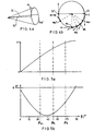
- Figure 4a shows one of the switching cones showing both of the possible fully switched positions DC and DC' of the director.
- the polarisation directors of the molecules, P s and P s ' respectively, are also shown. In practice, however, as will be discussed below, the director does not occupy these fully switched positions.
- Figure 4b shows a view of the cone from the end thereof (a so-called 'plan view') showing some positions of the director around the cone between position DC to position DC'.
- the director is assumed to rotate around the cone in a clockwise direction under the influence of an applied field of a certain polarity.
- the director of the liquid crystal molecules will only occupy the positions DC and DC' under the continued influence of an applied field of suitable polarity and sufficient magnitude. When such a field is not present the director relaxes around the cone away from the fully switched position to some extent.
- the director starts from an angle marked ⁇ ac because this is the position that the director will occupy in use as a result of a constant AC signal applied across the pixel.
- the AC field is continuously applied as a consequence of addressing the device as an array of pixels and will be explained further below.
- the angle ⁇ ac is a function of the distance of the director from the substrates of the device but here we use a uniform director model to assist explanation.
- the angles ⁇ ac and ⁇ ac ' will correspond to angles of ⁇ 22.5° in the plane of the device, in other words when the director is viewed normal to the device.
- the component of the AC stabilised director orientation in the plane of the device is 22.5° this results in the two AC stabilised positions of the director being perceived as 45° apart which gives the best brightness when crossed polarisers (at 90° to each other) are used with the device.
- the starting orientation is ⁇ ac and switching occurs when a net DC field of the correct polarity tends to cause reorientation towards ⁇ s (once the director has passed ⁇ s the pixel will have latched in the other state and the director will relax to the other side of the cone on removal of the DC field).
- Figure 5a shows the ferroelectric torque acting upon the director plotted against the director positions between DC and ⁇ s shown in figure 4.
- the ferroelectric torque is dependent upon the position of the director around the cone as shown in the graph and is also linearly related to the magnitude and direction of the applied field for a particular director orientation. This torque acts on the director to make it rotate around the switching cone.
- the dielectric, or electrostatic, torque, shown in figure 5b results from the ferroelectric material which aims to reduce the electrostatic free energy of the material, usually at a value of ⁇ ac close to 0° or 180°.
- the dielectric torque acts to oppose the ferroelectric torque, varies with the position of the director as shown in the graph and is also proportional to the square of the voltage of the applied field.
- the resultant torque ⁇ applied to the director can be calculated mathematically. This has been shown in "The effect of the biaxial permittivity tensor and tilted layer geometry on the switching of ferroelectric liquid crystals" by M. J. Towler, J. C. Jones and E. P Raynes published in 1992 Liquid Crystals Vol. 11 no. 3. An expression for the applied torque (ignoring elastic and inertial torques) is given by:
- ⁇ is the switching viscosity of the liquid crystal taken as 100 cP
- P s is the ferroelectric spontaneous polarisation taken as +5 nCcm -2
- ⁇ is the angle of director around the cone
- V is the applied voltage
- d is the spacing of the substrates of the device taken as 1.5 ⁇ m
- ⁇ is the permittivity of free space equal to 8.886x10 -12
- ⁇ is the smectic C cone angle (i.e. the angle between the director and the layer normal) taken as 22.5° ⁇ tilt angle of the layer normal from the substrate taken as 0.85 ⁇
- ⁇ is the uniaxial dielectric anisotropy taken as -1
- ⁇ is the dielectric biaxiality taken as +0.4
- Figure 6 shows a series of curves (for different applied voltages) of resultant torque against director orientation for a device having the parameter values noted above.
- the curve corresponding to 10 volt is the shallowest of the curves but corresponds to a positive switching torque ⁇ at all angles of the director between 50° and 90°. Positive values of ⁇ cause the director angle ⁇ to move towards 90° whereas negative values cause the director to move towards the AC field stabilised condition ⁇ ac .
- the higher voltage curves 20 volt to 60 volt, show that the application of a higher voltage results in a negative switching torque for small values of the switching angle ⁇ . This is the reason that there is a minimum value in the TV curve for certain ferroelectric liquid crystal materials. Above a certain applied voltage, the dielectric torque starts to dominate the switching torque and the pixel will not switch.
- Figure 9 and its associated description cover this in-more detail.
- the present invention is based upon the realisation that, for a ferroelectric LCD, the switching performance of the device can be improved by varying the voltage level of the switching pulse during the switching process.
- a switching voltage which gives maximum resultant torque r so the discrete example given above can be extended to drive the pixel with a voltage waveform that is substantially constantly varying.
- the optimum switching voltage can be derived by differentiating the torque equation, setting the result to zero and checking that the second differential is negative. This gives an equation for V as follows:
- Figure 7 shows three curves of voltage against director orientation for the case of maximum torque and the two cases of zero torque.
- the cases of zero torque are important for multiplex addressing of a FLCD.
- the difference between the switching and non-switching voltages should be as great as possible to give wide operating ranges of the device, in terms of temperature, voltage and structural non-uniformities.
- a prior art multiplex addressing scheme will now be described in order to explain switching and non-switching signals and discrimination between the two.
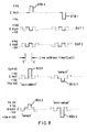
- Figure 8 shows a prior art monopulse addressing scheme for a ferroelectric liquid crystal array device in which a strobe signal is applied in succession to the row electrodes.
- the strobe signal comprises a positive going strobe pulse STB+ and a negative going strobe pulse STB-.
- the strobe pulses each having a period of zero volt followed by an equal period of magnitude Vs.
- Either of the two data pulses DAT1 and DAT2 having magnitudes of Vd may be applied to the column electrodes as required.
- a column driving arrangement must provide the appropriate data waveform to every column electrode.
- One of these data signal waveforms when combined with either STB+ or STB-, must cause the pixel to change state while the other data signal waveform combined with the strobe signal must not cause the pixel to change state.
- FIG 8 the combination of STB+ with DAT1 is shown at RES1 and this provides a NON-SELECT signal. It is important to remember that the voltages of the strobe signal and the data signals must be subtracted to give the resultant signal since they are applied to either side of a pixel.
- the combination of STB+ with DAT2 results in the signal shown at RES2 and this provides a SELECT signal.
- the pixel can either be left in the original state or switched to the state defined (in this example) by a positive-going pulse. The higher voltage signal thus provides non-switching of the pixel state.
- the JOERS/Alvey scheme described here is best applied to materials with ⁇ V minima and works as follows.
- the strobe voltage includes a zero voltage portion in the first part of the time slot and when this is combined with the data signals it provides a pre-pulse of ⁇ Vd followed by a time slot of voltage Vs ⁇ Vd.
- By operating the FLC device in a ⁇ V minimum mode gives a select resultant signal of (+Vd, Vs-Vd) and a non-select resultant signal of (-Vd, Vs+Vd).
- a strobe pulse STB- of the other polarity is required and this will provide a SELECT resultant signal RES3 with the data signal waveform DAT1 and a NON-SELECT resultant waveform RES4 with the data waveform DAT2.
- This scheme requires that two periods of strobe signal are provided for every row of the device to be addressed.
- An alternative technique provides a blanking pulse to every row in sequence at a time between 5 and 10 rows ahead of the strobe pulse.
- the blanking pulse has a large enough voltage-time product to switch all of the pixels in a row to one or other of the states regardless of whether the DAT 1 or the DAT2 signal waveform is being applied to each pixel (as a consequence of addressing another row of the device).
- only one strobe signal needs to be applied to the rows of the device since those pixels required to be dark (for example) are already dark and only those which need to be switched to the light state need to have a SELECT resultant signal applied to them.
- Figure 9 shows a graph of switching time T against applied voltage V for a typical passive ferroelectric liquid crystal device.
- the lower pair of curves S (solid and broken lines) relate to the switching resultant signal applied to a pixel and the upper pair of curves NS relate to the non-switching resultant signal.
- the lower solid curve (100%) gives the minimum time and voltage product required to switch all of the directors within a pixel into the other state.
- the broken line (0%) beneath it gives the time and voltage product at which the directors in a pixel will just start to switch. As the voltage is increased and the time reduced, however, the non-switching curve becomes significant.
- This curve gives the minimum time and voltage product for the directors in a pixel not to switch to the other state and is related to the upper curve in figure 7.
- the upper curve shown in broken lines is analogous to that for the switching curve.
- the inverted operating region of the device lies the inverted operating region of the device.
- This area is shaded in coarse hatching in the figure and the larger this region is, the greater the discrimination between switching and non-switching of the device in this operational mode.
- the switching resultant signal must lie within the operating region and the non-switching resultant signal must lie outside this region. Therefore, the combination of the strobe signal and the non-switching data signal must result in a ⁇ V product that falls outside of the operating region. Conversely, the combination of the strobe signal and the switching data signal must result in a ⁇ V product that falls within the FS region.
- a large margin of discrimination is particularly important because the ferroelectric LCD is particularly sensitive to temperature and as the device heats up, the position of the TV switching curves move.
- the area of inverted operation of the figure discussed thus far is suitable for driving by the JOERS/Alvey driving scheme of GB 2,146,743.
- the other hatched area in the figure show a so-called conventional mode of operation in which the switching and non-switching resultant signals for driving the device are reversed.
- the driving waveforms described herein are applicable to operation in this region by reversing the switching and non-switching resultant signals.
- the strobe signal may be arranged to be a square wave signal and the data signals can be varying, the strobe signal may be arranged to be varying and the data signals may be square wave signals or both the data signals and the strobe signal may be continuously varying.
- the present inventors have used a numerical integration of the torque equation to derive switching voltages as a function of time from the torque versus director orientation expressions.
- the version of the torque equation used does include an empirical elastic term as given by Towler in Proceeding 163 published together with the previous identified conference reference at pages 403 to 404. This allows the optimum resultant signal to be computed although practical constraints, as will be seen, place some restrictions on the signals actually applied to devices in accordance with the invention.
- the results of one set of approximations (using the parameters previously described) is shown in figure 10.
- the curve A represents the voltage to be applied to a pixel for the fastest possible switching.
- Figure 11 shows a graph of director orientation against time derived from the numerical integration calculation.
- Figure 12 shows strobe, data and resultant signals based on the curves of figures 10 and 11.
- Figure 12 (a) shows a strobe signal S
- figure 12 (b) shows a white data signal Vw
- ad figure 12 (c) shows the resultant signal for switching S-Vw.
- the data signal is referred to as a white data signal since the display device is assumed to be blanked to black before the application of the strobe signal to a particular row.
- the switching data signal is a white data signal and the non-switching data signal is a black data signal.
- the resultant switching signal corresponds with that shown in figure 11 for the voltage signal resulting in fastest switching of the pixel state.
- the display device can be blanked to white and switched to black.
- Figure 13 shows strobe, data and resultant signals for a non-switching or black data signal.
- Figure 13 (a) shows a strobe signal identical to that of figure 12 (a) as it must be for a practical device.
- the black data signal is shown at figure 13 (b) and is the inverse of the white data signal. Although not essential this is a very effective way of complying with design restrictions placed on these signal waveforms as will be discussed below.
- Figure 13 (c) shows the resultant signal of the strobe and the black data signal. By referring to figure 9 it can be appreciated that this signal waveform is of too low a voltage and too short a duration to cause the pixel to change state.
- the white data and black data waveforms should have equivalent RMS voltages which imposes the constraint:
- One of the simplest conceivable combinations of strobe and data signals to provide the optimum resultant signal would be to provide a strobe signal equal to half the optimum resultant signal and a non-select data signal identical to the strobe signal and a select data signal equal to the inverse of the non-select data signal. This would provide both the optimum switching waveform and a non-select resultant signal having an optimum value of zero.
- this combination of signals does not meet the constraint that the data signals should be DC balanced.
- the non-select resultant signal may be chosen to comprise portions of the high voltage non-select voltage (curve B in figure 10) and even arranging for the voltage to be negative to switch the director in the wrong direction (for example curve C in figure 10).
- the curves shown in figures 12 and 13 provide both the optimum switching resultant signal and a non-switching resultant signal that provides a high level of discrimination between the select and non-select resultant signals. Means for applying these desired signal waveforms to a FLCD will be described subsequently.
- the driving technique of the present invention uses signals of both positive and negative polarity. For this, the definition of zero volt can be taken as that on a shortcircuited element of the device after it has reached equilibrium ("infinite time").
- Figure 14 shows strobe, data and resultant signals derived from those shown in figures 12 and 13.
- a voltage limit is applied to both the strobe and the data signals in order to provide a realisable resultant signal.
- the strobe signal shown at figure 14 (i) has been limited to a maximum value of 60 volt and the data signals shown at figures 14 (a)(ii) and 14 (b)(ii) have been limited to a maximum value of 50 volt.
- the select resultant signal shown at figure 14 (b)(iii) is slightly longer than the select resultant signal shown in figure 12 and includes a short section at the end of the line address time at the maximum value of 110 volt.
- the extra time required to cause the pixels to change state, however, is very short.
- the total time to switch the pixels using the signal shown in figure 14 (b)(iii) is 14 ⁇ s which is only very slightly longer than the theoretical minimum value of 13.4 ⁇ s.
- the data signals may be subject to lower maximum voltage constraints.
- the reason that such a limitation in data voltage may be desirable is a consequence of device heating considerations.
- a large area FLCD presents a load to the driving circuitry that comprises a large number of long RC ladders.
- the data signals are applied to the device continuously and, since the electrode tracks tend to exhibit quite a high resistance, significant heating of the ferroelectric liquid crystal device can occur.
- high values of RMS data voltage can cause significant heating of the device.
- the magnitude and/or shape of the strobe and/or data signals may be varied to compensate.
- a switching technique that provides a square wave style strobe signal in combination with a continuously varying data signal.
- This has the advantage over the previous described embodiment that continuously varying voltage driver circuitry needs only to be supplied for the column drivers of the FLCD providing savings of complexity and cost.
- Figure 15 shows a driving scheme for a passive ferroelectric liquid crystal device which provides only a positive-going strobe signal for use in conjunction with a blanking pulse (not shown) as discussed above with reference to figure 9.
- Figure 16 shows a scheme in which both a positive-going strobe signal and a negative-going strobe signal are provided.
- a strobe signal STB has a portion of zero volt followed by a rather longer portion of +V s volt.
- Data signals DATa and DATb are shown on the line beneath identical representations of the strobe signal STB. Both DATa and DATb are DC balanced as discussed above.
- the resultant of the signal DATa when combined with the strobe signal STB is shown as RESa which provides a smoothly increasing voltage across the liquid crystal pixel.
- This provides a SELECT resultant signal which causes the pixel to change state.
- the resultant of the signal DATb when combined with the strobe signal STB is shown as RESb which provides a signal shown at RESb.
- the signal RESb comprises a pre-pulse (during the period at which STB is zero volt) which actually drives the directors in the pixel away from the switching direction as described previously to help ensure that undesired switching of the directors does not take place.
- the signal RESb then continues to a positive-going peak and smoothly reduces until the end of the strobe signal STB. This provides a non-select resultant signal which leaves the pixel in its original state.
- Figure 16 shows a pair of strobe signals STB+ and STB- which each comprise a section of zero volt followed by a section of magnitude V s .
- a first data signal DATc is shown beneath both of the strobe signals and on the next line and a second data signal DATd is shown beneath both of the strobe signal on the line below that.
- the combination of STB+ and DATc gives RESc which comprises a small negative-going pre-pulse followed by a positive-going pulse that peaks and then steadily reduces in voltage until the end of the strobe pulse.
- the combination of STB+ with signal DATd gives a resultant as shown at RESd with a profile that increases swiftly at first followed by a more gentle increase until the end of the strobe signal.
- the combination of STB- with DATc provides a resultant signal shown as RESe which is the inverse of RESd.
- the combination of STB- with DATd provides a resultant signal shown as RESf which is the inverse of the signal RESc.
- FIG 17 shows a block schematic diagram of a driving arrangement 100 in accordance with the present invention.
- a liquid crystal array 102 comprises a plurality of columns numbered 1 to n of which numbers 1, 2, 3 and n are shown.
- the driving of the array is controlled by a clock generator 104 which governs the timing of the signals applied to the array.
- the clock generator 104 is connected to a row driver 106 which is connected to all of the rows of the array to provide the strobe signals at the correct time to the appropriate row.
- the clock generator is also connected to a data source 108 which provides the data relating to the desired state of each pixel in a particular row for each application of the strobe signal.
- a signal from the clock generator 104 clocks this data into a shift register 110 every time that a new row is addressed.
- the shift register has n outputs Q1 to Qn, in other words one for each column of the display, and each of these outputs controls one of n analogue switches 112. Under the control of the outputs of the shift register 110, the analogue switches couple either a SELECT or a NON-SELECT data signal to their respective columns of the array.
- the SELECT data signal is provided by a digital to analogue converter (DAC) 120 which is provided with digital data from a random access memory (RAM) 116.
- the NON-SELECT data signal is provided by a DAC 118 provided with digital data from a RAM 114.
- the RAM 116 and the RAM 118 contain digitised versions of the SELECT data and NON-SELECT data signals shown, for example, in figure 11.
- the RAMs are addressed by the clock generator 104 providing a parallel signal which counts up at a fast rate to clock the digital signals representing the data signals out of the RAMs.
- the DACs convert these signals into a pair of substantially continuously varying signals which are applied to respective poles of the switches 112.
- the relevant data signal is selected from the outputs of the DACs by the plurality of switches 112 and the required combination of strobe signal and data signal waveform can be applied to each pixel in the array.
- the RAMs must be clocked at a sufficiently high rate and the RAM/DAC combination must be of high enough resolution to mimic the desired switching signal waveform accurately.
- the row driver may be arranged to provide a bi-directional strobe signal of the type shown in figure 16 or a blanking pulse ahead of the application of the strobe signal.
- the blanking pulse is chosen to switch the pixels in a particular row into a given state regardless of the data waveform applied to the pixel at that instant.
- the blanking pulse may be arranged to comprise a signal having at least a portion of which is a continuously varying signal.
- the RAM 114 and the DAC 118 can be omitted.
- the NON-SELECT waveform may be derived from the SELECT waveform by using an inverting buffer connected to the output of the DAC 120.
- the shift register may be omitted and the data source connected to control the analogue switches 112 directly.
- the clock generator 104 may also be provided with means to alter the data signals in response to operational data from the liquid crystal device array. For example, it may be desired to change the amplitude and/or the shape of the data waveforms as the array becomes hotter in use.
- Temperature measurement techniques are known for large area array devices to provide temperature variation details. Temperature compensation can then be readily achieved by providing the data corresponding to the further signals in the RAM and altering the addressing of the RAM to output the modified data signals as appropriate. Further details are available, inter alia, from: International Patent Application Publication number WO95/24715, United Kingdom Patent Publication number GB2207272 and United States Patent US 4923285.
- a further memory and digital to analogue converter are provided in place of the row driver 106.
- the memory for example a further RAM
- the digital to analogue converter would convert this data into a continuously varying signal and conventional row driving means could be used to apply the strobe signal to the rows of the array in the correct sequence.
- Means for providing a blanking pulse may be provided in accordance with known techniques or a further memory and digital to analogue converter may be provided to provide a complementary strobe signal. Where the complementary strobe signal is an inverted version of the other strobe signal, a saving may be effected as described above with reference to the data signals.
- the present invention may be used to apply a continuously varying strobe signal in conjunction with square wave style data signals. This would provide a compromise similar to that described with reference to figures 15 and 16. A possible scheme is shown in figure 18.
- Figure 18 (i) shows a continuously varying strobe signal in accordance with the invention.
- Figure 18 (ii) (a) shows a two-slot non-select data signal as is known from the prior art scheme described with reference to figure 8.
- Figure 18 (ii) (b) shows a two-slot select data signal which is the inverse of that shown in figure 18 (i) (a).
- Figure 18 (iii) shows the resultant signal where (a) is the non-select resultant and (b) is the select resultant.
- the non-select resultant has a negative-going pre-pulse followed by a high voltage pulse which does not switch the pixel.
- the select resultant pulse provides a smoothly increasing switching pulse providing a good approximation to that shown in figure 10.
- Figure 19 shows a further example of data, strobe and resultant signals which is a variation on those shown in figure 18.
- Figure 19 (i) shows a continuously varying strobe signal in accordance with the invention.
- Figure 19 (ii) (a) shows a two-slot non-select data signal as is known from the prior art scheme described with reference to figure 8.
- Figure 19 (ii) (b) shows a two-slot select data signal which is the inverse of that shown in figure 19 (i) (a).
- Figure 19 (iii) shows the resultant signal where (a) is the non-select resultant and (b) is the select resultant.
- The. non-select resultant has a negative-going pre-pulse followed by a high voltage pulse which does not switch the pixel.
- the select resultant pulse provides a smoothly increasing switching pulse providing a good approximation to that shown in figure 10.
- Figure 20 shows strobe, data and resultant signals in accordance with the invention in which the select (figure 20 (b)(ii)) and the non-select (figure 20 (a)(ii)) data signals differ from one another in shape. These data signals still fulfil the requirements set out previously for the data signals.
- Figure 20 (a)(iii) shows the non-select resultant which comprises a high voltage level initially to exploit the curve B characteristics of a device described with respect to figure 10. As the resultant voltage for non-select performance increases, the resultant signal is arranged to have a voltage close to zero to continue to ensure that no significant switching torque is applied to the directors of a device.
- the switching resultant curve shown in figure 20 (b)(iii) is a close approximation to the ideal switching torque curve A shown in figure 10.
- the strobe signal waveform may be arranged to extend into the 1.a.t. of the following row as disclosed in UK Patent number 2,262,831.
- the examples have concentrated on a passive FLCD device but the invention is applicable to any passive liquid crystal device in which the response depends upon the polarity of the applied signal.
- passive liquid crystal devices include electroclinic liquid crystal devices (for example in the smectic A* phase), those exploiting flexoelectric effects and some nematic liquid crystal devices.
Landscapes
- Engineering & Computer Science (AREA)
- Chemical & Material Sciences (AREA)
- Crystallography & Structural Chemistry (AREA)
- Physics & Mathematics (AREA)
- Computer Hardware Design (AREA)
- General Physics & Mathematics (AREA)
- Theoretical Computer Science (AREA)
- Liquid Crystal Display Device Control (AREA)
- Liquid Crystal (AREA)
Applications Claiming Priority (2)
| Application Number | Priority Date | Filing Date | Title |
|---|---|---|---|
| GB9610312 | 1996-05-17 | ||
| GB9610312A GB2313223A (en) | 1996-05-17 | 1996-05-17 | Liquid crystal device |
Publications (2)
| Publication Number | Publication Date |
|---|---|
| EP0809232A2 true EP0809232A2 (fr) | 1997-11-26 |
| EP0809232A3 EP0809232A3 (fr) | 1997-12-03 |
Family
ID=10793846
Family Applications (1)
| Application Number | Title | Priority Date | Filing Date |
|---|---|---|---|
| EP97303366A Withdrawn EP0809232A3 (fr) | 1996-05-17 | 1997-05-16 | Circuit et méthode de commande pour dispositif à cristaux liquides |
Country Status (4)
| Country | Link |
|---|---|
| US (1) | US6057821A (fr) |
| EP (1) | EP0809232A3 (fr) |
| JP (1) | JPH1054972A (fr) |
| GB (1) | GB2313223A (fr) |
Families Citing this family (8)
| Publication number | Priority date | Publication date | Assignee | Title |
|---|---|---|---|---|
| US6897855B1 (en) * | 1998-02-17 | 2005-05-24 | Sarnoff Corporation | Tiled electronic display structure |
| US6466189B1 (en) * | 2000-03-29 | 2002-10-15 | Koninklijke Philips Electronics N.V. | Digitally controlled current integrator for reflective liquid crystal displays |
| US6496173B1 (en) * | 2000-03-29 | 2002-12-17 | Koninklijke Philips Electronics N.V. | RLCD transconductance sample and hold column buffer |
| DE60307101T2 (de) * | 2002-05-29 | 2007-01-04 | Zbd Displays Ltd., Malvern | Anzeigevorrichtung mit einem material mit mindestens zwei stabilen zuständen und ansteuerverfahren dafür |
| US7557789B2 (en) * | 2005-05-09 | 2009-07-07 | Texas Instruments Incorporated | Data-dependent, logic-level drive scheme for driving LCD panels |
| US8384639B2 (en) * | 2006-02-07 | 2013-02-26 | Sharp Kabushiki Kaisha | Liquid crystal display device and method for emphasizing temporal signal change on a video signal based on at least a polarity for the video signal |
| US7782438B2 (en) * | 2006-06-13 | 2010-08-24 | Kent State University | Fast switching electro-optical devices using banana-shaped liquid crystals |
| GB0903383D0 (en) * | 2009-02-27 | 2009-04-08 | Syngenta Ltd | Sensor |
Family Cites Families (16)
| Publication number | Priority date | Publication date | Assignee | Title |
|---|---|---|---|---|
| GB2064194B (en) * | 1978-02-08 | 1982-08-04 | Sharp Kk | Matrix type liquid crystal display device |
| GB2077974B (en) * | 1978-10-25 | 1983-01-06 | Sharp Kk | A matrix type liquid crystal display device |
| US5227905A (en) * | 1980-01-08 | 1993-07-13 | Clark Noel A | Surface stabilized ferroelectric liquid crystal devices |
| GB2118346B (en) * | 1982-04-01 | 1985-07-24 | Standard Telephones Cables Ltd | Scanning liquid crystal display cells |
| JPS61163324A (ja) * | 1985-01-14 | 1986-07-24 | Canon Inc | 液晶セルの駆動方法 |
| DE3686462T2 (de) * | 1985-09-06 | 1993-01-21 | Matsushita Electric Ind Co Ltd | Verfahren zur ansteuerung eines fluessigkristallrasterbildschirmes. |
| DE3784809T2 (de) * | 1986-08-18 | 1993-07-08 | Canon Kk | Verfahren und vorrichtung zur ansteuerung einer optischen modulationsanordnung. |
| NL8703040A (nl) * | 1987-12-16 | 1989-07-17 | Philips Nv | Werkwijze voor het besturen van een passieve ferro-elektrisch vloeibaar kristal weergeefinrichting. |
| GB8808812D0 (en) * | 1988-04-14 | 1988-05-18 | Emi Plc Thorn | Display device |
| NL8901184A (nl) * | 1989-05-11 | 1990-12-03 | Philips Nv | Passieve weergeefinrichting. |
| JP2682886B2 (ja) * | 1990-04-25 | 1997-11-26 | シャープ株式会社 | 表示装置の駆動方法 |
| IT1240381B (it) * | 1990-07-06 | 1993-12-10 | Seleco Spa | Circuito generatore di segnali di pilotaggio per display |
| US5170271A (en) * | 1991-01-31 | 1992-12-08 | Hughes Aircraft Company | Shaped voltage pulse method for operating a polymer dispersed liquid crystal cell, and light valve employing the same |
| DE69317640T2 (de) * | 1992-12-28 | 1998-07-30 | Canon Kk | Verfahren und Einrichtung für eine Flüssigkristallanzeige |
| BE1007478A3 (nl) * | 1993-09-07 | 1995-07-11 | Philips Electronics Nv | Weergeefinrichting met temperatuurcompensatie. |
| US5731797A (en) * | 1994-10-06 | 1998-03-24 | Matsushita Electric Industrial Co., Ltd. | Driving method for spatial light modulator and projection display system |
-
1996
- 1996-05-17 GB GB9610312A patent/GB2313223A/en not_active Withdrawn
-
1997
- 1997-05-15 US US08/856,720 patent/US6057821A/en not_active Expired - Fee Related
- 1997-05-16 JP JP9127704A patent/JPH1054972A/ja active Pending
- 1997-05-16 EP EP97303366A patent/EP0809232A3/fr not_active Withdrawn
Also Published As
| Publication number | Publication date |
|---|---|
| EP0809232A3 (fr) | 1997-12-03 |
| GB9610312D0 (en) | 1996-07-24 |
| GB2313223A (en) | 1997-11-19 |
| US6057821A (en) | 2000-05-02 |
| JPH1054972A (ja) | 1998-02-24 |
Similar Documents
| Publication | Publication Date | Title |
|---|---|---|
| KR0136798B1 (ko) | 액정셀의 어드레싱 방법 및 이를 이용한 장치 | |
| EP0177365A2 (fr) | Dispositif d'affichage à cristal liquide pour multiplexage à division du temps | |
| US8013819B2 (en) | Drive scheme for a cholesteric liquid crystal display device | |
| EP0224243A2 (fr) | Dispositif de modulation optique et procédé de commande de celui-ci | |
| EP0564263B1 (fr) | Dispositif d'affichage | |
| US6351256B1 (en) | Addressing method and apparatus | |
| US6057821A (en) | Liquid crystal device | |
| US7173587B2 (en) | Addressing process and device for a bistable liquid crystal screen | |
| CN1256761A (zh) | 反铁电液晶显示器及其驱动方法 | |
| KR19990008127A (ko) | 액정 디스플레이 장치 | |
| KR100444006B1 (ko) | 강유전체액정디스플레이및멀티플렉스어드레싱방법 | |
| Maltese | Advances and problems in the development of ferroelectric liquid crystal displays | |
| KR100324438B1 (ko) | 액정 디바이스 및 액정 디바이스의 어드레스 방법 | |
| US6046715A (en) | Liquid crystal array device | |
| KR100279684B1 (ko) | 액정 디바이스 및 액정 디바이스를 어드레싱하는 방법 | |
| US20070013860A1 (en) | Bistable liquid crystal display device including improved addressing means | |
| EP0838802A2 (fr) | Méthode et dispositif d'adressage d'un dispositif d'affichage à cristaux liquides ferroélectriques et dispositif d'affichage à cristaux liquides ferroélectriques | |
| GB2347258A (en) | Matrix array bistable devices | |
| GB2293908A (en) | Liquid crystal display element | |
| JP2000035563A (ja) | 強誘電性液晶デバイス | |
| JPS63249130A (ja) | 液晶装置の駆動法 | |
| Ross | Ferroelectric liquid crystal displays | |
| GB2293905A (en) | Addressing a liquid crystal display | |
| JPH0579968B2 (fr) | ||
| JPH09236829A (ja) | 反強誘電性液晶表示素子およびその駆動方法 |
Legal Events
| Date | Code | Title | Description |
|---|---|---|---|
| PUAI | Public reference made under article 153(3) epc to a published international application that has entered the european phase |
Free format text: ORIGINAL CODE: 0009012 |
|
| PUAL | Search report despatched |
Free format text: ORIGINAL CODE: 0009013 |
|
| AK | Designated contracting states |
Kind code of ref document: A2 Designated state(s): DE FR GB NL |
|
| AK | Designated contracting states |
Kind code of ref document: A3 Designated state(s): DE FR GB NL |
|
| 17P | Request for examination filed |
Effective date: 19980601 |
|
| 17Q | First examination report despatched |
Effective date: 20020529 |
|
| STAA | Information on the status of an ep patent application or granted ep patent |
Free format text: STATUS: THE APPLICATION IS DEEMED TO BE WITHDRAWN |
|
| 18D | Application deemed to be withdrawn |
Effective date: 20031027 |