US7166908B2 - Optical device - Google Patents
Optical device Download PDFInfo
- Publication number
- US7166908B2 US7166908B2 US11/244,083 US24408305A US7166908B2 US 7166908 B2 US7166908 B2 US 7166908B2 US 24408305 A US24408305 A US 24408305A US 7166908 B2 US7166908 B2 US 7166908B2
- Authority
- US
- United States
- Prior art keywords
- optical
- optical element
- device substrate
- opening mouth
- terminal portions
- Prior art date
- Legal status (The legal status is an assumption and is not a legal conclusion. Google has not performed a legal analysis and makes no representation as to the accuracy of the status listed.)
- Expired - Fee Related
Links
- 230000003287 optical effect Effects 0.000 title claims abstract description 382
- 239000000758 substrate Substances 0.000 claims abstract description 144
- 239000008393 encapsulating agent Substances 0.000 claims description 6
- 238000012360 testing method Methods 0.000 description 91
- 238000000034 method Methods 0.000 description 63
- 235000012431 wafers Nutrition 0.000 description 48
- 238000000465 moulding Methods 0.000 description 36
- 239000003550 marker Substances 0.000 description 28
- 239000000047 product Substances 0.000 description 20
- 238000007789 sealing Methods 0.000 description 15
- 230000000007 visual effect Effects 0.000 description 14
- 230000002950 deficient Effects 0.000 description 12
- 238000004519 manufacturing process Methods 0.000 description 9
- 239000011347 resin Substances 0.000 description 9
- 229920005989 resin Polymers 0.000 description 9
- 230000015572 biosynthetic process Effects 0.000 description 7
- 239000012467 final product Substances 0.000 description 7
- 238000004458 analytical method Methods 0.000 description 6
- 238000003384 imaging method Methods 0.000 description 6
- 230000000694 effects Effects 0.000 description 5
- 238000012545 processing Methods 0.000 description 5
- 239000007787 solid Substances 0.000 description 5
- 230000002093 peripheral effect Effects 0.000 description 4
- 239000000088 plastic resin Substances 0.000 description 4
- 239000011800 void material Substances 0.000 description 4
- ATJFFYVFTNAWJD-UHFFFAOYSA-N Tin Chemical compound [Sn] ATJFFYVFTNAWJD-UHFFFAOYSA-N 0.000 description 3
- 238000002834 transmittance Methods 0.000 description 3
- 235000016496 Panda oleosa Nutrition 0.000 description 2
- 240000000220 Panda oleosa Species 0.000 description 2
- 239000003822 epoxy resin Substances 0.000 description 2
- 238000005530 etching Methods 0.000 description 2
- 239000011521 glass Substances 0.000 description 2
- 229920000647 polyepoxide Polymers 0.000 description 2
- 239000000919 ceramic Substances 0.000 description 1
- 230000007547 defect Effects 0.000 description 1
- 238000013095 identification testing Methods 0.000 description 1
- 230000009545 invasion Effects 0.000 description 1
- 239000000463 material Substances 0.000 description 1
- 238000005259 measurement Methods 0.000 description 1
- 239000000203 mixture Substances 0.000 description 1
- 238000004806 packaging method and process Methods 0.000 description 1
- 238000011056 performance test Methods 0.000 description 1
- 230000001105 regulatory effect Effects 0.000 description 1
- 239000004065 semiconductor Substances 0.000 description 1
Images


Classifications
-
- H—ELECTRICITY
- H01—ELECTRIC ELEMENTS
- H01L—SEMICONDUCTOR DEVICES NOT COVERED BY CLASS H10
- H01L27/00—Devices consisting of a plurality of semiconductor or other solid-state components formed in or on a common substrate
- H01L27/14—Devices consisting of a plurality of semiconductor or other solid-state components formed in or on a common substrate including semiconductor components sensitive to infrared radiation, light, electromagnetic radiation of shorter wavelength or corpuscular radiation and specially adapted either for the conversion of the energy of such radiation into electrical energy or for the control of electrical energy by such radiation
-
- H—ELECTRICITY
- H01—ELECTRIC ELEMENTS
- H01L—SEMICONDUCTOR DEVICES NOT COVERED BY CLASS H10
- H01L31/00—Semiconductor devices sensitive to infrared radiation, light, electromagnetic radiation of shorter wavelength or corpuscular radiation and specially adapted either for the conversion of the energy of such radiation into electrical energy or for the control of electrical energy by such radiation; Processes or apparatus specially adapted for the manufacture or treatment thereof or of parts thereof; Details thereof
- H01L31/02—Details
- H01L31/0203—Containers; Encapsulations, e.g. encapsulation of photodiodes
-
- H—ELECTRICITY
- H01—ELECTRIC ELEMENTS
- H01L—SEMICONDUCTOR DEVICES NOT COVERED BY CLASS H10
- H01L23/00—Details of semiconductor or other solid state devices
- H01L23/02—Containers; Seals
-
- H—ELECTRICITY
- H01—ELECTRIC ELEMENTS
- H01L—SEMICONDUCTOR DEVICES NOT COVERED BY CLASS H10
- H01L27/00—Devices consisting of a plurality of semiconductor or other solid-state components formed in or on a common substrate
- H01L27/14—Devices consisting of a plurality of semiconductor or other solid-state components formed in or on a common substrate including semiconductor components sensitive to infrared radiation, light, electromagnetic radiation of shorter wavelength or corpuscular radiation and specially adapted either for the conversion of the energy of such radiation into electrical energy or for the control of electrical energy by such radiation
- H01L27/144—Devices controlled by radiation
- H01L27/146—Imager structures
- H01L27/14601—Structural or functional details thereof
- H01L27/14618—Containers
-
- H—ELECTRICITY
- H01—ELECTRIC ELEMENTS
- H01L—SEMICONDUCTOR DEVICES NOT COVERED BY CLASS H10
- H01L27/00—Devices consisting of a plurality of semiconductor or other solid-state components formed in or on a common substrate
- H01L27/14—Devices consisting of a plurality of semiconductor or other solid-state components formed in or on a common substrate including semiconductor components sensitive to infrared radiation, light, electromagnetic radiation of shorter wavelength or corpuscular radiation and specially adapted either for the conversion of the energy of such radiation into electrical energy or for the control of electrical energy by such radiation
- H01L27/144—Devices controlled by radiation
- H01L27/146—Imager structures
- H01L27/14683—Processes or apparatus peculiar to the manufacture or treatment of these devices or parts thereof
-
- H—ELECTRICITY
- H01—ELECTRIC ELEMENTS
- H01L—SEMICONDUCTOR DEVICES NOT COVERED BY CLASS H10
- H01L31/00—Semiconductor devices sensitive to infrared radiation, light, electromagnetic radiation of shorter wavelength or corpuscular radiation and specially adapted either for the conversion of the energy of such radiation into electrical energy or for the control of electrical energy by such radiation; Processes or apparatus specially adapted for the manufacture or treatment thereof or of parts thereof; Details thereof
- H01L31/18—Processes or apparatus specially adapted for the manufacture or treatment of these devices or of parts thereof
-
- H—ELECTRICITY
- H01—ELECTRIC ELEMENTS
- H01L—SEMICONDUCTOR DEVICES NOT COVERED BY CLASS H10
- H01L2224/00—Indexing scheme for arrangements for connecting or disconnecting semiconductor or solid-state bodies and methods related thereto as covered by H01L24/00
- H01L2224/01—Means for bonding being attached to, or being formed on, the surface to be connected, e.g. chip-to-package, die-attach, "first-level" interconnects; Manufacturing methods related thereto
- H01L2224/02—Bonding areas; Manufacturing methods related thereto
- H01L2224/04—Structure, shape, material or disposition of the bonding areas prior to the connecting process
- H01L2224/05—Structure, shape, material or disposition of the bonding areas prior to the connecting process of an individual bonding area
- H01L2224/0554—External layer
- H01L2224/0556—Disposition
- H01L2224/05568—Disposition the whole external layer protruding from the surface
-
- H—ELECTRICITY
- H01—ELECTRIC ELEMENTS
- H01L—SEMICONDUCTOR DEVICES NOT COVERED BY CLASS H10
- H01L2224/00—Indexing scheme for arrangements for connecting or disconnecting semiconductor or solid-state bodies and methods related thereto as covered by H01L24/00
- H01L2224/01—Means for bonding being attached to, or being formed on, the surface to be connected, e.g. chip-to-package, die-attach, "first-level" interconnects; Manufacturing methods related thereto
- H01L2224/02—Bonding areas; Manufacturing methods related thereto
- H01L2224/04—Structure, shape, material or disposition of the bonding areas prior to the connecting process
- H01L2224/05—Structure, shape, material or disposition of the bonding areas prior to the connecting process of an individual bonding area
- H01L2224/0554—External layer
- H01L2224/05573—Single external layer
-
- H—ELECTRICITY
- H01—ELECTRIC ELEMENTS
- H01L—SEMICONDUCTOR DEVICES NOT COVERED BY CLASS H10
- H01L2224/00—Indexing scheme for arrangements for connecting or disconnecting semiconductor or solid-state bodies and methods related thereto as covered by H01L24/00
- H01L2224/01—Means for bonding being attached to, or being formed on, the surface to be connected, e.g. chip-to-package, die-attach, "first-level" interconnects; Manufacturing methods related thereto
- H01L2224/10—Bump connectors; Manufacturing methods related thereto
- H01L2224/15—Structure, shape, material or disposition of the bump connectors after the connecting process
- H01L2224/16—Structure, shape, material or disposition of the bump connectors after the connecting process of an individual bump connector
-
- H—ELECTRICITY
- H01—ELECTRIC ELEMENTS
- H01L—SEMICONDUCTOR DEVICES NOT COVERED BY CLASS H10
- H01L2924/00—Indexing scheme for arrangements or methods for connecting or disconnecting semiconductor or solid-state bodies as covered by H01L24/00
- H01L2924/0001—Technical content checked by a classifier
- H01L2924/00014—Technical content checked by a classifier the subject-matter covered by the group, the symbol of which is combined with the symbol of this group, being disclosed without further technical details
-
- H—ELECTRICITY
- H01—ELECTRIC ELEMENTS
- H01L—SEMICONDUCTOR DEVICES NOT COVERED BY CLASS H10
- H01L2924/00—Indexing scheme for arrangements or methods for connecting or disconnecting semiconductor or solid-state bodies as covered by H01L24/00
- H01L2924/15—Details of package parts other than the semiconductor or other solid state devices to be connected
- H01L2924/151—Die mounting substrate
- H01L2924/153—Connection portion
- H01L2924/1531—Connection portion the connection portion being formed only on the surface of the substrate opposite to the die mounting surface
- H01L2924/15311—Connection portion the connection portion being formed only on the surface of the substrate opposite to the die mounting surface being a ball array, e.g. BGA
-
- H—ELECTRICITY
- H01—ELECTRIC ELEMENTS
- H01L—SEMICONDUCTOR DEVICES NOT COVERED BY CLASS H10
- H01L2924/00—Indexing scheme for arrangements or methods for connecting or disconnecting semiconductor or solid-state bodies as covered by H01L24/00
- H01L2924/15—Details of package parts other than the semiconductor or other solid state devices to be connected
- H01L2924/151—Die mounting substrate
- H01L2924/153—Connection portion
- H01L2924/1532—Connection portion the connection portion being formed on the die mounting surface of the substrate
-
- H—ELECTRICITY
- H01—ELECTRIC ELEMENTS
- H01L—SEMICONDUCTOR DEVICES NOT COVERED BY CLASS H10
- H01L2924/00—Indexing scheme for arrangements or methods for connecting or disconnecting semiconductor or solid-state bodies as covered by H01L24/00
- H01L2924/15—Details of package parts other than the semiconductor or other solid state devices to be connected
- H01L2924/161—Cap
- H01L2924/1615—Shape
- H01L2924/16195—Flat cap [not enclosing an internal cavity]
-
- H—ELECTRICITY
- H01—ELECTRIC ELEMENTS
- H01L—SEMICONDUCTOR DEVICES NOT COVERED BY CLASS H10
- H01L33/00—Semiconductor devices having potential barriers specially adapted for light emission; Processes or apparatus specially adapted for the manufacture or treatment thereof or of parts thereof; Details thereof
- H01L33/48—Semiconductor devices having potential barriers specially adapted for light emission; Processes or apparatus specially adapted for the manufacture or treatment thereof or of parts thereof; Details thereof characterised by the semiconductor body packages
- H01L33/483—Containers
- H01L33/486—Containers adapted for surface mounting
-
- H—ELECTRICITY
- H01—ELECTRIC ELEMENTS
- H01L—SEMICONDUCTOR DEVICES NOT COVERED BY CLASS H10
- H01L33/00—Semiconductor devices having potential barriers specially adapted for light emission; Processes or apparatus specially adapted for the manufacture or treatment thereof or of parts thereof; Details thereof
- H01L33/48—Semiconductor devices having potential barriers specially adapted for light emission; Processes or apparatus specially adapted for the manufacture or treatment thereof or of parts thereof; Details thereof characterised by the semiconductor body packages
- H01L33/58—Optical field-shaping elements
Definitions
- the present invention relates to optical devices and more particularly relates to an optical device including an optical element chip in which an optical device for emitting and receiving light.
- optical semiconductor devices such as CCD modules included in a video camera, a digital camera, a digital still camera and the like have been known.
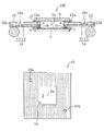
- a CCD package module 90 packaged by a flip-chip bonding technique are disclosed.
- a direct circuit (device substrate) 94 is provided mainly on a bottom surface of a glass (translucent member) 92 , and the direct circuit 94 is bonded to an image capture chip (optical element chip) 91 by flip-chip packaging bonding.
- the direct circuit 94 is bonded to a printing circuit board (wiring board) 96 via a tin ball 93 by circuit binding.
- a circuit is formed and packaged using the flip-chip bonding technique or various different substrates are combined to one another by the flip-chip bonding technique to form a package module for a thin type CCD image capture chip.
- the thickness of a package module for an image capture chip of a charge coupled device can be reduced.
- light subjected to image processing by the CCD package module 90 passes through an imaging loci p and is received by an image capture chip 91 .
- the CCD package module 90 With the image capture chip 91 mounted on the printing circuit board 96 , a voltage is applied to the image capture chip 91 , thereby performing image processing. Therefore, it is necessary to mount the image capture chip 91 on the printing circuit board 96 so that the image capture chip 91 is properly placed on the printing circuit board 96 . Specifically, the image capture chip 91 has to be mounted onto the printing circuit board so that the tin ball 93 electrically connected to an input/output terminal of the image capture chip 91 and a connection terminal provided on the printing circuit board 96 and corresponding to the tin ball 93 are matched in position. Assume that the image capture chip 91 is placed and mounted onto the printing circuit board 96 in a wrong manner.
- the present invention has been devised and it is therefore an object of the present invention to provide an optical device in which orientation identification is allowed and of which size can be reduced.
- a first optical device includes: a device substrate including an opening formed so as to extend substantially in the vertical direction with respect to a surface of the device substrate and pass through the device substrate; a translucent member provided so as to cover a first opening mouth of the opening; an optical element chip provided so as to cover a second opening mouth of the opening and including an optical element for emitting or receiving light in a surface of the optical element chip facing the translucent member; a conductive portion provided so as to have part buried in the device substrate and including first terminal portions each of which is electrically connected to the optical element and second terminal portions each of which is electrically connected to a wiring board; and an encapsulant for encapsulating an electrical connection portion of the optical element and each of the first terminal portions.
- an outline shape of the first opening mouth is point-asymmetrical with respect to an approximate center point of the first opening mouth.
- the opening is a three-dimensional space and each of the first opening mouth and the second opening mouth is a two-dimensional area in a surface of the device substrate.
- the first opening mouth is an opening mouth located in one surface of the device substrate and covered by the translucent member
- the second opening mouth is an opening mouth located in the other surface of the device substrate and covered by the optical element chip
- the opening is a pillar-shaped space with the first opening mouth as one base and the second opening mouth as the other base.
- the approximate center point substantially coincides with the barycenter of the outline of the first opening mouth. It is preferable that the approximate center point of the first opening mouth coincides with the center point of the device substrate.
- the first opening mouth having a point-asymmetrical outline shape has the function of indicating a position orientation of the second terminal portions in the device substrate.
- the position orientation of the second terminal portions means to be an orientation identified by positions of terminals having specific functions, respectively. Functions of the terminals are an input terminal for inputting a voltage to the optical element, an output terminal for outputting a outputting a voltage to the wiring board, a power supply terminal and the like.
- the position orientation of the second terminal portions is different between the case where the input terminal, the output terminal, the power supply terminal are arranged in this order from left to right and the case where the power supply terminal, the output terminal, and the input terminal are arranged in this order from left to right.
- the first opening mouth having a point-asymmetrical outline shape has the function of indicating a position orientation of the second terminal portions means that the position orientation of the second terminal sections can be uniquely defined by visual identification and measurement of the outline shape of the first opening mouth.
- an outline of the first opening mouth has an approximate rectangular shape obtained by linearly cutting off at least a portion including a vertex of a rectangle.
- the outline shape of the first opening mouth in this case is a point-asymmetrical polygon of which at least two interior angles are obtuse angles and other interior angles are right angles.
- the approximate center of the first opening mouth is a center point of the rectangular shape.
- an outline of the first opening mouth has an approximate rectangular shape obtained by roundly cutting off at least a portion including a vertex of a rectangle.
- the outline shape of the first opening mouth in this case is a shape having a circumference with part including one of four vertexes of a rectangle and having an arc-shape.
- the outline shape of the first opening mouth can be described as a shape having a circumference with part including one of four vertexes of a rectangle and formed into a rounded corner.
- the approximate center of the first opening mouth is a center point of the rectangular shape.
- the outline of the first opening mouth may have a shape obtained by forming an area reduction portion at least in part of the outline of a regular polygon so that the area of the first opening mouth is smaller than the area of the polygon.
- the portion including at least a vertex of the rectangle and linearly cut off is the area reduction portion.
- the portion including at least a vertex of the rectangle and roundly cut off is the area reduction portion.
- the area reduction portion may be a concave portion formed at least in a side of a rectangle. The shape of the concave portion is not particularly limited. In such a case, the approximate center point of the first opening mouth is a center point of the regular polygon.
- the outline of the first opening mouth may have a shape obtained by forming an area increasing portion at least in part of the outline of a regular polygon so that the area of the first opening mouth is larger than the area of the polygon. It is preferable that the area increasing portion is provided as a single piece with the regular polygon in at least part of the outline of the regular polygon.
- the shape of the area increasing portion may be part of a circuit, part of a polygon and the like and is not particularly limited. In this case, an approximate center point of the first opening mouth is a center point of the regular polygon.
- the outline of the first opening mouth may have a shape obtained by forming an area reduction portion at least in part of the outline of a circle so that the area of the first opening mouth is smaller than the area of the circle.
- the outline of the first opening mouth may have a shape obtained by forming an area increasing portion at least in part of the outline of a circle so that the area of the first opening mouth is larger than the area of the circle. It is preferable that a specific example of each of the area reduction portion and the area increasing section is formed in the above-described manner. In this case, the approximate center point of the first opening mouth is a center point of the circle.
- a second optical device includes: a device substrate including an opening formed so as to extend substantially in the vertical direction with respect to a surface of the device substrate and pass through the device substrate; a translucent member provided so as to cover a first opening mouth of the opening; an optical element chip provided so as to cover a second opening mouth of the opening and including an optical element formation surface in which an optical element for emitting or receiving light is formed; a conductive portion provided so as to have part buried in the device substrate and including first terminal portions each of which is electrically connected to the optical element and second terminal portions each of which is electrically connected to a wiring board; and an encapsulant for encapsulating an electrical connection portion of the optical element and each of the first terminal portions.
- the optical element formation surface faces the translucent member, and an orientation-indicating marker for indicating a position orientation of the second terminal portions in the device substrate is formed in a surface of the optical element chip located in an opposite side to the optical element formation surface. It is preferable that the orientation-indicating marker is given in a known marking method.
- the orientation-indicating marker is formed of at least a character or a symbol. “The orientation-indicating marker is formed of at least a character or a symbol” means that the orientation-indicating marker is formed of at least a character, or at least a symbol, or a combination of one or more characters and one or more symbols.
- a third optical device includes: a device substrate including an opening formed so as to extend substantially in the vertical direction with respect to a surface of the device substrate and pass through the device substrate; a translucent member provided so as to cover a first opening mouth of the opening; an optical element chip provided so as to cover a second opening mouth of the opening and including an optical element for emitting or receiving light in a surface of the optical element chip facing the translucent member; a conductive portion provided so as to have part buried in the device substrate and including first terminal portions each of which is electrically connected to the optical element and second terminal portions each of which is electrically connected to a wiring board; and an encapsulant for encapsulating an electrical connection portion of the optical element and each of the first terminal portions.
- an orientation-indicating through hole for indicating a position orientation of the second terminal portions in the device substrate is formed.
- the orientation-indicating through hole is formed in some other part of the device substrate than parts thereof in which the second terminal portions are formed and the encapsulant member is provided.
- An “opening extending substantially in the vertical direction with respect to a surface of the device substrate and passing through the device substrate” in each of the first, second and third optical devices means to be not only an opening extending in the vertical direction in a strict mathematical sense but also an opening extending in the direction slightly shifted from the vertical direction in a strict mathematical sense.
- translucent of the translucent member in each of the first, second and third optical devices means to be being capable of transmitting light at a transmittance of 70% or more, preferably, 80% or more and, more preferably, 90% or more.
- a solid state imaging element such as a CCD (charge-coupled device), a set of a plurality of light receiving elements discretely arranged, a light emitting element or the like may be used.
- the optical element is a solid state imaging element
- the optical device serves as a solid state imaging device.
- the optical element is a light receiving element or a light emitting element
- the optical device serves as a light receiving device or a light emitting device.
- FIGS. 1A and 1B are views illustrating the structure of an optical device 100 according to a first embodiment of the present invention.
- FIGS. 2A and 2B are views illustrating the structure of a device substrate 10 according to the first embodiment.
- FIGS. 3A through 3F are cross-sectional views illustrating respective steps for fabricating the optical device 100 according to the first embodiment.
- FIGS. 4A and 4B are cross-sectional views illustrating respective part of steps for fabricating the optical device 100 according to the first embodiment.
- FIG. 5 is a plan view of a device substrate 20 according to a second embodiment of the present invention.
- FIG. 6 is a plan view of a device substrate 30 according to a third embodiment of the present invention.
- FIGS. 7A and 7B are views illustrating the structure of an optical device 400 according to a fourth embodiment of the present invention.
- FIG. 8 is a flow chart showing a method for fabricating an optical element chip from an optical substrate according to the fourth embodiment.
- FIGS. 9A through 9F are cross-sectional views illustrating respective steps for fabricating the optical device 400 according to the fourth embodiment.
- FIG. 10 is a plan view of a device substrate 50 according to a fifth embodiment of the present invention.
- FIG. 11 is a cross-sectional view of a CCD package chip 90 in a known example.
- FIGS. 1A and 1B are views illustrating the structure of the optical device 100 .
- FIG. 2 is a view illustrating the structure of a device substrate 10 .
- FIGS. 3A through 3F are cross-sectional views illustrating respective steps for fabricating the optical device 100 .
- FIG. 4 is a cross-sectional view illustrating part of steps for fabricating the optical device 100 .
- FIG. 1B is a view illustrating a back side of the optical device 100 .
- FIG. 1A is a cross-sectional view taken along the line IA—IA of FIG. 1B .
- FIG. 2A is also a cross-sectional view taken along the line IA—IA of FIG. 1B .
- FIG. 1B is a plan view illustrating a surface of the device substrate 10 having a first opening mouth 3 .
- the optical device 100 of this embodiment includes the device substrate 10 in which an opening 2 is formed so as to extend substantially in the vertical direction to surfaces of the device substrate 10 and pass through the device substrate 10 , a translucent member 6 provided so as to cover a first opening mouth 3 (shown in FIG. 2A ) of the opening 2 , an optical element chip 5 which is provided so as to cover a second opening mouth 4 (shown in FIG. 2A ) of the opening 2 and in which an optical element for emitting/receiving light is formed in a surface of the optical element chip 5 so as to face the translucent member 6 , and conductive portions 14 each having part buried in the device substrate 10 .
- the translucent member 6 is preferably formed of a material such as glass having a transmittance of at least 70% or more.
- the optical element chip 5 as an optical element, formed is one of the following optical elements: a solid state imaging element such as a CCD, a set of a plurality of light receiving elements discretely arranged, and a light emitting element.
- a surface (optical element formation surface) 5 a of the optical element chip 5 in which the optical element is formed faces the translucent member 6 .
- electrode pads 5 b are provided so as to be electrically connected to an outer peripheral portion of the optical element formation surface 5 a and bumps (protruding electrodes) 8 are provided so that each of the bumps 8 is electrically connected to a surface of an associated one of the electrode pads 5 b.
- the device substrate 10 is formed of a plastic resin such as an epoxy resin or ceramic.
- two position defining holes 10 a uses as references for defining a center position of the optical device 100 in the X and Y directions are formed.
- the two position defining holes 10 a are used as reference positions in mounting the optical element chip 5 in fabrication process steps for the optical device 100 or references for defining a location in which a cylindrical mirror storing an optical system such as a lens is installed when the cylindrical mirror is installed in an optical apparatus.
- two or more holes 10 a for position defining are provided, the center position of the optical device 100 can be found. Therefore, it is preferable that two or more position defining holes 10 a are provided. As shown in FIG.
- the opening 2 in the device substrate 10 is a three dimensional space and, more specifically, is a pillar-shaped space having the first opening mouth 3 as one of the bases in one surface of the device substrate 10 covered by the translucent member 6 and the second opening mouth 4 as the other one of the bases in the other surface of the device substrate 10 covered by the optical element chip 5 .
- the outline shape of the first opening mouth 3 and the outline shape of the second opening mouth 4 are substantially the same. The outline shape of the first opening mouth 3 will be described later.
- Each of the conductive portions 14 includes an interconnect portion 12 buried in the device substrate 10 and a second terminal portion 13 which is in contact with a surface of the device substrate 10 and electrically connected to a wiring board.
- the interconnect portion 12 includes a main interconnect portion extending substantially in parallel to the surfaces of the device substrate 10 and terminal portions each of which is provided so as to extend from the main interconnect portion toward the surface of the device substrate 10 in which the second opening mouth 4 is formed.
- the terminal portions are an internal terminal portion (first terminal portion) 12 a and an external terminal portion 12 b , and are provided in this order so that the external terminal portion 12 b is more distant from the opening 2 than the internal terminal portion 12 a .
- One edge portion of each of the terminal portions 12 a and 12 b is formed as a unit with the main interconnect portion.
- the other edge portion of the internal terminal portion 12 a is electrically connected with an associated one of the bumps 8 and the other edge portion of the external terminal portion 12 b is electrically connected to the second terminal portion 13 .
- a plurality of second terminal portions 13 are provided around an perimeter of the surface of the device substrate 10 having the second opening mouth 4 so as to be arranged symmetrically with respect to a center point of the device substrate 10 in the surface thereof having the second opening mouth 4 .
- the second terminal portions 13 have different functions from one another. For example, some of the second terminal portions 13 serve as input terminals for inputting a voltage to the optical element, others of the second terminal portions 13 serve as output terminals for outputting a voltage from the second terminal to the wiring board, and still others of the second terminal portions 13 serve as power supply source terminals.
- An electrical connection portion between the optical element and the internal terminal portion 12 a is encapsulated by a first sealing resin (encapsulant) 7 .
- a void between the optical element chip 5 and the device substrate 10 is encapsulated by the first sealing resin 7 , so that the optical element chip 5 is fixed to the device substrate 10 .
- a void between the translucent member 6 and the device substrate 10 is encapsulated by a second sealing resin 15 , so that the translucent member 6 is fixed to the device substrate 10 .
- the first sealing resin 7 and the second sealing resin 15 prevent invasion of unnecessary light and moisture in the air into the inside of the optical device 100 . Therefore, the optical device 100 has a more excellent performance than that of an optical device in which an electrical connection portion and the like are not encapsulated.
- An outline shape of the first opening mouth 3 is point-asymmetrical with respect to an approximate center point 3 b of the first opening mouth 3 .
- the outline of the first opening mouth 3 has a shape obtained by cutting off a portion including one of four vertexes of a rectangle (hereinafter part 3 a of the outline of the first opening mouth from which the portion including the vertex has been cut off will be referred to as a “point-asymmetrical portion 3 a ”).
- the outline shape of the first opening mouth 3 is a point-asymmetrical pentagon. Two of five interior angles of the pentagon are obtuse angles and the other three are right angles.
- the translucent member 6 covering the first opening mouth 3 has a transmittance of 70% or more. Therefore, when the optical device 100 is observed through the translucent member 6 , the point-asymmetrical portion 3 a can be visually identified. For example, if the opening 2 is formed so that the point-asymmetrical potion 3 a is located in part of the outline of the first opening mouth 3 which is the closest to one of the second terminal portions 13 (e.g., one of the second terminal portions 13 located closest to a first pin) having a specific function, the position of the second terminal portion 13 can be identified by observing the optical device 100 through the translucent member 6 from the first opening mouth 3 side to visually identify the point-asymmetrical portion 3 a .
- the point-asymmetrical portion 3 a has the function of indicating the position orientation of the second terminal portions 13 in the device substrate 10 . Accordingly, by observing the optical device 100 through the translucent member 6 , for example, the position of one of the second terminal portions 13 serving as an input terminal and the position of another of the second terminal portions 13 serving as an output terminal can be identified.
- the size of an optical device is defined depending on the size of a device substrate. Therefore, the size of the device substrate is reduced, thereby allowing miniaturization of the optical device.
- the size of a device substrate is reduced too much, the number of second terminal portions provided in a surface of the device substrate is reduced.
- the second terminal portions have different functions from one another, and if the number of the second terminal portions is reduced, an optical device or the like can not exhibit its desired function. Therefore, it is preferable that the size of the device substrate is sufficiently large so that a sufficient number of second terminal portions can be provided on the device substrate and is sufficiently small so that miniaturization of a video camera or the like can be achieved.
- the position orientation of the second terminal portions can be identified by observing the optical device. Since the second terminal portions have different functions from one another, merely mounting the optical device on a wiring board might cause a situation where the optical element of the optical device can not emit desired light or perform image processing to received light. To avoid such a situation, it is preferable that the position orientation of one of the second terminal portions having a specific function can be identified through visual identification by observation of the optical device.
- a device substrate having a shape obtained by linearly cutting off a portion including one of vertexes of the device substrate located closest to one of the second terminal portions having a specific function or a device substrate in which marking is given around one of the second terminal portions having a specific function is considered.
- an optical device including such a device substrate can be mounted on a wiring board in consideration of a position orientation of interconnects in an optical device chip.
- the optical device can not be miniaturized. Moreover, if projections and depressions are formed in a surface of the device substrate to give marking onto the surface of the device substrate, level differences are generated in the surface of the device substrate. Therefore, the degree of flatness of the optical device including the device substrate is reduced, and when a cylindrical mirror is installed in the optical apparatus in which the optical device is mounted on a wiring board, a tilt generated in installing the cylindrical mirror is influenced.
- the point-asymmetrical portion 3 a is part of the outline of the first opening mouth 3 and therefore the positions of the internal terminal portions 12 a and the second terminal portions 13 do not have to be changed. Also, almost no space is required for the point-asymmetrical portion 3 a and thus the device substrate 10 can be miniaturized. As a result, miniaturization of the optical device 100 can be achieved. Furthermore, the device substrate 10 is formed so as to have a rectangular shape and also no level difference in the surface. Therefore, when a cylindrical mirror or the like is installed in an optical apparatus in which the optical device 100 is mounted on a wiring board, the outside shape of the device substrate is not regulated and a tilt generated in mounting the cylindrical mirror is not influenced.
- the point-asymmetrical portion 3 a has the function of indicating the position orientation of the second terminal portions 13 in the device substrate 10 .
- the position of one of the second terminal portions 13 serving as an input terminal and the position of another of the second terminal portions 13 serving as an output terminal can be identified.
- the optical device 100 can be mounted so that one of the second terminal portions 13 serving as an input terminal matched in position with a connection terminal provided on the wiring board and corresponding to the input terminal. Therefore, a situation where a voltage is not applied to the optical element or a situation where an excessive voltage is applied can be avoided, and thus the optical element can emit desired light and perform image processing of received light.
- a lead frame 52 in which an interconnect pattern is formed is placed on a sealing tape 21 .
- half-etching or stamping is performed so that a concave portion is formed so as to be located under most part of the lead frame 52 and only parts of the lead frame 52 to be an internal terminal portion 12 a and an external terminal portion 12 b are left as protruding potions extending downward from a bottom surface of the concave portion.
- a lead frame member in which the lead frame 52 is provided on the sealing tape 21 is formed.
- the lead frame 52 is divided into interconnect portions 12 in a later process step.
- FIGS. 4A and 4B The details of the molding are shown in FIGS. 4A and 4B .
- the molding die 31 is shown as a single piece member in FIG. 4A , but the molding die 31 actually includes a lower molding die and an upper molding die covering the lower molding die each of which is formed of an approximately flat plate.
- the upper molding die includes a die cavity 31 a , a divider portion 31 b and pin members 31 c in one surface of the upper molding die. Each of the pin members 31 c is provided in the die cavity 31 a .
- the divider portion 31 b is part to be an opening 2 and has a pillar shape with bases having an approximate rectangular shape obtained by linearly cutting off a portion including a vertex linearly.
- the pin members 31 c are parts to be position defining holes 10 a .
- the molding die is removed and the sealing tape 21 is peeled off from the lead frame member.
- a molded body 11 in which the lead frame 52 is buried is obtained.
- the internal terminal portions 12 a and the external terminal portions 12 b are exposed at one surface of the molded body 11 .
- the molded body 11 is placed so that the exposed surfaces of the internal terminal portions 12 a and the external terminal portions 12 b face upward. Then, a boundary portion between optical device formation regions located adjacent to each other is cut at the center of a cutting portion, thereby dividing the molded body 11 into individual optical devices. Thus, device substrates 10 including the interconnect portions 12 buried therein, respectively, are obtained.
- a plurality of second terminal portions 13 are provided on the exposed surfaces of the external terminal portion 12 b , respectively.
- the second terminal portions 13 are provided so as to be point symmetrical with respect to a substantially center point of a device substrate 10 .
- the optical element chip 5 is mounted so as to cover an opening (second opening mouth) in the same surface as the exposed surface of each of the internal terminal portions 12 a and the external terminal portions 12 b .
- bumps 8 are formed on the exposed surface of the internal terminal portions 12 a , respectively, and then electrode pads 5 b of the optical element chip 5 are provided on the bumps 8 , respectively, so that each of the bumps 8 is flip-chip connected to an associated one of the electrode pads 5 b .
- the optical element chip 5 if the position of the optical element chip 5 is defined using the position defining holes 10 a provided in the device substrate 10 as references, the optical element chip 5 can be placed in a desired orientation with respect to the device substrate 10 .
- the internal terminal portion 12 a , the bumps 8 and the electrode pads 5 b are encapsulated using a first sealing resin 7 .
- an electrical connection portion between the optical device and each of the interconnect portions 12 i.e., a void between the optical element chip 5 and a peripheral portion of the opening 2 is encapsulated by the first sealing resin 7 .
- a molded body obtained in the process step of FIG. 3E is placed so that the optical element chip 5 is placed at the bottom and the translucent member 6 is mounted so as to cover a surface (first opening mouth) of the opening 2 which is not covered.
- a void between the translucent member 6 and the peripheral portion of the opening 2 is encapsulated using a second sealing resin 15 .
- a divider portion in an upper molding die used in the above-described molding process step has a pillar shape with a rectangular base.
- the divider portion 31 b in the upper molding die used in the molding process step has a pillar shape with a base having a substantially rectangular shape obtained by linearly cutting off a portion including a vertex.
- the optical device 100 in which the position orientation of the second terminal portions 13 in the device substrate 10 can be identified by observing the second terminal portions 13 through the translucent member 6 .
- FIG. 5 is a plan view illustrating a surface of the device substrate 20 having a first opening mouth.
- an optical device is obtained by replacing the device substrate 10 of the optical device shown in FIGS. 1A and 1B with the device substrate 20 .
- the structure of the optical device and a method for fabricating the optical device according this embodiment are the same as those of the first embodiment and therefore the description thereof will be omitted.
- the device substrate 20 of this embodiment and the device substrate 10 of the first embodiment are different from each other only in the outline shape of an opening.
- the outline of a first opening mouth 23 in the device substrate 20 of this embodiment has a shape obtained by roundly cutting off a portion including one of vertexes of a rectangle (hereinafter part 23 a of the outline of the first opening mouth 23 from which the portion including the vertex has been roundly cut off will referred to as a “point asymmetry portion 23 a ).
- the outline shape of the first opening mouth 23 is a shape having a circumference with part including one of four vertexes of a rectangle and having an arc-shape.
- the outline shape of the first opening mouth 23 can be described as a shape having a circumference with part including one of four vertexes of a rectangle and formed into a rounded corner. If an opening is formed so that the point-asymmetrical portion 23 a is located in part of the outline of the first opening mouth 23 located closest to one of second terminal portions having a specific function, the position of one of the second terminal portions having a specific function can be identified through visual identification by observing the optical device from the first opening mouth 23 side through a translucent member. Therefore, the point-asymmetrical portion 23 a has the function of indicating the position orientation of the second terminal portions in the device substrate 20 . Accordingly, the optical device of this embodiment exhibits approximately the same effects as those of the optical device 100 of the optical device.
- a divider portion of an upper molding die used in the step of molding in the method for fabricating an optical device according to this embodiment has a pillar shape with a base having an approximately rectangular shape obtained by roundly cutting off a portion including a vertex.
- FIG. 6 is a view illustrating a back surface of an optical device.
- an optical device is obtained by replacing the optical element chip 5 and the device substrate 10 of the optical device shown in FIGS. 1A and 1B with an optical element chip 35 and the device substrate 30 , respectively.
- the structure of the optical device and a method for fabricating the optical device according to this embodiment are the same as those of the first embodiment and therefore the description thereof will be omitted.
- the outline shape of a first opening mouth is a rectangle.
- the position orientation of second terminal portions 13 can not be identified through visual identification by observing the device substrate 30 through a translucent member.
- the position orientation of second terminal portions 13 in the device substrate 30 can be identified through visual identification in a different manner because an optical element chip 35 has a characteristic described below.
- the optical element chip 35 of this embodiment will be described.
- an orientation-indicating marker 35 a having a circular shape and indicating the position orientation of the second terminal portions 13 in the device substrate 30 is formed in vicinity of a vertex in the back surface of the optical element chip 35 (having a rectangular shape).
- the orientation-indicating marker 35 a is provided in part of the back surface of the optical element chip 35 located close to one of the second terminal portions 13 having a specific function.
- the position of one of the second terminal portions 13 having a specific function can be identified through visual identification by observing the back surface of the optical device. Therefore, the optical device of this embodiment exhibits approximately the same effects as those of the optical device 100 described in the first embodiment.
- the orientation-indicating marker 35 a is given by a known marking method.
- the shape of the marker 35 a is not limited to a circular shape but may be a polygonal shape or the like.
- a divider portion of an upper molding die used in the step of molding in the method for fabricating an optical device according to this embodiment has a pillar shape with a rectangular base.
- FIGS. 7A and 7B are views illustrating the structure of the optical device 400 .
- FIG. 8 is a flow chart showing a method for fabricating an optical element chip from an optical substrate.
- FIGS. 9A through 9F are cross-sectional views illustrating respective steps for fabricating the optical device 400 .
- FIG. 7B is a view illustrating a back surface of the optical device 400 .
- FIG. 7A is a cross-sectional view taken along the line VIIA—VIIA of FIG. 7B .
- the optical device 400 of this embodiment is obtained by replacing the optical element chip 5 and the device substrate 10 of the optical device shown in FIGS. 1A and 1B with an optical element chip 45 and a device substrate 40 described below, respectively.
- the structure of the optical device and a method for fabricating the optical device according to this embodiment are the same as those of the first embodiment and therefore the description thereof will be omitted.
- the device substrate 40 of this embodiment is approximately the same as the device substrate 30 of the third embodiment. Therefore, the position orientation of second terminal portions 13 in the device substrate 40 can not be identified through visual identification by observing the device substrate 40 through a translucent member. However, the position orientation of second terminal portions 13 in the device substrate 40 can be identified through visual identification in a different manner because an optical element chip 45 has a characteristic described below. Hereinafter, the optical element chip 45 of this embodiment will be described.
- an orientation-indicating marker portion 45 a including a character of A is formed on a back surface of the optical element chip 45 .
- the orientation-indicating marker portion 45 a indicates the position orientation of the second terminal portions 13 in the same manner as the orientation-indicating marker 35 a of the third embodiment.
- the orientation-indicating marker 45 a is formed so that one of the second terminal portions 13 having a specific function is located on the left-hand side of the orientation-indicating marker 45 a .
- the position of one of the second terminal portions 13 having a specific function can be identified through visual identification by observing the back surface of the optical device 400 . Therefore, the optical device 400 of this embodiment exhibits approximately the same effects as those of the optical device 100 described in the first embodiment.
- the orientation-indicating marker 45 a is given by a known marking method.
- a divider portion of an upper molding die used in the step of molding in the method for fabricating an optical device according to this embodiment has a pillar shape with a rectangular base.
- orientation-indicating marker 45 a is formed on a back surface of each optical element chip while the optical element chip is still in a wafer state, not only the orientation of the optical device 400 can be identified but also the following effects can be achieved.
- an optical element chip is fabricated by dividing a substrate (such as an optical substrate and a wafer) in which a plurality of optical element chips are formed so as to be arranged side by side so that the individual optical element chips are separated from one another. Each of the optical element chips is electrically tested before the wafer is diced. Then, by using only ones of the optical element chips which have been judged as non-defective chips in the test, optical device are fabricated and final products such as a video camera are produced. Thereafter, optical test for the final products is performed and only final products which have been judged as non-defective products in the optical test are distributed to the market.
- Each of the final products to which the optical test is performed includes only an optical element chip judged as a good optical element chip in the electric test.
- the optical performance of each optical element chip can not be tested while the optical element chip is still in a wafer state, and therefore, some of final products which have been produced using optical element chips judged as good optical element chips in the electric test are judged as defectives in the optical test.
- the final products judged as detectives can not be distributed to the market, so that production costs and time for the defective final products are wasted.
- a wafer is formed by repeating layer stacking, etching and the like, and a series of such process steps are performed using an apparatus and a plurality of optical element chips are fabricated at a time.
- a fabrication apparatus includes a plurality of members having the same function, so that optical element chips located in the same location in different wafers have approximately the same performance. Therefore, even after dicing a wafer, if the position of each optical element chip in the wafer can be identified, results of an optical test can be fed back to process steps for fabricating an optical device.
- the present inventors have invented a method for tracing the dependency on a pattern repeatedly caused by a defect of the pattern, the dependency on a difference in equipment and variations in conditions.
- test use means to be an item used for feedback of results of an optical test to process steps for fabricating an optical device.
- the following optical test is performed not only to “test use final products” but also “final products”.
- the wafer fabrication step S 401 a plurality of wafers, each including optical element chips formed in a surface thereof, are fabricated using the same method and the same fabrication apparatus. In this case, one of the wafers is used as a test use wafer for checking optical performances of the optical element chips. Then, the process proceeds with the grinding step S 402 . Note that in the following steps, it is preferable that the operation of each process step is performed to all of the wafers obtained in this step unless specifically stated.
- a surface (back surface) of a wafer located in the other side to a surface thereof in which the optical element chips are formed is grinded. Then, the process proceeds with the electric test step S 403 .
- an electric test is performed to each of the optical element chips formed on the wafer. Specifically, first, a test use signal waveform is input to each of the optical element chips and an output waveform from each of the optical element chips corresponding to the input waveform is detected. Then, the detected output waveform is compared to an ideal output waveform. If the comparison between the waveforms shows the output waveforms have approximately the same shape, it is judged that the optical element chip is good. If the comparison shows that the output waveforms have different shapes, it is judged that the optical element chip is defective. Ones of the optical element chips judged as defectives in the comparison are labeled as defectives on a surface of each of the optical element chips. Then, the process proceeds with the marking step S 404 .
- a marker for indicating the position of the optical element chips in a wafer is given on a back surface of each optical element chip.
- the marker is given by a known marking method.
- the marker is point-asymmetrical with respect to a center point of the back surface of the optical element chip.
- a wafer is diced.
- a large number of optical element chips can be fabricated from a single wafer.
- an optical element chip labeled as a defective on a surface thereof in the test step S 402 is discarded after this step. Then, the process proceeds with the product fabrication step S 406 .
- test use optical device, optical apparatus and final product for checking the optical performance of an optical element chip are produced. Specifically, first, using a test use element chip obtained by dicing a test use wafer, a test use optical device is fabricated according to fabrication process steps shown in FIGS. 9A through 9F .
- the process steps shown in FIGS. 9A through 9F are approximately the same as those described in the first embodiment ( FIGS. 3A through 3F ) but are different from the fabrication process steps of the first embodiment in that an upper molding die with a rectangular cross-sectional shape in the molding step and an optical element chip 45 in which a marker is given on a back surface thereof is used.
- test use optical device is mounted on a wiring board to fabricate a test use optical apparatus.
- a cylindrical mirror is installed in the test use optical apparatus, thereby fabricating a test use final product such as a video camera.
- the process proceeds with the optical test step S 407 .
- the test use final product is optically tested. Specifically, an electrical characteristic test and a visual identification test for image are performed to judge whether the test use final product is good or defective. Thereafter, the process proceeds with the analysis step S 408 .
- the relationship between the optical performance of each optical element chip and the position of the optical element chip in the wafer is examined.
- the optical performance of each optical element chip can be shown from test results in the optical test step S 407 .
- the optical test step S 407 it can be assumed that an optical element chip mounted on a test use final product judged as good has an excellent optical performance and an optical element chip mounted on a test use final product judged as a defective has a poor optical performance.
- the position of each optical chip in the wafer can be identified by observing the back surface of the test use optical device.
- a method for testing the performance of an optical element chip according to this embodiment preferably has one of structures described below.
- the method includes the step of fabricating wafers including a test use wafer in which a plurality of optical element chips are formed on a surface thereof and which is for checking the optical performance of each optical element chip, the grinding step of grinding an opposite surface (back surface) of each of the wafers from a principal surface thereof, the electrical test step of performing an electrical test to each optical element chip, the marking step of giving a marker for indicating the position of optical element chips in each of the wafers, the dicing step of dicing each of the wafers after the marking step, the step of fabricating test use optical devices using test use optical element chips obtained by dicing the test use wafer, the step of fabricating test use optical apparatuses by mounting each of the test use optical devices on a wiring board, the step of fabricating test use final products by installing an optical member such as a cylindrical mirror in each of the test use optical apparatuses, the optical test step of performing an optical test to each of the test use final
- test use final products are fabricated using test use optical element chips obtained by dicing a test use wafer, and then an optical test is performed to the test use final product.
- the position of the optical element chips in each wafer is related to the optical performances of the optical element chips.
- products with an excellent optical performance are fabricated using optical element chips obtained by dicing another wafer and assumed to have an excellent optical performance.
- the method for testing the performance test of an optical element chip according to this embodiment may also have the following structure.
- the method includes the step of fabricating a test use wafer in which a plurality of optical element chips are formed on a surface thereof and which is for checking the optical performance of each of the optical element chips, the grinding step of grinding an opposite surface (back surface) of the test use wafer from a principal surface thereof, the electrical test step of performing an electrical test to each of the optical element chips, the marking step of giving on a back surface of each of the optical element chips, a marker for indicating the position of the optical element chips in the test use wafer, the dicing step of dicing the test use wafer after the marking step, the step of fabricating test use optical devices using test use optical element chips obtained by dicing the test use wafer, the step of fabricating test use optical apparatuses by mounting each of the test use optical devices on a wiring board, the optical test step of performing an optical test to each of the test use optical apparatuses, the analysis step of examining the relationship between the position of each of the test
- the second structure is different from the first structure in that the second structure includes the step of repairing an apparatus for fabricating optical element chips. Because the second structure includes this step, more optical element chips with an excellent optical performance can be fabricated when wafers are fabricated using the second structure than when wafers are fabricated using the first structure. Thus, a better yield of final products can be achieved with the second structure than the first structure. Therefore, the second structure is more preferable than the first structure.
- a marker given in the marking step is preferably a point-asymmetrical symbol, an asymmetrical character or a combination of a symbol and a character.
- the orientation-indicating marker 45 a in this embodiment may be some other alphabet than “A”, a kana (Japanese syllabic script), a kanji (Japanese Chinese-derived character) or a numeric character.
- the orientation-indicating marker 45 a may be a mixture of an alphabet and a kana.
- the orientation-indicating marker 45 a is formed of a plurality of characters and symbols. Then, even if one of the characters and symbols is point symmetrical, the orientation-indicating marker 45 a can be used as long as the orientation-indicating marker 45 a as a whole is point-asymmetrical with respect to the approximate center of the optical element chip 45 .
- the test step S 402 is performed and then the grinding step S 401 , the marking step S 403 , the dicing step S 404 and the selection step S 405 may be performed in this order. Moreover, a result of a good/defective test may be labeled on a back surface of the optical element chip 45 .
- An optical chip judged to be optically good in the method for testing the performance of an optical element chip according to this embodiment can be used not only for the optical device 400 of FIG. 7 but also as an optical element chip in which a solid state imaging element, such as a CCD or a CMOS, installed in an image sensor, an optical element chip in which a receiving element installed in a laser or the like.
- a solid state imaging element such as a CCD or a CMOS
- FIG. 10 is a view illustrating a back surface of the device substrate 50 .
- An optical device in this embodiment is an optical device obtained by replacing the device substrate 10 of the optical device shown in FIGS. 1A and 1B with the device substrate 50 .
- the structure of the optical device and a method for fabricating the optical device according to this embodiment are the same as those of the first embodiment and therefore the description thereof will be omitted.
- the outline shape of a first opening mouth is a rectangle.
- the position orientation of the second terminal portions 13 in the device substrate 50 can not be identified through visual identification by observing the device substrate through a translucent member.
- the position orientation of second terminal portions 13 in the device substrate 50 can be identified through visual identification in a different manner because the device substrate 50 has a characteristic described below.
- the device substrate 50 of this embodiment will be described.
- the position defining holes 50 a described in the first embodiment and an orientation-indicating through hole 50 b for indicating the position orientation of the second terminal portions 13 in the device substrate 50 are formed.
- the orientation-indicating through hole 50 b is formed in part of the device substrate 50 located close to one of the second terminal portions 13 having a specific function.
- one of the second terminal portions 13 having a specific function can be identified through visual identification by visually observing the optical device. Accordingly, the optical device of this embodiment exhibits approximately the same effects of those of the optical device 100 of the first embodiment.
- orientation-indicating through hole 50 b is preferably formed in some other part of the device substrate 50 than parts in which the second terminal portions 13 are formed and a first sealing resin 7 is provided.
- a divider portion in an upper molding die used in this embodiment has a pillar shape with a rectangular base.
- the present invention may be configured in the following manner in connection with the first through fifth embodiments.
- An optical device may be configured so as to include the point-asymmetrical potions 3 a and 23 a , the orientation-indicating markers 35 a and 45 a , and the orientation-indicating through hole 50 b . Moreover, the optical device may be configured so as to include the point-asymmetrical potions 3 a and 23 a and the orientation-indicating markers 35 a and 45 a . Furthermore, the optical device may be configured so as to include the point-asymmetrical potions 3 a and 23 a and the orientation-indicating through hole 50 b.
- a position defining level-difference portion may be provided in a peripheral portion of the device substrate 10 .
- the position defining level-difference portion has approximately the same function as that of the position defining holes 10 a.
- the second terminal portions 13 may be arranged so as to be point-asymmetrical with respect to a center point in a surface of the device substrate having the second opening mouth 4 .
- the optical element chip 5 of FIG. 3F may be divided into individual optical devices after the optical element chip 5 of FIG. 3F is mounted on the device substrate 10 or after the translucent member 6 of FIG. 3G is installed on the device substrate 10 .
- the molding step in process steps for fabricating the optical device 100 is performed with the lead frame 52 placed on the sealing tape 21 , the sealing tape 21 does not have to be used.
- the sealing tape 21 when the sealing tape 21 is used, upper and lower surfaces of the lead frame 52 can be clamped with the upper molding die and the lower molding die and thus the upper and lower surfaces of the lead frame 52 can be stably kept adhered with a surface of the molding die. That is, a plastic resin can be filled in the molding die with the upper and lower surfaces of the lead frame 52 adhered with the surface of the molding die.
- the present invention may be configured in the following manner in connection with the first and second embodiments.
- the outline of the first opening mouth may have a shape obtained by forming an area reduced portion in at least part of an outline of a regular polygon so that the area of the first opening mouth is smaller than the area of the regular polygon.
- the outline of the first opening mouth may have a shape with an area increase portion formed in at least part of the outline of a regular polygon so that the area of the first opening mouth is larger than the area of the regular polygon.
- the outline shape of the first opening mouth may be a shape obtained by forming an area reduction portion in at least part of the outline of a circle so that the area of the first opening mouth is smaller than the area of the circle.
- the outline shape of the first opening mouth may be a shape obtained by forming an area increased portion in at least part of the outline of a circle so that the area of the opening at the first opening mouth is larger than the area of the circle.
- the present invention is useful for an optical device including an optical element in which an optical element for emitting and receiving light is formed and an optical apparatus including the optical device.
Landscapes
- Engineering & Computer Science (AREA)
- Physics & Mathematics (AREA)
- Power Engineering (AREA)
- Microelectronics & Electronic Packaging (AREA)
- Condensed Matter Physics & Semiconductors (AREA)
- General Physics & Mathematics (AREA)
- Computer Hardware Design (AREA)
- Electromagnetism (AREA)
- Manufacturing & Machinery (AREA)
- Solid State Image Pick-Up Elements (AREA)
- Light Receiving Elements (AREA)
- Led Device Packages (AREA)
Priority Applications (1)
| Application Number | Priority Date | Filing Date | Title |
|---|---|---|---|
| US11/633,566 US20070075324A1 (en) | 2004-11-22 | 2006-12-05 | Optical device |
Applications Claiming Priority (2)
| Application Number | Priority Date | Filing Date | Title |
|---|---|---|---|
| JP2004337309A JP4324081B2 (ja) | 2004-11-22 | 2004-11-22 | 光学デバイス |
| JP2004-337309 | 2004-11-22 |
Related Child Applications (1)
| Application Number | Title | Priority Date | Filing Date |
|---|---|---|---|
| US11/633,566 Division US20070075324A1 (en) | 2004-11-22 | 2006-12-05 | Optical device |
Publications (2)
| Publication Number | Publication Date |
|---|---|
| US20060108656A1 US20060108656A1 (en) | 2006-05-25 |
| US7166908B2 true US7166908B2 (en) | 2007-01-23 |
Family
ID=36460174
Family Applications (2)
| Application Number | Title | Priority Date | Filing Date |
|---|---|---|---|
| US11/244,083 Expired - Fee Related US7166908B2 (en) | 2004-11-22 | 2005-10-06 | Optical device |
| US11/633,566 Abandoned US20070075324A1 (en) | 2004-11-22 | 2006-12-05 | Optical device |
Family Applications After (1)
| Application Number | Title | Priority Date | Filing Date |
|---|---|---|---|
| US11/633,566 Abandoned US20070075324A1 (en) | 2004-11-22 | 2006-12-05 | Optical device |
Country Status (5)
| Country | Link |
|---|---|
| US (2) | US7166908B2 (zh) |
| JP (1) | JP4324081B2 (zh) |
| KR (1) | KR20060056848A (zh) |
| CN (1) | CN100521217C (zh) |
| TW (1) | TW200618266A (zh) |
Cited By (8)
| Publication number | Priority date | Publication date | Assignee | Title |
|---|---|---|---|---|
| US20070075324A1 (en) * | 2004-11-22 | 2007-04-05 | Matsushita Electric Industrial Co., Ltd. | Optical device |
| US20070195187A1 (en) * | 2006-02-23 | 2007-08-23 | Hiromi Tagata | Image pickup apparatus and image pickup unit |
| US20070205426A1 (en) * | 2006-01-31 | 2007-09-06 | Sanyo Electronic Co., Ltd. | Semiconductor light-emitting device |
| US20080142938A1 (en) * | 2006-12-13 | 2008-06-19 | Stats Chippac Ltd. | Integrated circuit package system employing a support structure with a recess |
| US20090120675A1 (en) * | 2007-11-09 | 2009-05-14 | Shigeaki Sakatani | Mounted structural body and method of manufacturing the same |
| US20100103296A1 (en) * | 2007-04-13 | 2010-04-29 | Yasushi Nakagiri | Solid-state imaging apparatus and manufacturing method thereof |
| US20100321555A1 (en) * | 2008-02-06 | 2010-12-23 | Panasonic Corporation | Solid state imaging device and manufacturing method thereof |
| US20110001208A1 (en) * | 2008-03-11 | 2011-01-06 | Junya Furuyashiki | Semiconductor device and semiconductor device manufacturing method |
Families Citing this family (15)
| Publication number | Priority date | Publication date | Assignee | Title |
|---|---|---|---|---|
| SG106050A1 (en) * | 2000-03-13 | 2004-09-30 | Megic Corp | Method of manufacture and identification of semiconductor chip marked for identification with internal marking indicia and protection thereof by non-black layer and device produced thereby |
| US7199439B2 (en) * | 2004-06-14 | 2007-04-03 | Micron Technology, Inc. | Microelectronic imagers and methods of packaging microelectronic imagers |
| TWI320545B (en) * | 2006-10-05 | 2010-02-11 | Chipmos Technologies Inc | Film type package for fingerprint sensor |
| JP2008263550A (ja) * | 2007-04-13 | 2008-10-30 | Matsushita Electric Ind Co Ltd | 固体撮像装置およびその製造方法 |
| JP2008263553A (ja) * | 2007-04-13 | 2008-10-30 | Matsushita Electric Ind Co Ltd | 固体撮像装置およびその製造方法 |
| JP2008312104A (ja) * | 2007-06-18 | 2008-12-25 | Panasonic Corp | 固体撮像装置およびその製造方法 |
| JP2008263552A (ja) * | 2007-04-13 | 2008-10-30 | Matsushita Electric Ind Co Ltd | 固体撮像装置およびその製造方法 |
| JP2008263551A (ja) * | 2007-04-13 | 2008-10-30 | Matsushita Electric Ind Co Ltd | 固体撮像装置およびその製造方法 |
| SG152086A1 (en) * | 2007-10-23 | 2009-05-29 | Micron Technology Inc | Packaged semiconductor assemblies and associated systems and methods |
| US8605211B2 (en) * | 2011-04-28 | 2013-12-10 | Apple Inc. | Low rise camera module |
| EP2747411A4 (en) * | 2011-08-19 | 2015-04-15 | Fujifilm Corp | IMAGING ELEMENT MODULE AND MANUFACTURING METHOD THEREFOR |
| JP2013045842A (ja) * | 2011-08-23 | 2013-03-04 | Sharp Corp | 発光装置 |
| JP2018125393A (ja) * | 2017-01-31 | 2018-08-09 | ソニーセミコンダクタソリューションズ株式会社 | 電子部品、カメラモジュール |
| JP2018125672A (ja) * | 2017-01-31 | 2018-08-09 | ソニーセミコンダクタソリューションズ株式会社 | 電子部品、カメラモジュール及び電子部品の製造方法 |
| DE102017111824A1 (de) * | 2017-05-30 | 2018-12-06 | Infineon Technologies Ag | Package mit einer Komponente, die auf der Träger-Ebene verbunden ist |
Citations (6)
| Publication number | Priority date | Publication date | Assignee | Title |
|---|---|---|---|---|
| US5867368A (en) * | 1997-09-09 | 1999-02-02 | Amkor Technology, Inc. | Mounting for a semiconductor integrated circuit device |
| JP2002043554A (ja) | 2000-07-17 | 2002-02-08 | Orient Semiconductor Electronics Ltd | Ccdパッケージ・モジュール |
| US6765236B2 (en) * | 2000-12-26 | 2004-07-20 | Seiko Epson Corporation | Optical device and method for manufacturing the same, and electronic apparatus |
| US6787869B1 (en) * | 1999-11-04 | 2004-09-07 | Stmicroelectronics S.A. | Optical semiconductor housing and method for making same |
| US6885107B2 (en) * | 2002-08-29 | 2005-04-26 | Micron Technology, Inc. | Flip-chip image sensor packages and methods of fabrication |
| US6906405B2 (en) * | 2001-01-10 | 2005-06-14 | Canon Kabushiki Kaisha | Electronic part and its manufacturing method |
Family Cites Families (5)
| Publication number | Priority date | Publication date | Assignee | Title |
|---|---|---|---|---|
| US6278193B1 (en) * | 1998-12-07 | 2001-08-21 | International Business Machines Corporation | Optical sensing method to place flip chips |
| US6337122B1 (en) * | 2000-01-11 | 2002-01-08 | Micron Technology, Inc. | Stereolithographically marked semiconductors devices and methods |
| KR100514917B1 (ko) * | 2002-05-07 | 2005-09-14 | 미쓰이 가가쿠 가부시키가이샤 | 고체 촬상소자 장착용 패키지 |
| JP3729817B2 (ja) * | 2003-04-28 | 2005-12-21 | 松下電器産業株式会社 | 固体撮像装置の製造方法 |
| JP4324081B2 (ja) * | 2004-11-22 | 2009-09-02 | パナソニック株式会社 | 光学デバイス |
-
2004
- 2004-11-22 JP JP2004337309A patent/JP4324081B2/ja not_active Expired - Fee Related
-
2005
- 2005-10-06 US US11/244,083 patent/US7166908B2/en not_active Expired - Fee Related
- 2005-10-07 KR KR1020050094273A patent/KR20060056848A/ko not_active Application Discontinuation
- 2005-10-10 CN CNB2005101085900A patent/CN100521217C/zh not_active Expired - Fee Related
- 2005-10-21 TW TW094137015A patent/TW200618266A/zh unknown
-
2006
- 2006-12-05 US US11/633,566 patent/US20070075324A1/en not_active Abandoned
Patent Citations (6)
| Publication number | Priority date | Publication date | Assignee | Title |
|---|---|---|---|---|
| US5867368A (en) * | 1997-09-09 | 1999-02-02 | Amkor Technology, Inc. | Mounting for a semiconductor integrated circuit device |
| US6787869B1 (en) * | 1999-11-04 | 2004-09-07 | Stmicroelectronics S.A. | Optical semiconductor housing and method for making same |
| JP2002043554A (ja) | 2000-07-17 | 2002-02-08 | Orient Semiconductor Electronics Ltd | Ccdパッケージ・モジュール |
| US6765236B2 (en) * | 2000-12-26 | 2004-07-20 | Seiko Epson Corporation | Optical device and method for manufacturing the same, and electronic apparatus |
| US6906405B2 (en) * | 2001-01-10 | 2005-06-14 | Canon Kabushiki Kaisha | Electronic part and its manufacturing method |
| US6885107B2 (en) * | 2002-08-29 | 2005-04-26 | Micron Technology, Inc. | Flip-chip image sensor packages and methods of fabrication |
Cited By (12)
| Publication number | Priority date | Publication date | Assignee | Title |
|---|---|---|---|---|
| US20070075324A1 (en) * | 2004-11-22 | 2007-04-05 | Matsushita Electric Industrial Co., Ltd. | Optical device |
| US20070205426A1 (en) * | 2006-01-31 | 2007-09-06 | Sanyo Electronic Co., Ltd. | Semiconductor light-emitting device |
| US20070195187A1 (en) * | 2006-02-23 | 2007-08-23 | Hiromi Tagata | Image pickup apparatus and image pickup unit |
| US7750279B2 (en) * | 2006-02-23 | 2010-07-06 | Olympus Imaging Corp. | Image pickup apparatus and image pickup unit |
| US20080142938A1 (en) * | 2006-12-13 | 2008-06-19 | Stats Chippac Ltd. | Integrated circuit package system employing a support structure with a recess |
| US8422243B2 (en) * | 2006-12-13 | 2013-04-16 | Stats Chippac Ltd. | Integrated circuit package system employing a support structure with a recess |
| US20100103296A1 (en) * | 2007-04-13 | 2010-04-29 | Yasushi Nakagiri | Solid-state imaging apparatus and manufacturing method thereof |
| US20090120675A1 (en) * | 2007-11-09 | 2009-05-14 | Shigeaki Sakatani | Mounted structural body and method of manufacturing the same |
| US8179686B2 (en) * | 2007-11-09 | 2012-05-15 | Panasonic Corporation | Mounted structural body and method of manufacturing the same |
| US20100321555A1 (en) * | 2008-02-06 | 2010-12-23 | Panasonic Corporation | Solid state imaging device and manufacturing method thereof |
| US20110001208A1 (en) * | 2008-03-11 | 2011-01-06 | Junya Furuyashiki | Semiconductor device and semiconductor device manufacturing method |
| US8274125B2 (en) * | 2008-03-11 | 2012-09-25 | Panasonic Corporation | Semiconductor device and semiconductor device manufacturing method |
Also Published As
| Publication number | Publication date |
|---|---|
| CN1779983A (zh) | 2006-05-31 |
| JP2006147915A (ja) | 2006-06-08 |
| KR20060056848A (ko) | 2006-05-25 |
| JP4324081B2 (ja) | 2009-09-02 |
| US20060108656A1 (en) | 2006-05-25 |
| TW200618266A (en) | 2006-06-01 |
| US20070075324A1 (en) | 2007-04-05 |
| CN100521217C (zh) | 2009-07-29 |
Similar Documents
| Publication | Publication Date | Title |
|---|---|---|
| US7166908B2 (en) | Optical device | |
| US20210382197A1 (en) | Molded range and proximity sensor with optical resin lens | |
| US9496247B2 (en) | Integrated camera module and method of making same | |
| KR100846962B1 (ko) | 마이크로일렉트로닉 이미저들을 위한 커버 및마이크로일렉트로닉 이미저들을 웨이퍼 레벨 팩키징하는방법 | |
| US8012776B2 (en) | Methods of manufacturing imaging device packages | |
| US7563644B2 (en) | Optical device and method for fabricating the same | |
| TWI542037B (zh) | 具有成側向形態或頂向形態裝置定向之疊層無引線載架封裝的光電子裝置 | |
| US20090256229A1 (en) | Semiconductor Package, Method for Manufacturing the Same, Semiconductor Module, and Electronic Device | |
| US20070126912A1 (en) | Camera module and manufacturing method for such a camera module | |
| US20060223216A1 (en) | Sensor module structure and method for fabricating the same | |
| JP2004327918A (ja) | 固体撮像装置およびその製造方法 | |
| EP1473775B1 (en) | Method for producing solid-state imaging device | |
| US7302125B2 (en) | Optical device and optical apparatus | |
| JP2005129721A (ja) | 固体撮像装置 | |
| JP2006114737A (ja) | 光半導体装置及びその製造方法 | |
| CN114678388A (zh) | 一种cmos图像传感器芯片封装方法和封装结构 | |
| JP4147171B2 (ja) | 固体撮像装置およびその製造方法 | |
| JP4020618B2 (ja) | 半導体装置およびその製造方法 | |
| JP2006023166A (ja) | 検査用ソケットおよびそれを用いた半導体装置の製造方法 |
Legal Events
| Date | Code | Title | Description |
|---|---|---|---|
| AS | Assignment |
Owner name: MATSUSHITA ELECTRIC INDUSTRIAL CO., LTD., JAPAN Free format text: ASSIGNMENT OF ASSIGNORS INTEREST;ASSIGNORS:MINAMIO, MASANORI;FUJII, EIZOU;FUKUDA, TOSHIYUKI;REEL/FRAME:016897/0050 Effective date: 20050906 |
|
| FEPP | Fee payment procedure |
Free format text: PAYOR NUMBER ASSIGNED (ORIGINAL EVENT CODE: ASPN); ENTITY STATUS OF PATENT OWNER: LARGE ENTITY |
|
| AS | Assignment |
Owner name: PANASONIC CORPORATION, JAPAN Free format text: CHANGE OF NAME;ASSIGNOR:MATSUSHITA ELECTRIC INDUSTRIAL CO., LTD.;REEL/FRAME:021930/0876 Effective date: 20081001 |
|
| FPAY | Fee payment |
Year of fee payment: 4 |
|
| AS | Assignment |
Owner name: PANASONIC CORPORATION, JAPAN Free format text: LIEN;ASSIGNOR:COLLABO INNOVATIONS, INC.;REEL/FRAME:031997/0445 Effective date: 20131213 |
|
| AS | Assignment |
Owner name: COLLABO INNOVATIONS, INC., CANADA Free format text: ASSIGNMENT OF ASSIGNORS INTEREST;ASSIGNOR:PANASONIC CORPORATION;REEL/FRAME:033021/0806 Effective date: 20131212 |
|
| FPAY | Fee payment |
Year of fee payment: 8 |
|
| FEPP | Fee payment procedure |
Free format text: MAINTENANCE FEE REMINDER MAILED (ORIGINAL EVENT CODE: REM.); ENTITY STATUS OF PATENT OWNER: LARGE ENTITY |
|
| LAPS | Lapse for failure to pay maintenance fees |
Free format text: PATENT EXPIRED FOR FAILURE TO PAY MAINTENANCE FEES (ORIGINAL EVENT CODE: EXP.); ENTITY STATUS OF PATENT OWNER: LARGE ENTITY |
|
| STCH | Information on status: patent discontinuation |
Free format text: PATENT EXPIRED DUE TO NONPAYMENT OF MAINTENANCE FEES UNDER 37 CFR 1.362 |
|
| FP | Lapsed due to failure to pay maintenance fee |
Effective date: 20190123 |