US7160778B2 - Semiconductor device and method of manufacturing the same - Google Patents
Semiconductor device and method of manufacturing the same Download PDFInfo
- Publication number
- US7160778B2 US7160778B2 US11/314,135 US31413505A US7160778B2 US 7160778 B2 US7160778 B2 US 7160778B2 US 31413505 A US31413505 A US 31413505A US 7160778 B2 US7160778 B2 US 7160778B2
- Authority
- US
- United States
- Prior art keywords
- silicon epitaxial
- epitaxial layer
- source
- drain regions
- pair
- Prior art date
- Legal status (The legal status is an assumption and is not a legal conclusion. Google has not performed a legal analysis and makes no representation as to the accuracy of the status listed.)
- Expired - Fee Related
Links
Images


Classifications
-
- H—ELECTRICITY
- H10—SEMICONDUCTOR DEVICES; ELECTRIC SOLID-STATE DEVICES NOT OTHERWISE PROVIDED FOR
- H10D—INORGANIC ELECTRIC SEMICONDUCTOR DEVICES
- H10D30/00—Field-effect transistors [FET]
- H10D30/60—Insulated-gate field-effect transistors [IGFET]
- H10D30/67—Thin-film transistors [TFT]
- H10D30/6728—Vertical TFTs
-
- H—ELECTRICITY
- H10—SEMICONDUCTOR DEVICES; ELECTRIC SOLID-STATE DEVICES NOT OTHERWISE PROVIDED FOR
- H10D—INORGANIC ELECTRIC SEMICONDUCTOR DEVICES
- H10D30/00—Field-effect transistors [FET]
- H10D30/01—Manufacture or treatment
- H10D30/021—Manufacture or treatment of FETs having insulated gates [IGFET]
- H10D30/025—Manufacture or treatment of FETs having insulated gates [IGFET] of vertical IGFETs
-
- H—ELECTRICITY
- H10—SEMICONDUCTOR DEVICES; ELECTRIC SOLID-STATE DEVICES NOT OTHERWISE PROVIDED FOR
- H10D—INORGANIC ELECTRIC SEMICONDUCTOR DEVICES
- H10D30/00—Field-effect transistors [FET]
- H10D30/60—Insulated-gate field-effect transistors [IGFET]
- H10D30/63—Vertical IGFETs
-
- H—ELECTRICITY
- H10—SEMICONDUCTOR DEVICES; ELECTRIC SOLID-STATE DEVICES NOT OTHERWISE PROVIDED FOR
- H10D—INORGANIC ELECTRIC SEMICONDUCTOR DEVICES
- H10D30/00—Field-effect transistors [FET]
- H10D30/60—Insulated-gate field-effect transistors [IGFET]
- H10D30/67—Thin-film transistors [TFT]
- H10D30/6704—Thin-film transistors [TFT] having supplementary regions or layers in the thin films or in the insulated bulk substrates for controlling properties of the device
- H10D30/6713—Thin-film transistors [TFT] having supplementary regions or layers in the thin films or in the insulated bulk substrates for controlling properties of the device characterised by the properties of the source or drain regions, e.g. compositions or sectional shapes
-
- H—ELECTRICITY
- H10—SEMICONDUCTOR DEVICES; ELECTRIC SOLID-STATE DEVICES NOT OTHERWISE PROVIDED FOR
- H10P—GENERIC PROCESSES OR APPARATUS FOR THE MANUFACTURE OR TREATMENT OF DEVICES COVERED BY CLASS H10
- H10P14/00—Formation of materials, e.g. in the shape of layers or pillars
- H10P14/60—Formation of materials, e.g. in the shape of layers or pillars of insulating materials
- H10P14/63—Formation of materials, e.g. in the shape of layers or pillars of insulating materials characterised by the formation processes
- H10P14/6326—Deposition processes
- H10P14/6349—Deposition of epitaxial materials
Definitions
- the present disclosure relates to a semiconductor device and, more particularly, to a semiconductor device having a vertical gate and method of manufacturing the same.
- a semiconductor device e.g., a metal oxide semiconductor (MOS) transistor
- MOS metal oxide semiconductor
- a gate insulation layer is formed on the silicon substrate between the source/drain regions.
- a gate is formed on the gate insulation layer. Accordingly, when an electric field is applied to the gate, carriers move through a channel formed in the silicon substrate under the gate insulation layer and thereby enable the semiconductor device to be turned on and off.
- such a gate is typically formed to be planar.
- the gate When the gate is planarly formed, it may act as a limitation on higher integration of semiconductor devices. That is, when semiconductor devices are designed only planarly, integration may be limited due to the limited available area.
- FIGS. 1 to 9 are cross-sectional views showing sequential stages of a method of manufacturing a semiconductor device having a vertical gate according to an example embodiment.
- the example method described herein provides a semiconductor device having a vertical gate as opposed to a typical horizontal gate and a method of manufacturing the same.
- An example semiconductor device includes: a pair of first source/drain regions formed apart from each other by a predetermined distance on a silicon substrate; a first silicon epitaxial layer formed on the pair of first source/drain regions; a vertical gate insulation layer formed at both sidewalls of the first silicon epitaxial layer; second silicon epitaxial layers formed on the first silicon epitaxial layer and on the gate insulation layer; a pair of second source/drain regions formed in the second silicon epitaxial layer formed on the first silicon epitaxial layer, at positions above the pair of first source/drain regions; and a plurality of vertical gates respectively connected to the second silicon epitaxial layer formed on the gate insulation layer and to the pair of second source/drain regions.
- the second silicon epitaxial layer may be formed on the first silicon epitaxial layer may be used as an electrode, and the gate insulation layer may also be formed on the silicon substrate at a position under the second silicon epitaxial layer under the gate.
- the gate insulation layer may be formed of silicon oxide.
- a pair of first source/drain regions are formed to be apart from each other on a silicon substrate, and then a buffer oxide layer having a vertical transistor forming region exposing the pair of first source/drain regions is formed. Then, after forming a first silicon epitaxial layer in the vertical transistor forming region, the buffer oxide layer is etched so as to form a vertical gate forming region at a position laterally exterior to the pair of first source/drain regions.
- a second silicon epitaxial layer is formed in the vertical gate forming region and on the first silicon epitaxial layer, respectively.
- a pair of second source/drain regions are then formed, at positions above the pair of first source/drain regions, in the second silicon epitaxial layer formed on the first silicon epitaxial layer.
- a plurality of vertical gates are then formed such that they are respectively connected to the second silicon epitaxial layer formed on the gate insulation layer and to the pair of second source/drain regions.
- the gate insulation layer is formed by oxidation of a sidewall of the first silicon epitaxial layer and the second silicon epitaxial layer formed on the first silicon epitaxial layer may be formed of polysilicon to be used as an electrode.
- the gate insulation layer may also be formed on the silicon substrate under the second silicon epitaxial layer under the gate by oxidation of a surface of the silicon substrate.
- any part such as a layer, film, area, or plate
- the part is directly on the other part or above the other part with at least one intermediate part.
- any part is said to be positioned directly on another part it means that there is no intermediate part between the two parts.
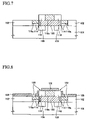
- a semiconductor device having a vertical gate will be described in detail with reference to FIG. 9 .
- a pair of first source/drain regions 106 are formed apart from each other by a predetermined distance in a silicon substrate 100 .
- a first silicon epitaxial layer 108 is formed on the pair of first source/drain regions 106 .
- a vertical gate insulation layer 114 is respectively formed at both sidewalls of the first silicon epitaxial layer 108 .
- the gate insulation layer 114 is horizontally elongated on the silicon substrate 100 .
- the gate insulation layer 114 is formed of silicon oxide.
- Second silicon epitaxial layers 116 a are respectively formed on the first silicon epitaxial layer 108 and on the gate insulation layer 114 .
- the second silicon epitaxial layer 116 a formed on the first silicon epitaxial layer 108 may be used as an electrode.
- a pair of second source/drain regions 118 are formed near both ends of the second silicon epitaxial layer 116 a formed on the first silicon epitaxial layer 108 .
- a vertical gate 124 is connectedly formed on the second source/drain regions 118 and on the second silicon epitaxial layer 116 a formed on the gate insulation layer 114 , respectively.
- the gate insulation layer 114 is horizontally elongated on the silicon substrate 100 under the second silicon epitaxial layer 116 a under the gate 124 .
- the gate 124 is formed as a silicide. Because such a gate 124 (and also the vertical gate insulation layer 114 ) is formed in a generally vertical shape, the integration capacity of semiconductor devices may be enhanced by employing such a structure.
- FIG. 1 to FIG. 9 are cross-sectional views showing sequential stages of a method of manufacturing the example semiconductor device having a vertical gate.
- a buffer oxide layer 102 is formed on the silicon substrate 100 .
- a mask pattern 104 partially exposing the buffer oxide layer 102 is formed thereon.
- the first source/drain regions 106 are formed apart from each other by a predetermined distance by ion implantation of source/drain impurities into the silicon substrate 100 with the use of the mask pattern 104 as an ion implantation mask.
- an n-type impurity for example, arsenic (As) or phosphorus (P) may be used as the source/drain impurity.
- a p-type impurity for example, boron (B) may be used as the source/drain impurity.
- the mask pattern 104 is removed. Then, a vertical transistor forming region 107 is formed by etching the buffer oxide layer 102 on the first source/drain regions 106 . Therefore, the vertical transistor forming region 107 is formed to expose the first source/drain regions 106 .
- the vertical transistor forming region 107 is filled with the first silicon epitaxial layer 108 .
- the first silicon epitaxial layer 108 may be formed by firstly forming a silicon epitaxial layer on the entire substrate 100 and then performing chemical mechanical polishing.
- a first insulation layer 110 is formed on the first silicon epitaxial layer 108 such that the first silicon epitaxial layer 108 may be protected thereby.
- the first insulation layer 110 is formed of silicon nitride.
- the first insulation layer 110 and the buffer oxide layer 102 are patterned such that vertical gate forming regions 112 are prepared at positions laterally exterior to the pair of first source/drain regions 106 .
- the gate insulation layers 114 are formed in the gate forming regions 112 .
- the gate insulation layers 114 are formed on the silicon substrate 100 and at both sidewalls of the first silicon epitaxial layer 108 . That is, the gate insulation layers 114 are vertically formed at both sidewalls of the first silicon epitaxial layer 108 .
- the gate insulation layers 114 are formed by oxidation of a surface of the silicon substrate 100 and both sidewalls of the first silicon epitaxial layer 108 .
- the gate insulation layers 114 are formed of silicon oxide.
- the first insulation layer 110 on the first silicon epitaxial layer 108 and the buffer oxide layer 102 is removed.
- an upper silicon epitaxial layer 116 is formed on the vertical gate forming region 112 , the first silicon epitaxial layer 108 , and the buffer oxide layer 102 .
- the upper silicon epitaxial layer 116 fills the gate forming region 112 that is formed in the shape of a hole.
- a pair of second source/drain regions 118 are formed by ion implantation of impurities into the upper silicon epitaxial layer 116 at positions vertically above the first source/drain regions 106 .
- the second silicon epitaxial layers 116 a are formed by etching the upper silicon epitaxial layer 116 exterior to the second source/drain regions 118 but leaving the upper silicon epitaxial layer 116 within the vertical gate forming regions 112 .
- the second silicon epitaxial layers 116 a remain on the first silicon epitaxial layer 108 and within the gate forming regions 112 above the gate insulation layers 114 .
- the second silicon epitaxial layers 116 a may be formed of polysilicon, and may be used as electrodes.
- a second insulation layer 120 having open regions 122 therein is formed such that the second silicon epitaxial layers 116 a in the vertical gate forming regions 112 as well as the second source/drain regions 118 are partly exposed at the open regions 122 .
- the second insulation layer 120 is formed of silicon nitride.
- the gate 124 is respectively formed at the open regions 122 .
- the gate 124 is formed as a silicide. Because such a gate 124 (and also the vertical gate insulation layer 114 ) is formed in a generally vertical shape, integration capacity of semiconductor devices may be enhanced.
- integration capacity of semiconductor devices may be enhanced because a gate (and also a vertical gate insulation layer) is formed in a generally vertical shape.
Landscapes
- Insulated Gate Type Field-Effect Transistor (AREA)
- Semiconductor Memories (AREA)
Abstract
Description
Claims (4)
Priority Applications (1)
| Application Number | Priority Date | Filing Date | Title |
|---|---|---|---|
| US11/607,328 US7312493B2 (en) | 2004-12-22 | 2006-11-30 | Semiconductor device and method of manufacturing the same |
Applications Claiming Priority (2)
| Application Number | Priority Date | Filing Date | Title |
|---|---|---|---|
| KR10-2004-0110627 | 2004-12-22 | ||
| KR1020040110627A KR100613287B1 (en) | 2004-12-22 | 2004-12-22 | Semiconductor device having vertical gate and manufacturing method thereof |
Related Child Applications (1)
| Application Number | Title | Priority Date | Filing Date |
|---|---|---|---|
| US11/607,328 Division US7312493B2 (en) | 2004-12-22 | 2006-11-30 | Semiconductor device and method of manufacturing the same |
Publications (2)
| Publication Number | Publication Date |
|---|---|
| US20060157715A1 US20060157715A1 (en) | 2006-07-20 |
| US7160778B2 true US7160778B2 (en) | 2007-01-09 |
Family
ID=36682955
Family Applications (2)
| Application Number | Title | Priority Date | Filing Date |
|---|---|---|---|
| US11/314,135 Expired - Fee Related US7160778B2 (en) | 2004-12-22 | 2005-12-21 | Semiconductor device and method of manufacturing the same |
| US11/607,328 Expired - Fee Related US7312493B2 (en) | 2004-12-22 | 2006-11-30 | Semiconductor device and method of manufacturing the same |
Family Applications After (1)
| Application Number | Title | Priority Date | Filing Date |
|---|---|---|---|
| US11/607,328 Expired - Fee Related US7312493B2 (en) | 2004-12-22 | 2006-11-30 | Semiconductor device and method of manufacturing the same |
Country Status (2)
| Country | Link |
|---|---|
| US (2) | US7160778B2 (en) |
| KR (1) | KR100613287B1 (en) |
Cited By (1)
| Publication number | Priority date | Publication date | Assignee | Title |
|---|---|---|---|---|
| US20080242029A1 (en) * | 2007-03-30 | 2008-10-02 | Chun-Tai Wu | Method and structure for making a top-side contact to a substrate |
Citations (2)
| Publication number | Priority date | Publication date | Assignee | Title |
|---|---|---|---|---|
| US20020109176A1 (en) | 2001-02-09 | 2002-08-15 | Micron Technology, Inc. | Open bit line dram with ultra thin body transistors |
| US20040113207A1 (en) | 2002-12-11 | 2004-06-17 | International Business Machines Corporation | Vertical MOSFET SRAM cell |
Family Cites Families (4)
| Publication number | Priority date | Publication date | Assignee | Title |
|---|---|---|---|---|
| CA2010068C (en) * | 1990-02-14 | 1993-10-26 | Steven Murray Hoxey | Partitioning case statements for optimal execution performance |
| US6076141A (en) * | 1996-01-24 | 2000-06-13 | Sun Microsytems, Inc. | Look-up switch accelerator and method of operating same |
| US6437389B1 (en) * | 2000-08-22 | 2002-08-20 | Micron Technology, Inc. | Vertical gate transistors in pass transistor programmable logic arrays |
| US6775763B2 (en) * | 2001-03-09 | 2004-08-10 | Koninklijke Philips Electronics N.V. | Bytecode instruction processor with switch instruction handling logic |
-
2004
- 2004-12-22 KR KR1020040110627A patent/KR100613287B1/en not_active Expired - Fee Related
-
2005
- 2005-12-21 US US11/314,135 patent/US7160778B2/en not_active Expired - Fee Related
-
2006
- 2006-11-30 US US11/607,328 patent/US7312493B2/en not_active Expired - Fee Related
Patent Citations (4)
| Publication number | Priority date | Publication date | Assignee | Title |
|---|---|---|---|---|
| US20020109176A1 (en) | 2001-02-09 | 2002-08-15 | Micron Technology, Inc. | Open bit line dram with ultra thin body transistors |
| KR20030088432A (en) | 2001-02-09 | 2003-11-19 | 마이크론 테크놀로지, 인크. | Open bit line dram with vertical ultra-thin body transistors |
| US20040113207A1 (en) | 2002-12-11 | 2004-06-17 | International Business Machines Corporation | Vertical MOSFET SRAM cell |
| KR20040051506A (en) | 2002-12-11 | 2004-06-18 | 인터내셔널 비지네스 머신즈 코포레이션 | Vertical mosfet sram cell |
Cited By (3)
| Publication number | Priority date | Publication date | Assignee | Title |
|---|---|---|---|---|
| US20080242029A1 (en) * | 2007-03-30 | 2008-10-02 | Chun-Tai Wu | Method and structure for making a top-side contact to a substrate |
| US7482645B2 (en) * | 2007-03-30 | 2009-01-27 | Fairchild Semiconductor Corporation | Method and structure for making a top-side contact to a substrate |
| US20090194812A1 (en) * | 2007-03-30 | 2009-08-06 | Chun-Tai Wu | Structure for Making a Top-side Contact to a Substrate |
Also Published As
| Publication number | Publication date |
|---|---|
| KR100613287B1 (en) | 2006-08-21 |
| US20060157715A1 (en) | 2006-07-20 |
| US7312493B2 (en) | 2007-12-25 |
| KR20060072229A (en) | 2006-06-28 |
| US20070075383A1 (en) | 2007-04-05 |
Similar Documents
| Publication | Publication Date | Title |
|---|---|---|
| US7772053B2 (en) | Method for fabrication of semiconductor device | |
| US11532637B2 (en) | Embedded flash memory cell including a tunnel dielectric layer having different thicknesses over a memory region | |
| US8344455B2 (en) | Semiconductor device and fabrication method for the same | |
| JP2012004473A (en) | Semiconductor device and method for manufacturing semiconductor device | |
| US20080220580A1 (en) | Semiconductor device and a method of manufacturing the same | |
| US7316945B2 (en) | Method of fabricating a fin field effect transistor in a semiconductor device | |
| USRE42180E1 (en) | Semiconductor device having metal silicide layer on source/drain region and gate electrode and method of manufacturing the same | |
| US10971596B2 (en) | Semiconductor device with reduced flicker noise | |
| US8598004B2 (en) | Self aligned MOS structure with polysilicon contact | |
| US7626224B2 (en) | Semiconductor device with split gate memory cell and fabrication method thereof | |
| KR101974391B1 (en) | Methods of forming integrated circuit devices using self-aligned contact formation techniques | |
| US7696025B2 (en) | Sidewall semiconductor transistors | |
| US7160778B2 (en) | Semiconductor device and method of manufacturing the same | |
| TW564496B (en) | Semiconductor device and method of manufacturing the same | |
| KR20140012864A (en) | Semiconductor device and method for manufacturing the same | |
| US7714380B2 (en) | Semiconductor device and method of manufacturing the semiconductor device | |
| JP2007027348A (en) | Semiconductor device and manufacturing method thereof | |
| US8664063B2 (en) | Method of producing a semiconductor device and semiconductor device | |
| KR100670395B1 (en) | Manufacturing Method of Semiconductor Device | |
| JP2008311675A (en) | Semiconductor device | |
| KR101087782B1 (en) | Semiconductor device and manufacturing method thereof | |
| US20050170620A1 (en) | Transistors for semiconductor device and methods of fabricating the same | |
| KR100562330B1 (en) | A MOS transistor having a vertical oxide film as an isolation film and a method of manufacturing the same | |
| KR20060099214A (en) | CMOS transistors in semiconductor devices and methods of forming the | |
| KR20100078983A (en) | Semiconductor device having recess gate and method of fabricating the same |
Legal Events
| Date | Code | Title | Description |
|---|---|---|---|
| AS | Assignment |
Owner name: DONGBUANAM SEMICONDUCTOR, INC., KOREA, REPUBLIC OF Free format text: ASSIGNMENT OF ASSIGNORS INTEREST;ASSIGNOR:LIM, TAE-HONG;REEL/FRAME:017404/0051 Effective date: 20051220 |
|
| AS | Assignment |
Owner name: DONGBU ELECTRONICS CO., LTD.,KOREA, REPUBLIC OF Free format text: CHANGE OF NAME;ASSIGNOR:DONGANAM SEMICONDUCTOR INC.;REEL/FRAME:017749/0335 Effective date: 20060328 Owner name: DONGBU ELECTRONICS CO., LTD., KOREA, REPUBLIC OF Free format text: CHANGE OF NAME;ASSIGNOR:DONGANAM SEMICONDUCTOR INC.;REEL/FRAME:017749/0335 Effective date: 20060328 |
|
| AS | Assignment |
Owner name: DONGBU ELECTRONICS CO., LTD., KOREA, REPUBLIC OF Free format text: CORRECTIVE ASSIGNMENT TO CORRECT THE ASSIGNOR PREVIOUSLY RECORDED ON REEL 017749 FRAME 0335;ASSIGNOR:DONGBUANAM SEMICONDUCTOR INC.;REEL/FRAME:017821/0670 Effective date: 20060328 Owner name: DONGBU ELECTRONICS CO., LTD.,KOREA, REPUBLIC OF Free format text: CORRECTIVE ASSIGNMENT TO CORRECT THE ASSIGNOR PREVIOUSLY RECORDED ON REEL 017749 FRAME 0335. ASSIGNOR(S) HEREBY CONFIRMS THE ASSIGNOR SHOULD BE "DONGBUANAM SEMICONDUCTOR INC.";ASSIGNOR:DONGBUANAM SEMICONDUCTOR INC.;REEL/FRAME:017821/0670 Effective date: 20060328 Owner name: DONGBU ELECTRONICS CO., LTD., KOREA, REPUBLIC OF Free format text: CORRECTIVE ASSIGNMENT TO CORRECT THE ASSIGNOR PREVIOUSLY RECORDED ON REEL 017749 FRAME 0335. ASSIGNOR(S) HEREBY CONFIRMS THE ASSIGNOR SHOULD BE "DONGBUANAM SEMICONDUCTOR INC.";ASSIGNOR:DONGBUANAM SEMICONDUCTOR INC.;REEL/FRAME:017821/0670 Effective date: 20060328 |
|
| FEPP | Fee payment procedure |
Free format text: PAYOR NUMBER ASSIGNED (ORIGINAL EVENT CODE: ASPN); ENTITY STATUS OF PATENT OWNER: LARGE ENTITY |
|
| FPAY | Fee payment |
Year of fee payment: 4 |
|
| REMI | Maintenance fee reminder mailed | ||
| LAPS | Lapse for failure to pay maintenance fees | ||
| STCH | Information on status: patent discontinuation |
Free format text: PATENT EXPIRED DUE TO NONPAYMENT OF MAINTENANCE FEES UNDER 37 CFR 1.362 |
|
| STCH | Information on status: patent discontinuation |
Free format text: PATENT EXPIRED DUE TO NONPAYMENT OF MAINTENANCE FEES UNDER 37 CFR 1.362 |
|
| FP | Lapsed due to failure to pay maintenance fee |
Effective date: 20150109 |