US7157754B2 - Solid-state imaging device and interline transfer CCD image sensor - Google Patents
Solid-state imaging device and interline transfer CCD image sensor Download PDFInfo
- Publication number
- US7157754B2 US7157754B2 US10/742,419 US74241903A US7157754B2 US 7157754 B2 US7157754 B2 US 7157754B2 US 74241903 A US74241903 A US 74241903A US 7157754 B2 US7157754 B2 US 7157754B2
- Authority
- US
- United States
- Prior art keywords
- photodiode
- conductivity type
- well
- deep
- semiconductor substrate
- Prior art date
- Legal status (The legal status is an assumption and is not a legal conclusion. Google has not performed a legal analysis and makes no representation as to the accuracy of the status listed.)
- Expired - Fee Related, expires
Links
Images


Classifications
-
- H—ELECTRICITY
- H10—SEMICONDUCTOR DEVICES; ELECTRIC SOLID-STATE DEVICES NOT OTHERWISE PROVIDED FOR
- H10F—INORGANIC SEMICONDUCTOR DEVICES SENSITIVE TO INFRARED RADIATION, LIGHT, ELECTROMAGNETIC RADIATION OF SHORTER WAVELENGTH OR CORPUSCULAR RADIATION
- H10F39/00—Integrated devices, or assemblies of multiple devices, comprising at least one element covered by group H10F30/00, e.g. radiation detectors comprising photodiode arrays
- H10F39/80—Constructional details of image sensors
- H10F39/803—Pixels having integrated switching, control, storage or amplification elements
-
- H—ELECTRICITY
- H10—SEMICONDUCTOR DEVICES; ELECTRIC SOLID-STATE DEVICES NOT OTHERWISE PROVIDED FOR
- H10F—INORGANIC SEMICONDUCTOR DEVICES SENSITIVE TO INFRARED RADIATION, LIGHT, ELECTROMAGNETIC RADIATION OF SHORTER WAVELENGTH OR CORPUSCULAR RADIATION
- H10F39/00—Integrated devices, or assemblies of multiple devices, comprising at least one element covered by group H10F30/00, e.g. radiation detectors comprising photodiode arrays
- H10F39/10—Integrated devices
- H10F39/12—Image sensors
- H10F39/18—Complementary metal-oxide-semiconductor [CMOS] image sensors; Photodiode array image sensors
-
- H—ELECTRICITY
- H10—SEMICONDUCTOR DEVICES; ELECTRIC SOLID-STATE DEVICES NOT OTHERWISE PROVIDED FOR
- H10F—INORGANIC SEMICONDUCTOR DEVICES SENSITIVE TO INFRARED RADIATION, LIGHT, ELECTROMAGNETIC RADIATION OF SHORTER WAVELENGTH OR CORPUSCULAR RADIATION
- H10F39/00—Integrated devices, or assemblies of multiple devices, comprising at least one element covered by group H10F30/00, e.g. radiation detectors comprising photodiode arrays
- H10F39/011—Manufacture or treatment of image sensors covered by group H10F39/12
-
- H—ELECTRICITY
- H10—SEMICONDUCTOR DEVICES; ELECTRIC SOLID-STATE DEVICES NOT OTHERWISE PROVIDED FOR
- H10F—INORGANIC SEMICONDUCTOR DEVICES SENSITIVE TO INFRARED RADIATION, LIGHT, ELECTROMAGNETIC RADIATION OF SHORTER WAVELENGTH OR CORPUSCULAR RADIATION
- H10F39/00—Integrated devices, or assemblies of multiple devices, comprising at least one element covered by group H10F30/00, e.g. radiation detectors comprising photodiode arrays
- H10F39/80—Constructional details of image sensors
- H10F39/803—Pixels having integrated switching, control, storage or amplification elements
- H10F39/8037—Pixels having integrated switching, control, storage or amplification elements the integrated elements comprising a transistor
-
- H—ELECTRICITY
- H10—SEMICONDUCTOR DEVICES; ELECTRIC SOLID-STATE DEVICES NOT OTHERWISE PROVIDED FOR
- H10F—INORGANIC SEMICONDUCTOR DEVICES SENSITIVE TO INFRARED RADIATION, LIGHT, ELECTROMAGNETIC RADIATION OF SHORTER WAVELENGTH OR CORPUSCULAR RADIATION
- H10F39/00—Integrated devices, or assemblies of multiple devices, comprising at least one element covered by group H10F30/00, e.g. radiation detectors comprising photodiode arrays
- H10F39/80—Constructional details of image sensors
- H10F39/807—Pixel isolation structures
-
- H—ELECTRICITY
- H10—SEMICONDUCTOR DEVICES; ELECTRIC SOLID-STATE DEVICES NOT OTHERWISE PROVIDED FOR
- H10W—GENERIC PACKAGES, INTERCONNECTIONS, CONNECTORS OR OTHER CONSTRUCTIONAL DETAILS OF DEVICES COVERED BY CLASS H10
- H10W10/00—Isolation regions in semiconductor bodies between components of integrated devices
- H10W10/01—Manufacture or treatment
- H10W10/011—Manufacture or treatment of isolation regions comprising dielectric materials
- H10W10/014—Manufacture or treatment of isolation regions comprising dielectric materials using trench refilling with dielectric materials, e.g. shallow trench isolations
- H10W10/0148—Manufacture or treatment of isolation regions comprising dielectric materials using trench refilling with dielectric materials, e.g. shallow trench isolations comprising introducing impurities in side walls or bottom walls of trenches, e.g. for forming channel stoppers
-
- H—ELECTRICITY
- H10—SEMICONDUCTOR DEVICES; ELECTRIC SOLID-STATE DEVICES NOT OTHERWISE PROVIDED FOR
- H10W—GENERIC PACKAGES, INTERCONNECTIONS, CONNECTORS OR OTHER CONSTRUCTIONAL DETAILS OF DEVICES COVERED BY CLASS H10
- H10W10/00—Isolation regions in semiconductor bodies between components of integrated devices
- H10W10/10—Isolation regions comprising dielectric materials
- H10W10/17—Isolation regions comprising dielectric materials formed using trench refilling with dielectric materials, e.g. shallow trench isolations
-
- H—ELECTRICITY
- H10—SEMICONDUCTOR DEVICES; ELECTRIC SOLID-STATE DEVICES NOT OTHERWISE PROVIDED FOR
- H10F—INORGANIC SEMICONDUCTOR DEVICES SENSITIVE TO INFRARED RADIATION, LIGHT, ELECTROMAGNETIC RADIATION OF SHORTER WAVELENGTH OR CORPUSCULAR RADIATION
- H10F39/00—Integrated devices, or assemblies of multiple devices, comprising at least one element covered by group H10F30/00, e.g. radiation detectors comprising photodiode arrays
- H10F39/10—Integrated devices
- H10F39/12—Image sensors
- H10F39/15—Charge-coupled device [CCD] image sensors
- H10F39/153—Two-dimensional or three-dimensional array CCD image sensors
- H10F39/1534—Interline transfer
-
- H—ELECTRICITY
- H10—SEMICONDUCTOR DEVICES; ELECTRIC SOLID-STATE DEVICES NOT OTHERWISE PROVIDED FOR
- H10F—INORGANIC SEMICONDUCTOR DEVICES SENSITIVE TO INFRARED RADIATION, LIGHT, ELECTROMAGNETIC RADIATION OF SHORTER WAVELENGTH OR CORPUSCULAR RADIATION
- H10F39/00—Integrated devices, or assemblies of multiple devices, comprising at least one element covered by group H10F30/00, e.g. radiation detectors comprising photodiode arrays
- H10F39/80—Constructional details of image sensors
Definitions
- the present invention relates to a solid-state imaging device provided with an element isolation portion formed of a STI (Shallow Trench Isolation) that is a grooved portion of a semiconductor substrate and a method for manufacturing the same and relates to an interline transfer CCD image sensor.
- STI Shallow Trench Isolation
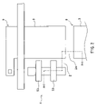
- FIG. 6 is a circuit diagram showing a configuration of a conventional solid-state imaging device 90 .
- the solid-state imaging device 90 includes a plurality of pixel cells 99 arranged in a matrix form on a semiconductor substrate 10 .
- Each of the pixel cells 99 includes a photodiode 93 that converts incident light into a signal charge and stores the signal charge.
- a transfer transistor 94 for reading out the signal charge stored in the photodiode 93 is provided.
- Each of the pixel cells 99 includes an amplify transistor 12 .
- the amplify transistor 12 amplifies the signal charge read out by the transfer transistor 94 .
- a reset transistor 11 is provided in each of the pixel cells 99 . The reset transistor 11 resets the signal charge read out by the transfer transistor 94 .
- the solid-state imaging device 90 includes a vertical driving circuit 15 .
- a plurality of reset transistor control lines 111 are connected to the vertical driving circuit 15 .
- the reset transistor control lines 111 are arranged parallel with each other at predetermined intervals and along a horizontal direction so as to be connected to the reset transistors 11 that are respectively provided in the pixel cells 99 arranged along the horizontal direction.
- a plurality of vertical select transistor control lines 121 further are connected to the vertical driving circuit 15 .
- the vertical select transistor control lines 121 are arranged parallel with each other at predetermined intervals and along the horizontal direction so as to be connected to vertical select transistors that are provided respectively in the pixel cells 99 arranged along the horizontal direction.
- the vertical select transistor control lines 121 determine a row from which a signal is to be read out.
- a source of each vertical select transistor is connected to a vertical signal line 61 .
- a load transistor group 27 is connected to one end of each vertical signal line 61 .
- the other end of each vertical signal line 61 is connected to a row signal storing portion 28 .
- the row signal storing portion 28 includes a switching transistor for capturing signals from one row.
- a horizontal driving circuit 16 is connected to the row signal storing portion 28 .
- FIG. 7 is a timing chart for explaining an operation of the conventional solid-state imaging device 90 .
- a reset pulse 102 - 1 for making a reset transistor control line 111 at a high level is applied so as to reset a potential of a floating diffusion layer to which a gate of each of the amplify transistors 12 is connected.
- a transfer pulse 103 - 1 is applied so as to make a level of transfer transistor control lines high, which allows a signal charge stored in each of the photodiodes 93 to be transferred to the floating diffusion layer.
- each of the amplify transistors 12 connected to the floating diffusion layer has a gate voltage equal to the potential of the floating diffusion layer, which allows a voltage that is substantially equal to this gate voltage to appear across the vertical signal line 61 . Then, a signal based on the signal charge stored in the photodiode 93 is transferred to the row signal storing portion 28 .
- the horizontal driving circuit 16 sequentially generates column selection pulses 106 - 1 - 1 , 106 - 1 - 2 , . . . so as to extract the signals that have been transferred to the row signal storing portion 28 as an output signal 107 - 1 corresponding to those obtained from one row.
- FIG. 8 is a plan view for explaining a configuration of the photodiode 93 and the transfer transistor 94 that are provided in the conventional solid-state imaging device 90 .
- FIG. 9 is a cross-sectional view taken along a line AA shown in FIG. 8 .
- the photodiode 93 is a buried-type pnp photodiode that includes a surface shield layer 85 formed at a surface of a semiconductor substrate 10 and a storage photodiode layer 86 formed below the surface shield layer 85 .
- the surface shield layer 85 has a conductivity type opposite to that of the semiconductor substrate 10 and the storage photodiode layer 86 has the same conductivity type as that of the semiconductor substrate 10 .
- the storage photodiode layer 86 is formed at a position of about 1 ⁇ m in depth.
- the transfer transistor 94 is formed adjacent to the photodiode 93 and includes a gate electrode 53 formed on the semiconductor substrate 10 and a source 87 and a drain 88 formed on each side of the gate electrode 53 .
- an element isolation portion 2 formed of a STI (Shallow Trench Isolation), which is a grooved portion of the semiconductor substrate 10 is formed so that the photodiode 93 and the transfer transistor 94 are isolated from each other.
- STI Shallow Trench Isolation
- An element isolation portion 2 A is formed so that the photodiode 93 is isolated from another photodiode 93 contained in a pixel cell 99 adjacent to the pixel cell 99 containing the photodiode 93 .
- the element isolation portion 2 and the element isolation portion 2 A are formed at up to a depth of about 300 nm. As the microfabrication of transistors proceeds, the element isolation portion 2 and the element isolation portion 2 A are increasingly made shallower. This is because as the microfabrication proceeds, the width of the element isolation portion becomes narrower rapidly, and if the element isolation portion is grooved deeply, its aspect ratio becomes large, which makes it impossible to fill an oxidation film in that portion.
- the storage photodiode layer 86 of the photodiode 93 is formed at a position deeper than the element isolation portion 2 and the element isolation portion 2 A.
- FIG. 10 is a cross-sectional view along the line AA shown in FIG. 8 for explaining configurations of a photodiode and a MOS transistor that are provided in another conventional solid-state imaging device.
- the same reference numerals are assigned to the elements having the same configurations as those of the elements described with reference to FIG. 9 , and therefore detailed explanations for these elements will be omitted.
- a p-type well 202 is formed on an n-type semiconductor substrate 201 .
- a depth of an interface between the n-type semiconductor substrate 201 and the p-type well 202 is set at about 2.8 ⁇ m.
- a density of the n-type semiconductor substrate 201 is set at about 2 ⁇ 10 14 cm ⁇ 3 and a density of the p-type well 202 is set at about 1 ⁇ 10 15 cm ⁇ 3 .
- a charge stored in the photodiode 93 is discharged directly to the semiconductor substrate 201 as indicated by an arrow 203 .
- This well structure can prevent a charge occurring at a deeper portion of the substrate also from reaching to the photodiode 93 and to the transfer transistor 94 .
- the signal charge stored in the storage photodiode layer 86 flows beyond the element isolation portion 2 A and into the adjacent photodiode 93 as indicated by an arrow 82 .
- the signal charge stored in the storage photodiode layer 86 flows beyond the element isolation portion 2 A and into the adjacent photodiode 93 as indicated by an arrow 82 .
- there is a problem of a phenomenon called color mixture which degrades the reproducibility of colors by the imaging device.
- a divide 204 is formed at a position of about 1.8 ⁇ m in depth that is around the midpoint between the lower end of the p-type well 202 and the lower end of the storage photodiode layer 86 . Although a charge occurring at a position shallower than the divide 204 arrives at the photodiode 93 , a charge occurring at a position deeper than the divide 204 does not arrive at the photodiode 93 , which degrades the sensitivity.
- the divide 204 represents a virtual border line between an electron flowing on a surface side due to thermal diffusion in terms of probabilities and an electron flowing through a deep portion of the substrate.
- a depletion layer that extends from a side of the photodiode 93 toward the semiconductor substrate 201 through the p-type well 202 and a depletion layer that extends from the n-type semiconductor substrate 201 toward the photodiode 93 through the p-type well 202 contact with each other at the divide 204 .
- a charge overflowing the saturated photodiode 93 passes through the depletion layer to which an electric field is applied, and therefore the charge is discharged along the electric field to the n-type semiconductor substrate 201 without moving randomly.
- This is the same operation as in a well-known interline transfer type vertical overflow drain structure in which each pixel cell unit has a photodiode and a vertical CCD.
- Such a discharge method is called a junction FET mode.
- a solid-state imaging device includes: a plurality of pixel cells arranged in a matrix form on a semiconductor substrate; and a driving unit that is provided for driving the plurality of pixel cells.
- Each of the plurality of pixel cells includes: a photodiode that converts incident light into a signal charge and stores the signal charge; at least one MOS transistor that is provided for reading out the signal charge stored in the photodiode; an element isolation portion, which is formed of a STI (Shallow Trench Isolation) that is a grooved portion of the semiconductor substrate so that the photodiode and the MOS transistor are isolated from each other; and a deep-portion isolation implantation layer that is formed under the element isolation portion for preventing a flow of a charge from the photodiode to the MOS transistor.
- STI Shallow Trench Isolation
- Another solid-state imaging device includes: a plurality of pixel cells arranged in a matrix form on a semiconductor substrate; and a driving unit that is provided for driving the plurality of pixel cells.
- Each of the plurality of pixel cells includes: a photodiode that converts incident light into a signal charge and stores the signal charge; at least one MOS transistor that is provided for reading out the signal charge stored in the photodiode; an element isolation portion that is formed of a STI (Shallow Trench Isolation), which is a grooved portion of the semiconductor substrate so that the photodiode and another photodiode included in a pixel cell adjacent to the pixel cell including the photodiode are isolated from each other; and a deep-portion isolation implantation layer that is formed under the element isolation portion for preventing a flow of a charge from the photodiode to another photodiode included in a pixel cell adjacent to the pixel cell including the photodiode.
- STI Shallow Trench Isolation
- a solid-state imaging device manufacturing method is for manufacturing the solid-state imaging device according to the present invention and includes the steps of: grooving the semiconductor substrate so as to form a groove for the formation of the element isolation portion; implanting an impurity from a bottom of the groove so as to form the deep-portion isolation implantation layer for preventing a flow of a charge from the photodiode to the MOS transistor; forming the element isolation portion in the groove after the impurity implantation step; and forming the photodiode and the at least one MOS transistor after the element isolation portion formation step.
- An interline transfer CCD image sensor includes: a plurality of pixel cells arranged in a matrix form on a semiconductor substrate; and a driving unit that is provided for driving the plurality of pixel cells.
- Each of the plurality of pixel cells includes: a photodiode that converts incident light into a signal charge and stores the signal charge; a transfer gate that is provided for reading out the signal charge stored in the photodiode; an element isolation portion, which is formed of a STI (Shallow Trench Isolation) that is a grooved portion of the semiconductor substrate so that the photodiode and the transfer gate are isolated from each other; vertical transfer CCDs that are arranged at predetermined intervals and along a vertical direction so as to be adjacent to the respective pixel cells that are arranged along a column direction, the vertical transfer CCDs being provided for transferring the signal charge read out from the photodiode by the transfer gate along the vertical direction; and a deep-portion isolation implantation layer that is formed under the element isolation portion for preventing
- FIG. 1 is a circuit diagram showing a configuration of a solid-state imaging device according to the present embodiment.
- FIG. 2 is a plan view for explaining a configuration of a photodiode and a MOS transistor that are provided in the solid-state imaging device according to this embodiment.
- FIG. 3 is a cross-sectional view taken along a line AA shown in FIG. 2 .
- FIG. 4 is a cross-sectional view taken along a line AA shown in FIG. 2 for explaining a configuration of a photodiode and a MOS transistor that are provided in another solid-state imaging device according to this embodiment.
- FIG. 5 is a plan view for explaining a configuration of an interline transfer CCD image sensor according to this embodiment.
- FIG. 6 is a circuit diagram showing a configuration of the conventional solid-state imaging device.
- FIG. 7 is a timing chart for explaining an operation of the conventional solid-state imaging device.
- FIG. 8 is a plan view for explaining a configuration of a photodiode and a MOS transistor that are provided in the conventional solid-state imaging device.
- FIG. 9 is a cross-sectional view taken along a line AA shown in FIG. 8 .
- FIG. 10 is a cross-sectional view taken along a line AA shown in FIG. 8 for explaining a configuration of a photodiode and a MOS transistor that are provided in another conventional solid-state imaging device.
- the deep-portion isolation implantation layer is formed under the element isolation portion for preventing a flow of a charge from the photodiode to the MOS transistor. Therefore, the flow of a charge from the photodiode to the MOS transistor can be prevented. As a result, a solid-state imaging device with a favorable sensitivity can be obtained.
- the MOS transistor includes a source and a drain that are formed in the semiconductor substrate, and an impurity having a conductivity type opposite to a conductivity type of the source and the drain of the MOS transistor is implanted into the deep-portion isolation implantation layer.
- the element isolation portion is formed so that the photodiode is isolated from another photodiode included in a pixel cell adjacent to the pixel cell including the photodiode, and the deep-portion isolation implantation layer is formed so as to prevent a flow of a charge from the photodiode to another photodiode included in a pixel cell adjacent to the pixel cell including the photodiode.
- the deep-portion isolation implantation layer is formed to a position deeper than the photodiode.
- the deep-portion isolation implantation layer is formed at a position from about 0.3 ⁇ m to about 1.0 ⁇ m in depth from a surface of the semiconductor substrate.
- the photodiode includes: a surface shield layer that is formed at a surface of the semiconductor substrate; and a storage photodiode layer that is formed under the surface shield layer, wherein a density of the deep-portion isolation implantation layer is larger than a density of the storage photodiode layer.
- the at least one MOS transistor is at least one n-type MOS transistor.
- the semiconductor substrate includes: a first p-type well that is formed so as to enclose the photodiode, the element isolation portion and side faces and a bottom face of the deep-portion isolation implantation layer; and a second p-type well that is formed under the first p-type well and has an impurity density higher than an impurity density of the first p-type well.
- the deep-portion isolation implantation layer is formed so as to contact with the second p-type well.
- an impurity density of the deep-portion isolation implantation layer is larger than the impurity density of the second p-type well.
- the driving unit includes: a vertical driving circuit for driving the plurality of pixel cells along a row direction; and a horizontal driving circuit for driving the plurality of pixel cells along a column direction.
- the deep-portion isolation implantation layer is formed under the element isolation portion for preventing a flow of a charge from the photodiode to another photodiode included in a pixel cell adjacent to the pixel cell including the photodiode. Therefore, the flow of a charge from the photodiode to another photodiode included in a pixel cell adjacent to the pixel cell including the photodiode can be prevented. As a result, a solid-state imaging device with a favorable sensitivity can be obtained.
- an impurity is implanted from a bottom of the groove so as to form the deep-portion isolation implantation layer for preventing a flow of a charge from the photodiode to the MOS transistor. Therefore, the thus formed deep-portion isolation implantation layer can prevent the flow of a charge from the photodiode to the MOS transistor. As a result, a solid-state imaging device with a favorable sensitivity can be manufactured.
- the deep-portion isolation implantation layer is formed under the element isolation portion for preventing a flow of a charge from the photodiode to the transfer gate. Therefore, the flow of a charge from the photodiode to the transfer gate can be prevented. As a result, an interline transfer CCD image sensor with a favorable sensitivity can be obtained.
- the semiconductor substrate includes: a first p-type well that is formed so as to enclose the photodiode, the element isolation portion and side faces and a bottom face of the deep-portion isolation implantation layer; and a second p-type well that is formed under the first p-type well and has an impurity density higher than an impurity density of the first p-type well.
- the deep-portion isolation implantation layer is formed so as to contact with the second p-type well.
- an impurity density of the deep-portion isolation implantation layer is larger than the impurity density of the second p-type well.
- FIG. 1 is a circuit diagram showing a configuration of a solid-state imaging device 100 according to this embodiment.
- the solid-state imaging device 100 includes a plurality of pixel cells 9 that are arranged in a matrix form on a semiconductor substrate 10 .
- Each of the pixel cells 9 includes a photodiode 3 that converts incident light into a signal charge and stores the signal charge.
- a transfer transistor 4 for reading out the signal charge stored in the photodiode 3 is provided.
- Each of the pixel cells 9 includes an amplify transistor 12 .
- the amplify transistor 12 amplifies the signal charge read out by the transfer transistor 4 .
- a reset transistor 11 is provided in each of the pixel cells 9 . The reset transistor 11 resets the signal charge read out by the transfer transistor 4 .
- the solid-state imaging device 100 includes a vertical driving circuit 15 .
- a plurality of reset transistor control lines 111 are connected to the vertical driving circuit 15 .
- the reset transistor control lines 111 are arranged parallel with each other at predetermined intervals and along a horizontal direction so as to be connected to the reset transistors 11 that are respectively provided in the pixel cells 9 arranged along the horizontal direction.
- a plurality of vertical select transistor control lines 121 further are connected to the vertical driving circuit 15 .
- the vertical select transistor control lines 121 are arranged parallel with each other at predetermined intervals and along the horizontal direction so as to be connected to vertical select transistors that are provided respectively in the pixel cells 9 arranged along the horizontal direction.
- the vertical select transistor control lines 121 determine a row from which a signal is to be read out.
- a source of each vertical select transistor is connected to a vertical signal line 61 .
- a load transistor group 27 is connected to one end of each vertical signal line 61 .
- the other end of each vertical signal line 61 is connected to a row signal storing portion 28 .
- the row signal storing portion 28 includes a switching transistor for capturing signals from one row.
- a horizontal driving circuit 16 is connected to the row signal storing portion 28 .
- FIG. 2 is a plan view for explaining a configuration of the photodiode 3 and the transfer transistor 4 that are provided in the solid-state imaging device 100 according to this embodiment.
- FIG. 3 is a cross-sectional view taken along a line AA shown in FIG. 2 .
- the photodiode 3 is a buried-type pnp photodiode that includes a surface shield layer 5 formed at a surface of a semiconductor substrate 10 and a storage photodiode layer 6 formed below the surface shield layer 5 .
- the surface shield layer 5 has a conductivity type opposite to that of the semiconductor substrate 10 and the storage photodiode layer 6 has the same conductivity type as that of the semiconductor substrate 10 .
- the surface shield layer 5 is formed at up to a position of about 0.2 ⁇ m in depth and the storage photodiode layer 6 is formed at up to a position of about 0.8 ⁇ m in depth.
- the transfer transistor 4 is formed adjacent to the photodiode 3 and includes a gate electrode 53 formed on the semiconductor substrate 10 and a source 7 and a drain 8 formed on each side of the gate electrode 53 .
- an element isolation portion 2 formed of a STI (Shallow Trench Isolation) that is a grooved portion of the semiconductor substrate 10 is formed so that the photodiode 3 and the transfer transistor 4 are isolated from each other.
- STI Shallow Trench Isolation
- An element isolation portion 2 A is formed so that the photodiode 3 is isolated from another photodiode 3 contained in a pixel cell 9 adjacent to the pixel cell 9 containing the photodiode 3 .
- the element isolation portion 2 and the element isolation portion 2 A are formed at up to a depth of about 300 nm. As the microfabrication of transistors proceeds, the element isolation portion 2 and the element isolation portion 2 A are increasingly made shallower. This is because as the microfabrication proceeds, the width of the element isolation portion becomes narrower rapidly, and if the element isolation portion is grooved deeply, its aspect ratio becomes large, which makes it impossible to fill an oxidation film in that portion.
- deep-portion isolation implantation layers 1 respectively are formed along a direction perpendicular to a surface of the semiconductor substrate 10 .
- the deep-portion isolation implantation layers 1 respectively are formed for preventing the flow of a charge from the photodiode 3 to the transfer transistor 4 and for preventing the flow of a charge from the photodiode 3 to another photodiode 3 included in a pixel cell 9 adjacent to the pixel cell 9 including the photodiode 3 .
- the deep-portion isolation implantation layers 1 are formed at positions from about 0.3 ⁇ m to about 1.0 ⁇ m in depth from the surface of the semiconductor substrate 10 . In this way, the deep-portion isolation implantation layers 1 are formed to positions deeper than the storage photodiode layer 6 of the photodiode 3 .
- An implantation density of the deep-portion isolation implantation layers 1 is set at 1 ⁇ 10 16 cm ⁇ 3 or more.
- a density of the surface shield layer 5 of the photodiode 3 is set at about 1 ⁇ 10 19 cm ⁇ 3 and a density of the storage photodiode layer 6 is set at about 1 ⁇ 10 17 cm ⁇ 3 .
- a density of the semiconductor substrate is set at 1 ⁇ 10 15 cm ⁇ 3 . In this way, the density of the deep-portion isolation implantation layers 1 is set larger than the density of the storage photodiode layer 6 .
- the semiconductor substrate 10 is grooved by etching to form grooves.
- boron B +11 is implanted from a bottom of the formed grooves under conditions of an acceleration voltage between 300 keV and 1 MeV, inclusive, and a dose between 5 ⁇ 10 11 cm ⁇ 2 and 1 ⁇ 10 12 cm ⁇ 2 , inclusive.
- the deep-portion isolation implantation layers 1 having an impurity density of 1 ⁇ 10 16 cm ⁇ 3 or more can be formed under the grooves.
- the grooves are filled with SiO 2 in accordance with a CVD method. Thereafter, the photodiode 3 and the transfer transistor 4 are formed in the semiconductor substrate 10 .
- the deep-portion isolation implantation layers 1 prevent the flow of the signal charge stored in the storage photodiode layer 6 into the transfer transistor 4 and the adjacent photodiode 3 .
- a generated charge 79 that has been converted photoelectrically at a deep portion of the semiconductor substrate 10 also is reflected from the deep-portion isolation implantation layers 1 , and therefore the flow of this charge into the adjacent transfer transistor 4 can be prevented. As a result, the sensitivity of the solid-state imaging device 100 is improved.
- the deep-portion isolation implantation layers 1 may be formed under all of the element isolation portions formed in the solid-state imaging device, in addition to under the element isolation portions around the photodiode 3 .
- the present invention is especially effective for the application to an nMOS sensor in which a solid-state imaging device is configured with nMOS transistors only, because such sensor has only one type of element isolation portion.
- the deep-portion isolation implantation layer 1 is formed under the element isolation portion 2 .
- the flow of the charge from the photodiode 3 to the MOS transistor 4 can be prevented.
- a solid-state imaging device with a favorable sensitivity can be obtained.
- FIG. 4 is a cross-sectional view for explaining a configuration of a photodiode 3 and a transfer transistor 4 that are provided in another solid-state imaging device according to this embodiment.
- the same reference numerals are assigned to the elements having the same configurations as those of the elements described with reference to FIG. 3 , and therefore detailed explanations for these elements will be omitted.
- a first p-type well 21 and a second p-type well 22 are provided in the semiconductor substrate 10 A.
- the first p-type well 21 is formed so as to enclose the photodiode 3 , element isolation portions 2 and 2 A and side faces and a bottom face of a deep-portion isolation implantation layer 1 .
- the second p-type well 22 is formed under the first p-type well 21 and has an impurity density higher than an impurity density of the first p-type well 21 .
- An impurity density of the n-type semiconductor substrate 10 A is set at 1 ⁇ 10 14 cm ⁇ 3 .
- the impurity density of the first p-type well 21 is set at 1 ⁇ 10 15 cm ⁇ 3 and the impurity density of the second p-type well 22 is set at 3 ⁇ 10 15 cm ⁇ 3 or more.
- An impurity density of the deep-portion isolation implantation layer 1 is set at 1 ⁇ 10 16 cm ⁇ 3 or more. In this way, the impurity density of the deep-portion isolation implantation layer 1 is set larger than the impurity density of the second p-type well 22 .
- the impurity density of the second p-type well 22 is set sufficiently higher than the impurity density of the first p-type well 21 .
- the first p-type well 21 is formed at up to a position of about 2.6 ⁇ m in depth from a surface of the semiconductor substrate 10 A.
- the second p-type well 22 is formed at a position between about 2.6 ⁇ m and about 3.0 ⁇ m in depth.
- a divide 204 of a charge is formed at substantially a midpoint of the second p-type well 22 . Therefore, the divide 204 is formed at a position deeper than the conventional divide described above with reference to FIG. 9 . That is to say, a region for storing a signal charge that has been converted by the photodiode 3 is widened.
- the provision of a deep-portion isolation implantation layer 1 in such a configuration allows the flow of a charge from the photodiode 3 to the transfer transistor 4 to be prevented. Thus, a saturation signal charge of the photodiode 3 increases.
- color mixture resulting from a generated charge 79 that has been converted photoelectrically at a deeper portion of the semiconductor substrate 10 A further can be suppressed, so that a solid-state imaging device with a favorable color reproducibility can be realized.
- the impurity density of the second p-type well 22 is higher than the impurity density of the n-type semiconductor substrate 10 A, a depletion layer extending from the n-type semiconductor substrate 10 A toward a side of the photodiode 3 stops at the second p-type well 22 . Therefore, the depletion layer cannot contact with a depletion layer extending from the photodiode 3 side toward a side of the n-type semiconductor substrate 10 A.
- a charge (electron) overflowing the photodiode 3 is emitted to a p-type neutral region in which a lot of holes are present.
- the electron emitted from the photodiode 3 to the p-type neutral region has a long life and never recombine with a hole, so as to move at random like the trace of a drunken gait in a region where an electric field does not act.
- the deep-portion isolation implantation layer 1 is required. In order to make this probability small, it is desirable that the impurity density of the deep-portion isolation implantation layer 1 is larger than the impurity density of the second p-type well 22 . In addition, it is desirable that the deep-portion isolation implantation layer 1 contacts with the second p-type well 22 .
- FIG. 5 is a plan view for explaining a configuration of an interline transfer CCD image sensor 150 according to this embodiment.
- the interline transfer CCD image sensor 150 includes a plurality of pixel cells 9 A that are arranged in a matrix form on a semiconductor substrate 10 A.
- Each of the plurality of pixel cells 9 A includes a photodiode 3 A, a transfer gate 31 , an element isolation portion 2 B and a vertical transfer CCD 22 .
- the photodiode 3 A converts incident light into a signal charge and stores the signal charge
- the transfer gate 31 is provided for reading out the signal charge stored in the photodiode 3 A.
- the element isolation portion 2 B is formed of a STI (Shallow Trench Isolation) that is a grooved portion of the semiconductor substrate 10 A so that the photodiode 3 A and the transfer gate 31 are isolated from each other.
- STI Shallow Trench Isolation
- the vertical transfer CCDs 22 are arranged at predetermined intervals and along a vertical direction so as to be adjacent to the respective pixel cells 9 A that are arranged along the vertical direction, the vertical transfer CCDs 22 being provided for transferring the signal charge read out from the photodiode 3 A by the transfer gate 31 along the vertical direction.
- a deep-portion isolation implantation layer is formed for preventing the flow of a charge from the photodiode 3 A to the transfer gate 31 .
- the deep-portion isolation implantation layer is formed under the element isolation portion 2 B, whereby an interline transfer CCD image sensor providing the effects similar to those described with reference to FIGS. 1 to 4 can be obtained.
- a high-performance solid-state imaging device a method for manufacturing the same and an interline transfer CCD image sensor can be provided.
Landscapes
- Solid State Image Pick-Up Elements (AREA)
- Transforming Light Signals Into Electric Signals (AREA)
- Element Separation (AREA)
Abstract
Description
Claims (14)
Priority Applications (1)
| Application Number | Priority Date | Filing Date | Title |
|---|---|---|---|
| US11/292,835 US7358105B2 (en) | 2003-03-03 | 2005-12-02 | Solid-state imaging device, method for manufacturing the same and interline transfer CCD image sensor |
Applications Claiming Priority (2)
| Application Number | Priority Date | Filing Date | Title |
|---|---|---|---|
| JP2003-056224 | 2003-03-03 | ||
| JP2003056224A JP3621400B2 (en) | 2003-03-03 | 2003-03-03 | Solid-state imaging device and manufacturing method thereof |
Related Child Applications (1)
| Application Number | Title | Priority Date | Filing Date |
|---|---|---|---|
| US11/292,835 Division US7358105B2 (en) | 2003-03-03 | 2005-12-02 | Solid-state imaging device, method for manufacturing the same and interline transfer CCD image sensor |
Publications (2)
| Publication Number | Publication Date |
|---|---|
| US20040173824A1 US20040173824A1 (en) | 2004-09-09 |
| US7157754B2 true US7157754B2 (en) | 2007-01-02 |
Family
ID=32821162
Family Applications (2)
| Application Number | Title | Priority Date | Filing Date |
|---|---|---|---|
| US10/742,419 Expired - Fee Related US7157754B2 (en) | 2003-03-03 | 2003-12-19 | Solid-state imaging device and interline transfer CCD image sensor |
| US11/292,835 Expired - Fee Related US7358105B2 (en) | 2003-03-03 | 2005-12-02 | Solid-state imaging device, method for manufacturing the same and interline transfer CCD image sensor |
Family Applications After (1)
| Application Number | Title | Priority Date | Filing Date |
|---|---|---|---|
| US11/292,835 Expired - Fee Related US7358105B2 (en) | 2003-03-03 | 2005-12-02 | Solid-state imaging device, method for manufacturing the same and interline transfer CCD image sensor |
Country Status (6)
| Country | Link |
|---|---|
| US (2) | US7157754B2 (en) |
| EP (1) | EP1455389A3 (en) |
| JP (1) | JP3621400B2 (en) |
| KR (1) | KR100597125B1 (en) |
| CN (1) | CN100440519C (en) |
| TW (1) | TW200419792A (en) |
Cited By (9)
| Publication number | Priority date | Publication date | Assignee | Title |
|---|---|---|---|---|
| US20060008940A1 (en) * | 2004-07-08 | 2006-01-12 | Dongbuanam Semiconductor Inc. | Method for fabricating photodiode of CMOS image sensor |
| US20070069238A1 (en) * | 2005-02-01 | 2007-03-29 | Sony Corporation | Solid-state image pickup device and method for producing the same |
| US20090085142A1 (en) * | 2005-01-05 | 2009-04-02 | Sony Corporation | Solid-state imaging device and method for fabricating same |
| US20090200633A1 (en) * | 2008-02-07 | 2009-08-13 | Micron Technology, Inc. | Semiconductor structures with dual isolation structures, methods for forming same and systems including same |
| TWI425630B (en) * | 2010-08-06 | 2014-02-01 | Himax Imagimg Inc | Image sensor |
| US8878255B2 (en) | 2013-01-07 | 2014-11-04 | Semiconductor Components Industries, Llc | Image sensors with multiple output structures |
| US8878256B2 (en) | 2013-01-07 | 2014-11-04 | Semiconductor Components Industries, Llc | Image sensors with multiple output structures |
| US9040895B2 (en) | 2009-09-24 | 2015-05-26 | Canon Kabushiki Kaisha | Photoelectric conversion apparatus and imaging system using the same |
| US9818794B2 (en) | 2012-01-18 | 2017-11-14 | Canon Kabushiki Kaisha | Solid-state image sensor and camera |
Families Citing this family (37)
| Publication number | Priority date | Publication date | Assignee | Title |
|---|---|---|---|---|
| JP2004165462A (en) * | 2002-11-14 | 2004-06-10 | Sony Corp | Solid-state imaging device and method of manufacturing the same |
| US7199411B2 (en) * | 2003-09-03 | 2007-04-03 | Matsushita Electric Industrial Co., Ltd. | Solid-state imaging device and camera |
| US7777338B2 (en) * | 2004-09-13 | 2010-08-17 | Taiwan Semiconductor Manufacturing Co., Ltd. | Seal ring structure for integrated circuit chips |
| US7348651B2 (en) * | 2004-12-09 | 2008-03-25 | Taiwan Semiconductor Manufacturing Co., Ltd. | Pinned photodiode fabricated with shallow trench isolation |
| US20060180885A1 (en) * | 2005-02-14 | 2006-08-17 | Omnivision Technologies, Inc. | Image sensor using deep trench isolation |
| JP4224036B2 (en) * | 2005-03-17 | 2009-02-12 | 富士通マイクロエレクトロニクス株式会社 | Image sensor with embedded photodiode region and method of manufacturing the same |
| EP1722421A3 (en) * | 2005-05-13 | 2007-04-18 | Stmicroelectronics Sa | Floating integrated photodiode |
| EP1722422A3 (en) | 2005-05-13 | 2007-04-18 | Stmicroelectronics Sa | Integrated circuit comprising a floating photodiode and manufacturing method thereof |
| US20070018264A1 (en) * | 2005-07-22 | 2007-01-25 | Omnivision Technologies, Inc. | Optimized image sensor process and structure to improve blooming |
| KR100760142B1 (en) * | 2005-07-27 | 2007-09-18 | 매그나칩 반도체 유한회사 | Stacked Pixels for High Resolution CMOS Image Sensors |
| US7307327B2 (en) * | 2005-08-04 | 2007-12-11 | Micron Technology, Inc. | Reduced crosstalk CMOS image sensors |
| JP4857773B2 (en) * | 2006-01-16 | 2012-01-18 | 株式会社ニコン | Solid-state imaging device and manufacturing method thereof |
| CN101401208A (en) * | 2006-03-15 | 2009-04-01 | 皇家飞利浦电子股份有限公司 | Semiconductor device for radiation detection |
| JP2007288136A (en) * | 2006-03-24 | 2007-11-01 | Matsushita Electric Ind Co Ltd | Solid-state imaging device and manufacturing method thereof |
| JP4788478B2 (en) * | 2006-05-26 | 2011-10-05 | ソニー株式会社 | Solid-state imaging device |
| JP2008021875A (en) * | 2006-07-13 | 2008-01-31 | Toshiba Corp | Solid-state imaging device |
| US8440495B2 (en) * | 2007-03-06 | 2013-05-14 | Taiwan Semiconductor Manufacturing Company, Ltd. | Method for reducing crosstalk in image sensors using implant technology |
| KR20090044115A (en) * | 2007-10-31 | 2009-05-07 | 주식회사 동부하이텍 | Image sensor and its manufacturing method |
| JP5328207B2 (en) * | 2008-04-01 | 2013-10-30 | キヤノン株式会社 | Solid-state imaging device |
| JP2010056402A (en) * | 2008-08-29 | 2010-03-11 | Panasonic Corp | Solid-state image sensing device |
| JP5262512B2 (en) * | 2008-09-25 | 2013-08-14 | ソニー株式会社 | Image sensor, control method therefor, and camera |
| EP2377156A2 (en) * | 2008-12-16 | 2011-10-19 | Hiok Nam Tay | Noise-cancelling image sensors |
| CA2765702A1 (en) | 2009-06-17 | 2010-12-23 | The Regents Of The University Of Michigan | Photodiode and other sensor structures in flat-panel x-ray imagers and method for improving topological uniformity of the photodiode and other sensor structures in flat-panel x-ray imagers based on thin-film electronics |
| CN102130123B (en) * | 2010-01-20 | 2013-07-24 | 上海华虹Nec电子有限公司 | Terminal structure for power MOS transistor and manufacturing method thereof |
| JP2012124299A (en) * | 2010-12-08 | 2012-06-28 | Toshiba Corp | Back irradiation type solid-state imaging device and method of manufacturing the same |
| US9355888B2 (en) | 2012-10-01 | 2016-05-31 | Taiwan Semiconductor Manufacturing Company, Ltd. | Implant isolated devices and method for forming the same |
| US9673245B2 (en) | 2012-10-01 | 2017-06-06 | Taiwan Semiconductor Manufacturing Company, Ltd. | Implant isolated devices and method for forming the same |
| JP2015012240A (en) * | 2013-07-01 | 2015-01-19 | ソニー株式会社 | Image sensor and electronic device |
| JP2015056622A (en) * | 2013-09-13 | 2015-03-23 | 株式会社リコー | Semiconductor device |
| JP6305028B2 (en) * | 2013-11-22 | 2018-04-04 | キヤノン株式会社 | Method for manufacturing photoelectric conversion device and photoelectric conversion device |
| JP2015106621A (en) * | 2013-11-29 | 2015-06-08 | ソニー株式会社 | Solid-state imaging element and manufacturing method, and electronic equipment |
| CN104332481B (en) * | 2014-09-22 | 2018-02-16 | 格科微电子(上海)有限公司 | Imaging sensor and forming method thereof |
| JP2017045873A (en) * | 2015-08-27 | 2017-03-02 | ルネサスエレクトロニクス株式会社 | Semiconductor device manufacturing method and semiconductor device |
| JP7535707B2 (en) * | 2018-11-07 | 2024-08-19 | パナソニックIpマネジメント株式会社 | Imaging device |
| KR20230026676A (en) * | 2021-08-18 | 2023-02-27 | 삼성전자주식회사 | Image sensor |
| CN116204071A (en) * | 2021-11-30 | 2023-06-02 | 群创光电股份有限公司 | Electronic device |
| CN117038686B (en) * | 2023-07-28 | 2024-04-16 | 中山大学 | A pixel structure, photodiode and CMOS image sensor |
Citations (10)
| Publication number | Priority date | Publication date | Assignee | Title |
|---|---|---|---|---|
| US5151380A (en) * | 1991-08-19 | 1992-09-29 | Texas Instruments Incorporated | Method of making top buss virtual phase frame interline transfer CCD image sensor |
| US5576562A (en) * | 1994-06-06 | 1996-11-19 | Nec Corporation | Solid-state imaging device |
| JPH1187684A (en) | 1997-09-13 | 1999-03-30 | Nikon Corp | Solid-state imaging device and manufacturing method thereof |
| US5990952A (en) * | 1995-06-02 | 1999-11-23 | Hamasaki; Masaharu | Driving method of solid-state image pickup device |
| JP2000150848A (en) | 1998-11-09 | 2000-05-30 | Toshiba Corp | Solid-state imaging device |
| US6177333B1 (en) * | 1999-01-14 | 2001-01-23 | Micron Technology, Inc. | Method for making a trench isolation for semiconductor devices |
| US20010025970A1 (en) | 2000-03-28 | 2001-10-04 | Hidetoshi Nozaki | Solid state imaging device having a photodiode and a mosfet and method of manufacturing the same |
| JP2002057319A (en) | 2000-08-07 | 2002-02-22 | Sony Corp | Solid-state imaging device |
| US6483163B2 (en) | 1997-09-02 | 2002-11-19 | Nikon Corporation | Photoelectric conversion devices and photoelectric conversion apparatus employing the same |
| KR20030001797A (en) | 2001-06-28 | 2003-01-08 | 주식회사 하이닉스반도체 | Fabricating method of image sensor |
Family Cites Families (11)
| Publication number | Priority date | Publication date | Assignee | Title |
|---|---|---|---|---|
| US5770504A (en) * | 1997-03-17 | 1998-06-23 | International Business Machines Corporation | Method for increasing latch-up immunity in CMOS devices |
| US5859462A (en) * | 1997-04-11 | 1999-01-12 | Eastman Kodak Company | Photogenerated carrier collection of a solid state image sensor array |
| JP3691963B2 (en) * | 1998-05-28 | 2005-09-07 | 株式会社東芝 | Semiconductor device and manufacturing method thereof |
| US6281555B1 (en) * | 1998-11-06 | 2001-08-28 | Advanced Micro Devices, Inc. | Integrated circuit having isolation structures |
| US6144086A (en) * | 1999-04-30 | 2000-11-07 | International Business Machines Corporation | Structure for improved latch-up using dual depth STI with impurity implant |
| AU2001255414A1 (en) * | 2000-05-25 | 2001-12-11 | Advanced Micro Devices Inc. | Method of controlling well leakage for trench isolations of differing depths |
| US6323054B1 (en) * | 2000-05-31 | 2001-11-27 | Taiwan Semiconductor Manufacturing Company | Lateral P-I-N photodiode element with high quantum efficiency for a CMOS image sensor |
| US6329218B1 (en) * | 2000-06-08 | 2001-12-11 | United Microelectronics Corp. | Method for forming a CMOS sensor with high S/N |
| JP3688980B2 (en) * | 2000-06-28 | 2005-08-31 | 株式会社東芝 | MOS type solid-state imaging device and manufacturing method thereof |
| US6432798B1 (en) * | 2000-08-10 | 2002-08-13 | Intel Corporation | Extension of shallow trench isolation by ion implantation |
| US6607951B2 (en) * | 2001-06-26 | 2003-08-19 | United Microelectronics Corp. | Method for fabricating a CMOS image sensor |
-
2003
- 2003-03-03 JP JP2003056224A patent/JP3621400B2/en not_active Expired - Fee Related
- 2003-12-19 TW TW092136125A patent/TW200419792A/en unknown
- 2003-12-19 US US10/742,419 patent/US7157754B2/en not_active Expired - Fee Related
-
2004
- 2004-01-19 KR KR1020040003726A patent/KR100597125B1/en not_active Expired - Fee Related
- 2004-02-10 EP EP04002910A patent/EP1455389A3/en not_active Withdrawn
- 2004-03-03 CN CNB2004100074389A patent/CN100440519C/en not_active Expired - Fee Related
-
2005
- 2005-12-02 US US11/292,835 patent/US7358105B2/en not_active Expired - Fee Related
Patent Citations (14)
| Publication number | Priority date | Publication date | Assignee | Title |
|---|---|---|---|---|
| US5286990A (en) * | 1991-08-19 | 1994-02-15 | Texas Instruments Incorporated | Top buss virtual phase frame interline transfer CCD image sensor |
| US5151380A (en) * | 1991-08-19 | 1992-09-29 | Texas Instruments Incorporated | Method of making top buss virtual phase frame interline transfer CCD image sensor |
| US5576562A (en) * | 1994-06-06 | 1996-11-19 | Nec Corporation | Solid-state imaging device |
| US5990952A (en) * | 1995-06-02 | 1999-11-23 | Hamasaki; Masaharu | Driving method of solid-state image pickup device |
| US6483163B2 (en) | 1997-09-02 | 2002-11-19 | Nikon Corporation | Photoelectric conversion devices and photoelectric conversion apparatus employing the same |
| JPH1187684A (en) | 1997-09-13 | 1999-03-30 | Nikon Corp | Solid-state imaging device and manufacturing method thereof |
| US6403998B1 (en) | 1998-11-09 | 2002-06-11 | Kabushiki Kaisha Toshiba | Solid-state image sensor of a MOS structure |
| JP2000150848A (en) | 1998-11-09 | 2000-05-30 | Toshiba Corp | Solid-state imaging device |
| US6177333B1 (en) * | 1999-01-14 | 2001-01-23 | Micron Technology, Inc. | Method for making a trench isolation for semiconductor devices |
| US6856001B2 (en) * | 1999-01-14 | 2005-02-15 | Micron Technology, Inc. | Trench isolation for semiconductor devices |
| JP2001345439A (en) | 2000-03-28 | 2001-12-14 | Toshiba Corp | Solid-state imaging device and manufacturing method thereof |
| US20010025970A1 (en) | 2000-03-28 | 2001-10-04 | Hidetoshi Nozaki | Solid state imaging device having a photodiode and a mosfet and method of manufacturing the same |
| JP2002057319A (en) | 2000-08-07 | 2002-02-22 | Sony Corp | Solid-state imaging device |
| KR20030001797A (en) | 2001-06-28 | 2003-01-08 | 주식회사 하이닉스반도체 | Fabricating method of image sensor |
Cited By (21)
| Publication number | Priority date | Publication date | Assignee | Title |
|---|---|---|---|---|
| US7354841B2 (en) * | 2004-07-08 | 2008-04-08 | Dongbu Electronics Co., Ltd. | Method for fabricating photodiode of CMOS image sensor |
| US20060008940A1 (en) * | 2004-07-08 | 2006-01-12 | Dongbuanam Semiconductor Inc. | Method for fabricating photodiode of CMOS image sensor |
| US20090085142A1 (en) * | 2005-01-05 | 2009-04-02 | Sony Corporation | Solid-state imaging device and method for fabricating same |
| US20110033968A1 (en) * | 2005-02-01 | 2011-02-10 | Sony Corporation | Solid-state image pickup device and method for producing the same |
| US8652864B2 (en) | 2005-02-01 | 2014-02-18 | Sony Corporation | Solid-state image pickup device and method for producing the same |
| US7351598B2 (en) * | 2005-02-01 | 2008-04-01 | Sony Corporation | Solid-stage image pickup device and method for producing the same |
| US9620545B2 (en) | 2005-02-01 | 2017-04-11 | Sony Semiconductor Solutions Corporation | Solid-state image pickup device and method for producing the same |
| US20100075454A1 (en) * | 2005-02-01 | 2010-03-25 | Sony Corporation | Solid-state image pickup device and method for producing the same |
| US20080191302A1 (en) * | 2005-02-01 | 2008-08-14 | Sony Corporation | Solid-state image pickup device and method for producing the same |
| US20110027932A1 (en) * | 2005-02-01 | 2011-02-03 | Sony Corporation | Solid-state image pickup device and method for producing the same |
| US20070069238A1 (en) * | 2005-02-01 | 2007-03-29 | Sony Corporation | Solid-state image pickup device and method for producing the same |
| US7898000B2 (en) | 2005-02-01 | 2011-03-01 | Sony Corporation | Solid-state image pickup device and method for producing the same |
| US7943962B2 (en) | 2005-02-01 | 2011-05-17 | Sony Corporation | Solid-state image pickup device and method for producing the same |
| US8741681B2 (en) | 2005-02-01 | 2014-06-03 | Sony Corporation | Solid-state image pickup device and method for producing the same |
| US7732885B2 (en) | 2008-02-07 | 2010-06-08 | Aptina Imaging Corporation | Semiconductor structures with dual isolation structures, methods for forming same and systems including same |
| US20090200633A1 (en) * | 2008-02-07 | 2009-08-13 | Micron Technology, Inc. | Semiconductor structures with dual isolation structures, methods for forming same and systems including same |
| US9040895B2 (en) | 2009-09-24 | 2015-05-26 | Canon Kabushiki Kaisha | Photoelectric conversion apparatus and imaging system using the same |
| TWI425630B (en) * | 2010-08-06 | 2014-02-01 | Himax Imagimg Inc | Image sensor |
| US9818794B2 (en) | 2012-01-18 | 2017-11-14 | Canon Kabushiki Kaisha | Solid-state image sensor and camera |
| US8878255B2 (en) | 2013-01-07 | 2014-11-04 | Semiconductor Components Industries, Llc | Image sensors with multiple output structures |
| US8878256B2 (en) | 2013-01-07 | 2014-11-04 | Semiconductor Components Industries, Llc | Image sensors with multiple output structures |
Also Published As
| Publication number | Publication date |
|---|---|
| JP2004266159A (en) | 2004-09-24 |
| TW200419792A (en) | 2004-10-01 |
| CN1527394A (en) | 2004-09-08 |
| US20060076582A1 (en) | 2006-04-13 |
| JP3621400B2 (en) | 2005-02-16 |
| KR20040078544A (en) | 2004-09-10 |
| KR100597125B1 (en) | 2006-07-04 |
| CN100440519C (en) | 2008-12-03 |
| EP1455389A3 (en) | 2009-04-01 |
| US7358105B2 (en) | 2008-04-15 |
| EP1455389A2 (en) | 2004-09-08 |
| US20040173824A1 (en) | 2004-09-09 |
Similar Documents
| Publication | Publication Date | Title |
|---|---|---|
| US7157754B2 (en) | Solid-state imaging device and interline transfer CCD image sensor | |
| JP5508665B2 (en) | Image sensor with improved color crosstalk | |
| KR100537546B1 (en) | Solid-state image sensing device and camera system using the same | |
| US7728277B2 (en) | PMOS pixel structure with low cross talk for active pixel image sensors | |
| US7608874B2 (en) | Fully isolated photodiode stack | |
| US20110249163A1 (en) | Photoelectric conversion device and camera | |
| US7554141B2 (en) | Solid-state image pickup device and method of manufacturing the same | |
| US20110240835A1 (en) | Photoelectric conversion device manufacturing method thereof, and camera | |
| JP2012109540A (en) | Method for manufacturing solid state imaging device | |
| JP2010056345A (en) | Amplification type solid state imaging device | |
| US8039916B2 (en) | CMOS pixel sensor with depleted photocollectors and a depleted common node | |
| KR20070096909A (en) | Solid-state imaging device and its manufacturing method | |
| JP2009534836A (en) | N-well barrier pixels that improve protection of dark reference columns and dark reference rows from blooming and crosstalk | |
| KR20070007666A (en) | Image Sensors and Manufacturing Methods | |
| US7304286B2 (en) | Solid-state imaging device, method for manufacturing the same and interline transfer CCD image sensor | |
| JP2009510777A (en) | Photodetector and N-type layer structure for improved collection | |
| US7964928B2 (en) | Photodetector with an improved resolution | |
| KR100696995B1 (en) | Solid-state imaging device | |
| JP2002124657A (en) | Cmos image sensor | |
| WO2010024799A1 (en) | Cmos pixel sensor with depleted photocollectors and a depleted common node | |
| JP2006237309A (en) | Solid-state imaging device and manufacturing method thereof | |
| KR20120014350A (en) | Image sensor and its manufacturing method |
Legal Events
| Date | Code | Title | Description |
|---|---|---|---|
| AS | Assignment |
Owner name: MATSUSHITA ELECTRIC INDUSTRIAL CO., LTD, JAPAN Free format text: ASSIGNMENT OF ASSIGNORS INTEREST;ASSIGNORS:NAGASAKI, HIROKI;TANAKA, SYOUJI;MATSUNAGA, YOSHIYUKI;REEL/FRAME:014837/0058;SIGNING DATES FROM 20031128 TO 20031201 |
|
| FEPP | Fee payment procedure |
Free format text: PAYOR NUMBER ASSIGNED (ORIGINAL EVENT CODE: ASPN); ENTITY STATUS OF PATENT OWNER: LARGE ENTITY Free format text: PAYER NUMBER DE-ASSIGNED (ORIGINAL EVENT CODE: RMPN); ENTITY STATUS OF PATENT OWNER: LARGE ENTITY |
|
| FPAY | Fee payment |
Year of fee payment: 4 |
|
| AS | Assignment |
Owner name: PANASONIC CORPORATION, JAPAN Free format text: CHANGE OF NAME;ASSIGNOR:MATSUSHITA ELECTRIC INDUSTRIAL CO., LTD.;REEL/FRAME:031947/0358 Effective date: 20081001 |
|
| AS | Assignment |
Owner name: PANASONIC CORPORATION, JAPAN Free format text: LIEN;ASSIGNOR:COLLABO INNOVATIONS, INC.;REEL/FRAME:031997/0445 Effective date: 20131213 |
|
| AS | Assignment |
Owner name: COLLABO INNOVATIONS, INC., CANADA Free format text: ASSIGNMENT OF ASSIGNORS INTEREST;ASSIGNOR:PANASONIC CORPORATION;REEL/FRAME:033021/0806 Effective date: 20131212 |
|
| FPAY | Fee payment |
Year of fee payment: 8 |
|
| FEPP | Fee payment procedure |
Free format text: MAINTENANCE FEE REMINDER MAILED (ORIGINAL EVENT CODE: REM.) |
|
| LAPS | Lapse for failure to pay maintenance fees |
Free format text: PATENT EXPIRED FOR FAILURE TO PAY MAINTENANCE FEES (ORIGINAL EVENT CODE: EXP.); ENTITY STATUS OF PATENT OWNER: LARGE ENTITY |
|
| STCH | Information on status: patent discontinuation |
Free format text: PATENT EXPIRED DUE TO NONPAYMENT OF MAINTENANCE FEES UNDER 37 CFR 1.362 |
|
| FP | Lapsed due to failure to pay maintenance fee |
Effective date: 20190102 |