RELATED APPLICATION
This application is a divisional of U.S. patent application Ser. No. 10/289,721, filed on Nov. 6, 2002, now U.S. Pat. No. 6,730,871, which is herein incorporated by reference in its entirety.
BACKGROUND OF THE INVENTION
The present disclosure relates to semiconductor devices and, more particularly, to MOS transistors and their methods of fabrication with well or substrate body bias provisions electrically connected to one of a transistor's source/drain regions.
A semiconductor integrated circuit may comprise a plurality of NMOS transistors on P-type well(s) and PMOS transistor on N-type well(s). Generally, the semiconductor integrated circuit may comprise provisions for grounding or applying a voltage to the N-type well(s) or the P-type well(s). For conventional devices, the transistors are formed on active regions of the wells, which may extend to regions separate and beyond the fabricated transistors to receive well or substrate body biasing. For some conventional devices, a plurality of transistors may be formed on a single well, which likewise may receive well biasing at region(s) separate from the plurality of transistors.
Referring to FIG. 1, a conventional semiconductor device may comprise device isolation layer 12 disposed in a predetermined region of a semiconductor substrate. The device isolation layer 12 may comprise an outline that defines first and second active regions in respective N-type and P- type regions 10 a, 10 b of the substrate. A PMOS transistor may be formed on the first active region of N-type region 10 a between sidewalls 13 a of isolation layer 12. Likewise, an NMOS transistor may be formed on the second active region of the P-type region 10 b between sidewalls 13 b of isolation layer 12.
The PMOS transistor may comprise first gate pattern 14 a crossing the first active region. P-type source/drain regions 16 a of the PMOS transistor may be formed in the first active region on opposite sides of first gate pattern 14 a. The NMOS transistor may comprise second gate pattern 14 b crossing the second active region. N-type source/drain regions 16 b of the NMOS transistor may be formed in the second active region on opposite sides of the second gate pattern 14 b.
As shown in FIG. 1, such conventional semiconductor device may further comprise well bias regions 18 a and 18 b for enabling connection of respective N-well and P-well regions to receive respective well or substrate body biasings. Well bias regions 18 a and 18 b may be formed separate from their respective transistors but within the active regions of the transistors.
For highly integrated semiconductor devices, well bias regions may be formed at regular intervals in predetermined regions of the semiconductor substrate for a plurality of transistors and active regions. Referencing FIG. 2, such conventional semiconductor device 21 may comprise well bias regions 28 coupled at regular intervals to bias well 20B of the semiconductor substrate.
For this example, further referencing the conventional device of FIG. 2, device isolation layer 22 may be formed in a predetermined region of the semiconductor substrate 20 and with sidewalls 23 forming an outline to define a plurality of active regions. Transistors may be formed on the respective active regions. Each well bias region 28 which may be associated with a group of the plurality of the transistors may be coupled to a common well bias region 28. Unfortunately, however, the single common well bias region 28 of such conventional device, as shown in FIG. 2, may adversely affect an integrity of transistors 25 that may be more distant from well bias region 28. Such distant transistors may be more vulnerable to latch-up phenomenon or abnormal noise.
SUMMARY OF THE INVENTION
In accordance with an embodiment of the present invention, highly integrated semiconductor devices may be fabricated with structures resistant to latch-up phenomenon.
In one exemplary embodiment of the present invention, a semiconductor device comprises a substrate of first conductivity type. A device isolation layer may be disposed in a predetermined region of the substrate and may comprise an outline to define an active region. Second conductivity type impurities may be diffused into an impurity diffused layer within the active region. A silicide layer may be formed to cover the impurity diffused layer of second conductivity type. A recess in the device isolation layer may expose a region of the substrate of first conductivity type adjacent to the impurity diffused layer of second conductivity type. The silicide layer may be formed to cover the impurity diffused layer of second conductivity type. The silicide layer may also extend into the recess to cover a region of the substrate of first conductivity type that is exposed by the recess.
In a further embodiment of the present invention, the active region may include source/drain regions of a transistor. A gate pattern for the transistor may cross the active region with the source/drain regions of second conductivity type on opposite sides of the gate pattern. Each one of the source/drain regions of second conductivity type may be covered with the salicide layer. A recess of a device isolation layer may expose a predetermined region of the semiconductor substrate of first conductivity type that is adjacent to one of the source/drain regions of second conductivity type. The salicide layer that covers the one source/drain region may extend into the recess to cover the surface of the substrate of first conductivity type that faces inwardly toward the recess.
In another embodiment of the present invention, a semiconductor device comprises a semiconductor substrate of N-type and P-type regions. A device isolation layer may be formed in predetermined regions of the semiconductor substrate with an outline to define first and second active regions in the respective N-type and P-type regions of the substrate. First and second gate patterns may cross the first and second active regions, respectively. A pair of P-type source/drain regions may be formed in the first active region at opposite sides of the first gate pattern. A pair of N-type source/drain regions may be formed in the second active region at opposite sides of the second gate pattern. A silicide layer may cover N-type source/drain regions and the P-type source/drain regions. The device isolation layer may further comprise a first recess that exposes a portion of the N-type region of the substrate adjacent to one of the P-type source/drain regions. The device isolation layer may also comprise a second recess that exposes a portion of the P-type region of the substrate adjacent to one of the N-type source/drain regions. The salicide layer on the select one of the N-type source/drain regions may extend into the first recess to cover the face of the P-type region of the substrate that faces the first recess. Likewise, the salicide layer on the selected one of the P-type source/drain regions may extend into the second recess to cover the face of the N-type region of the substrate that faces the second recess.
In accordance with another embodiment of the present invention, a method of fabricating a semiconductor device comprises forming a device isolation layer in a predetermined region of a substrate of first conductivity type. The isolation layer may be formed with an outline to define an active region. Impurities of second conductivity type may be formed in a impurity diffusion region of the active region. A predetermined region of the device isolation layer may then be etched to form a recess and expose a portion of the substrate of first conductivity type adjacent to the impurity diffusion region of second conductivity type. A suicide layer may then be formed to cover the impurity diffused region of second conductivity type and to cover the exposed regions of the substrate of first conductivity type within the recess.
In a further embodiment of the present invention, a gate pattern may be formed to cross the active region. Second conductivity type impurities may be diffused into portions of the active region to form a pair of source/drain regions of second conductivity type in a surface layer of the active region at opposite sides of the gate pattern. When etching the device isolation layer to form the recess, a portion of the substrate of first conductivity type adjacent one of the source/drain regions may be exposed. After forming the recess, a silicide may be formed on a surface of the source/drain regions of second conductivity type and a surface of the substrate of first conductivity type that may be exposed within the recess.
BRIEF DESCRIPTION OF THE DRAWINGS
Exemplary embodiments of the present invention may be described more fully hereinafter with reference to the accompanying drawings, in which:
FIGS. 1 and 2 are cross-sectional views for illustrating a conventional semiconductor device.
FIG. 3 is a perspective view for simplistically illustrating a semiconductor device according to an embodiment of the present invention.
FIGS. 4 through 8 are cross-sectional views for simplistically illustrating different stages of a device through a method of fabricating the semiconductor device according to another embodiment of the present invention.
FIG. 9 is a cross-sectional view for simplistically illustrating a semiconductor device according to a further embodiment of the present invention.
FIGS. 10 and 11 are cross-sectional views for simplistically illustrating a method of fabricating a semiconductor device according to another embodiment of the present invention.
DETAILED DESCRIPTION
Although, exemplary embodiments may be described hereinafter with reference to the accompanying drawings; it will be understood that the invention may, however, be embodied in different forms and should not be construed as limited to the specifically described and illustrated exemplary embodiments as set forth herein. Rather, the exemplary embodiments described herein are provided so that this disclosure will be thorough and complete, and to convey the invention to those skilled in the art.
In the drawings, like numbers may refer to like elements throughout. Additionally, the thickness of various layers and regions may be exaggerated for clarity.
As described herein, a layer may be referenced as being “on” another layer or substrate. It will be understood that such layer may be directly on another layer or substrate, or intervening layers may also be present.
FIG. 3 is a perspective view of a semiconductor device according to an embodiment of the present invention. Referring to FIG. 3, a device isolation layer 102 may be disposed in a predetermined region of a semiconductor substrate of N-type and P- type regions 100 a and 100 b. The isolation layer may comprise an outline to define first and second active regions 104 a and 104 b in the respective N-type and P- type regions 100 a and 100 b. N-type region 100 a may comprise a conventional N-well formed within a P-type semiconductor substrate. Likewise, P-type region 100 b may comprise a portion of a P-type semiconductor substrate, or it may comprise a conventional P-well formed in a semiconductor substrate.
A PMOS transistor may be formed in the N-type region 100 a and an NMOS transistor may be formed in the P-type region 100 b. The PMOS transistor may comprise a first gate pattern g1 that crosses the first active region 104 a; and P-type source/drain regions 116 a may be disposed in the first active region at opposite sides of the first gate pattern g1 (108 a, 106 a, 112 a).
The first gate pattern g1 may comprise, in this embodiment, first gate electrode 108 a that crosses the first active region 104 a and gate insulation layer 106 a disposed between the first gate electrode 108 a and a surface of first active region 104 a. Additionally, a first sidewall spacer 112 a that may be formed of insulating material, may cover a sidewall of first gate electrode 108 a. This “sidewall spacer” may be referenced alternatively as simply a “spacer”.
The P-type source/drain regions 116 a may comprise a double diffused drain (DDD) structure or a lightly doped drain (LDD) structure. For example, the P-type source/drain regions 116 a may comprise a lightly diffused layer 110 a and a heavily diffused layer 114 a. The lightly diffused layer 110 a may be formed in the first active region 104 a laterally outward and adjacent to the first gate electrode 108 a. The heavily diffused layer may be formed in the active region. But the heavily diffused layer may be spaced further outwardly from the gate electrode and more deeply than lightly diffused layer 110 a. A surface region of P-type source/drain regions 116 a may be covered with salicide 124 a.
The NMOS transistor in the P-type region may comprise a second gate pattern g2 and N-type source/drain regions 116 b disposed in a surface layer of the second active region 104 b. The source drain regions 116 b may be formed in the second active region on opposite sides of the second gate pattern g2. The second gate pattern g2 may comprise second gate electrode 108 b that crosses the second active region and a second gate insulation layer 106 b disposed between the second gate electrode 108 b and the surface of the second active region 104 b. Second sidewalls may comprise an insulation layer 112 b against sidewalls of the second gate electrode 108 b.
The N-type source/drain regions 116 b of the NMOS transistor may be covered with salicide 124 b. Like the source/drain regions 116 a, the source/drain regions 116 b may have an LDD or a DDD structure. In other words, the N-type source/drain region 116 b may be formed of lightly diffused layer 110 b and a second more deeply diffused layer 114 b. The lightly diffused layer 110 b may be formed by doping N-type ions into the second action region 104 b on opposite sides of and adjacent to the second gate electrode 108 b. The heavily diffused layer 114 b may be formed further outwardly from the gate electrode and more deeply than the lightly diffused layer 110 b. The gates may further comprise gate silicide layers 126 a and 126 b on respective first and second gate electrodes g1 and g2.
In this embodiment of the invention, the device isolation layer 102 adjacent to one of the P-type source/drain regions 116 a of each PMOS transistor may be formed with a first recess 120 a. The recess may expose a surface of the N-type region 100 a adjacent to the selected one of the P-type source/drain region 116 a neighboring the recess. The salicide layer 124 a over the selected P-type source/drain region 116 a may further comprise a portion that extends within first recess 120 a to cover the exposed surface of N-type region 100 a within the recess.
Likewise, a region of device isolation layer 102 adjacent to one of the N-type source/drain regions 116 b of the NMOS transistor may also be formed with a recess (a second recess 120 b). A surface of P-type region 100 b adjacent to the one N-type source/drain region 116 b neighboring the recess may face inwardly and be exposed by the second recess 120 b. The salicide layer 124 b on the neighboring N-type source/drain region 116 b may further comprise a portion that extends beyond the source/drain region and into the second recess to cover the surface of P-type region 100 b that was exposed and faces inwardly to the recess.
In addition, further referencing FIG. 3, a conventional interlayer insulation layer 128 may cover an entire surfaces of the NMOS and PMOS transistors. Penetrating the interlayer insulation layer 128, interconnections 132 may connect salicide layers 124 a and 124 b of the source/drain regions. According to this exemplary embodiment of the present invention, the recess of the device isolation layer adjacent the neighboring source/drain region and the silicide that couples the source/drain region to the well or substrate body within the recess, such features may allow ready application of a well or substrate bias to these regions made available by the recess. Accordingly, in comparison to some conventional devices, an additional area for applying a bias to a well or substrate is not required, and, even if a plurality of transistors are formed at the semiconductor substrate, the well bias can be applied to each transistor without need for increasing layout area.
Referencing FIGS. 4 through 8, a method of fabricating a semiconductor device according to an embodiment of the present invention may include forming device isolation layer 102 in a predetermined region of a semiconductor substrate as shown in FIG. 4. An outline of the isolation layer may define first and second active regions 104 a and 104 b in N-type and P- type regions 100 a and 100 b, respectively. The N-type region 100 a may comprise a conventional N-well that may be formed by doping N-type impurity ions into a P-type silicon substrate. The P-type region 100 b may comprise a typical P-well that may be formed by doping P-type impurity ions into the silicon substrate or into N-well 100 a.
Referring to FIG. 5, first and second gate insulation layers 106 a and 106 b may be formed on first and second active regions 104 a and 104 b, respectively. The first and second gate insulation layers 106 a and 106 b may comprise same materials of same or, alternatively, different thicknesses. A gate conductive layer may be formed over the substrate and over the first and second gate insulation layers 106 a and 106 b. The gate conductive layer may comprise a doped polysilicon and may also comprise a metal silicide layer.
The gate conductive layer may be patterned to form first and second gate electrodes 108 a and 108 b that cross the first and second active regions 104 a and 104 b, respectively. When forming the gate conductive layers, different conductivity type materials may be formed on each of the respective first and second active regions 104 a and 104 b. As a result, for certain embodiments, the first and second gate electrodes 108 a and 108 b may comprise different conductivities relative to each other.
Further referencing FIG. 5, the first gate insulation layer 106 a may be intervened between first gate electrode 108 a and a surface of the first active region 104 a, and the second gate insulation layer 106 b may be intervened between the second gate electrode 108 b and the second active region 104 b.
When forming source/drain implants, gate electrodes 108 a, 108 b may be used as ion implantation masks. P-type impurity ions may be implanted into first active region 104 a to form a lightly diffused layer 110 a of P-type impurities into regions of the first active region 104 a on opposite sides of the first gate electrode 108 a. Likewise, N-type impurity ions may be implanted into regions of the second active region 104 b, while using the second gate electrode 108 b as an ion implantation mask, and, a lightly diffused layer 110 b of N-type impurities may be formed in the second active region 104 b on opposite sides of the second gate electrode 108 b.
Referring to FIG. 6, in this embodiment, after forming the lightly diffused layers 110 a, 110 b first and second sidewall spacers 112 a and 112 b may be formed on sidewalls of the first and second gate electrodes 108 a and 108 b, respectively. The first gate electrode 108 a, the first gate insulation layer 106 a, and the first sidewall spacer 112 a may be described collectively as first gate pattern g1. Likewise, the second gate electrode 108 b, the second gate insulation layer 106 b, and the second sidewall spacer 112 b may be described collectively as second gate pattern g2.
After forming first sidewall spacers 112 a, the first gate pattern g1 may serve as an ion implantation mask while P-type impurity ions may be implanted into the first active region 104 a. Such implant may form heavily diffused layer 114 a of P-type impurities into regions of the first active region 104 a at opposite sides of the first gate pattern g1. Likewise, N-type impurity ions may be implanted into second active region 104 b while using the second gate pattern g2 as an ion implantation mask. Such implant may form N-type heavily diffused region 114 b into regions of the second active region 104 b on opposite sides of the second gate pattern g2. The heavily diffused layer 114 a and lightly diffused layer 110 a of P-type impurities may be described collectively as a source/drain region 116 a of the PMOS transistor. The N-type heavily diffused layer 114 b and the N-type lightly diffused layer 110 b, similarly, constitute source/drain regions 116 b of the NMOS transistor.
Next, further referencing FIG. 6, a photoresist pattern 118 may be formed on an entire surface of the resultant structure where the P-type and N-type source/ drain regions 116 a and 116 b have been formed. Photoresist may be patterned to expose a predetermined region of the device isolation layer 102 adjacent to one of the P-type source/drain regions 116 a as well as to expose a predetermined region of the device isolation layer 102 adjacent to one of the N-type source/drain regions 116 b. While using the photoresist pattern 118 as an etch mask, the exposed regions of the device isolation layer 102 may be partially etched to form first and second recess 120 a and 120 b as shown in FIG. 7. The first and second recesses 120 a and 120 b, may be formed adjacent to one of the P-type source/drain regions 116 a and one of the N-type source/drain regions 116 b, respectively. The N-type region 100 a of the substrate under the P-type source/drain region 116 a may comprise a surface region 117 a that may be exposed within first recess 120 a. Similarly, P-type region 100 b of the well under the N-type source/drain region 116 b may comprise a surface 117 b that may be exposed within the second recess 120 b.
Further referencing FIG. 7, metal layer 122 may then be formed on an entire surface of the resultant structure where the first and second recessed regions 120 a and 120 b have been formed. In this embodiment, metal layer 122 may comprise at least one of the materials of the group consisting of nickel, cobalt, and titanium, which may form a silicide layer in combination with atoms of silicon, as may be associated with certain under lying structures, of the semiconductor substrate.
Referring to FIGS. 7 and 8, the resultant structure with metal layer 122 may be annealed to form a salicide layer, i.e., a self-aligned silicide layer. The silicide may be self-aligned to the underlying structures that may comprise silicon. As a result, first and second source/drain salicide layers 124 a and 124 b, and first and second gate salicide layers 126 a and 126 b may be formed on the P-type and N-type source/ drain regions 116 a and 116 b, and the first and second gate electrodes g1 and g2, respectively. In this embodiment, the salicide may also be formed on the surface regions of the N-type and P- type regions 100 a and 100 b of the well or substrate as were exposed by the first and second recesses 120 a and 120 b. That is, one of P-type source/drain regions 116 a neighboring recess 120 a may comprise an overlying salicide layer 124 a, which may extend into the recess to cover the exposed surface of N-type region 100 a facing first recess 120 a. Similarly, the second salicide layer 124 b may be formed on one of N-type source/drain region 116 b neighboring second recess 120 b, and may be formed to include a portion that extends into the neighboring recess to cover the exposed surface of P-type region 100 b facing second recess 120 b. Metal remaining from metal layer 122 after the silicide anneal may then be removed.
Consequently, the PMOS and NMOS transistors remain in the N-type and P- type regions 100 a and 100 b of the semiconductor substrate, respectively. The PMOS transistor may comprise first gate pattern g1 and P-type source/drain regions 116 a, whereas the NMOS transistor may comprise second gate pattern g2 and N-type source/drains 116 b.
Next, a conventional interlayer insulation layer may be formed over an entire surface of the resultant structure where the NMOS and PMOS transistors have been formed. Interconnections may then be formed to provide connections to the source/drain regions and the gate electrodes of the NMOS and PMOS transistors.
FIG. 9 is a cross-sectional view a semiconductor device according to another embodiment of the present invention. Referring to FIG. 9, in accordance with another embodiment of the present invention, device isolation layer 202 may be formed in a predetermined region of a semiconductor substrate which may include both N-type and P- type regions 200 a and 200 b. An outline of the isolation layer 202 may define a plurality of first active regions 204 a in the N-type region 200 a, and a plurality of second active regions 204 b in the P-type region 200 b. The N-type region 200 a may comprise an N-well where PMOS transistors may be formed. The P-type region may comprise a P-well or a P-type substrate where NMOS transistors may be formed. A first gate pattern g3 may cross each first active region 204 a, and a second gate pattern g4 may cross each second active region 204 b. First gate pattern g3 may include a first gate electrode 208 a crossing first active region 204 a, first gate insulation layer 206 a intervened between the first gate electrode 208 a and a surface of the first active region 204 a. A first sidewall spacer 212 a may cover a sidewall of the first gate electrode 208 a. Each second gate pattern g4 may include a second gate electrode 208 b crossing the second active region 204 b, a second gate insulation layer 206 b intervened between the second gate electrode 208 b and a surface of the second active region 204 b. Second sidewall spacer 212 b may cover a sidewall of the second gate electrode 208 b.
P-type source/drain regions 216 a may be disposed in a surface layer of the first active region 204 a at both sides of the first gate patterns g3. N-type source/drain regions 216 b may be disposed in a surface layer of the second active region 204 b on opposite sides of second gate patterns g4. As shown in FIG. 9, portions of the device isolation layer may be etched to form recesses adjacent to each of the transistors and neighboring one of the source/drain regions thereof. In other words, a recess 220 a may be formed in a portion of device isolation layer 202 adjacent to one of the P-type source/drain regions 216 a for each of the transistors of respective first active regions. Each recess 220 a that neighbors the transistors of the first active regions may expose a portion of N-type region 200 a under the P-type source/drain region 216 a. Likewise, portions of device isolation layer 202 adjacent to each of the transistors and neighboring one of the N-type source/drain regions 216 b thereof, such portions may be etched to form second recesses 220 b. These second recesses may expose portions of P-type region 200 b beneath the N-type source/drain regions 216 b. A silicide layer may be formed self-aligned to the N-type and P-type source/ drain regions 216 a and 216 b, to provide first and second source/drain salicide layers 224 a and 224 b on the source/drain regions of the respective first and second active regions 204 a and 204 b. The first source/drain salicide layers 224 a may be disposed on the respective P-type source/drain region 216 a of the first active regions 204 a. The second source/drain salicide layers 224 b may be disposed on the respective N-type source/drain regions 216 b of the second active regions 204 b. Silicide may also be formed self-aligned to surface regions of respective first and second gate electrodes 208 a and 208 b, i.e., to provide first and second gate salicide layers 226 a and 226 b on each of the first and second gate electrodes 208 a and 208 b.
As shown in FIG. 9, each of the first and second source/drain salicide layers 216 a and 216 b adjacent to the respective first and second recesses 220 a and 220 b may extend into the neighboring recess to cover exposed portions of N-type and P- type regions 200 a and 200 b within the respective recesses. Accordingly, when electrodes are connected to the salicide layers, a common bias may be applied to both the source/drain regions of the transistors adjacent to the recesses and the well or the semiconductor substrate commonly coupled thereto by the salicide.
In this embodiment of the present invention, the device isolation layer is formed with a recess that exposes a portion of the substrate or well. The bias may therefore be applied to the semiconductor substrate or well via the portions thereof that may be exposed by the recesses. By such embodiment, therefore, a well bias or substrate bias can be applied proximate each transistor to assist prevention of a latch-up phenomenon that might otherwise arise if the transistors were spaced separately from the substrate or well bias regions.
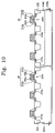
FIGS. 10 and 11 are simplified cross-sectional views for illustrating a method of fabricating a semiconductor device according to another embodiment of the present invention. Referring to FIG. 10, a device isolation layer 202 may be formed in a predetermined region of a semiconductor substrate of N-type and P- type regions 200 a and 200 b. A plurality of first active regions 204 a may be defined by an outline of the device isolation layer in N-type region 200 a. A plurality of second active regions 204 b may be defined by an outline of the device isolation layer in the P-type region 200 b. The N-type and P- type regions 200 a and 200 b may comprise N- and P-wells, respectively.
A gate insulation layer and a gate conductive layer may be formed on an entire surface of the resultant structure where the first and second active regions 204 a and 204 b have been defined by the outline of the device isolation layer. In certain embodiments, the gate insulation layer may comprise different thicknesses over respective N-type and P- type regions 200 a and 200 b. In addition, the gate conductive layers may comprise different conductivity types over respective N-type and P- type regions 200 a and 200 b.
Next, the gate conductive layer may be patterned to form first and second gate electrodes 208 a and 208 b that cross the first and second active regions 204 a and 204 b, respectively. A first gate insulation layer 206 a may be disposed between first gate electrodes 208 a and the surface of the first active regions 204 a, whereas a second gate insulation layer 206 b may be disposed between second gate electrodes 208 b and the surface of the second active regions 204 b.
The first gate electrodes 208 a may then be used as an ion implantation mask while implanting P-type impurities to form a P-type lightly diffused layer 210 a in the first active region 204 a on opposite sides of each first gate electrode 208 a. Similarly, N-type impurities may be implanted while using the second gate electrode 208 b as an ion implantation mask and forming N-type lightly diffused layer 210 b in the second active region 204 b at both sides of each second gate electrode 208 b. Thereafter, first sidewall spacers 212 a may be formed on sidewalls of each first gate electrode 208 a, and second sidewall spacers 212 b may be formed on sidewalls of each second gate electrode 208 b. The first gate electrode 208 a, the first gate insulation layer 206 a and the first sidewall spacer 212 a may be referenced collectively as a first gate pattern g3. Likewise, the second gate electrode 208 b, the second gate insulation layer 206 b and the second sidewall spacer 212 b may be referenced collectively as a second gate pattern g4.
Referring to FIG. 11, by using the first gate patterns g3 as an ion implantation mask, impurity ions may be implanted into exposed regions of first active regions 204 a to form a P-type heavily diffused layer 214 a. Likewise, impurity ions may be implanted into exposed regions of the second active regions 204 b while using the second gate patterns g4 as an ion implantation mask to form N-type heavily diffused layer 214 b. The P-type lightly diffused layer and the P-type heavily diffused layer together form P-type source/drain regions 216 a. Likewise, the N-type lightly diffused layer and the N-type heavily diffused layer together form N-type source/drain regions 216 b.
The first gate patterns g3 as well as the P-type source/drain regions 216 a disposed in the first active regions 204 a constitute PMOS transistors. While in the second active regions 204 b, the second gate patterns g4 as well as the N-type source/drain regions 216 b constitute NMOS transistors. The portions of device isolation layer 202 adjacent to one of the P-type source/drain regions 216 a of each PMOS transistor may be etched to form first recesses 220 a, whereas other portions of device isolation layer 202 adjacent to one of the N-type source/drain regions 216 b of each NMOS transistor may be etched to form second recesses 220 b. Portions of N-type region 200 a under the respective P-type source/drain regions 216 a neighboring the first recessed may be exposed by the first recesses 220 a, and portions of the P-type region 200 b under the N-type source/drain regions 216 b may be exposed by the second recesses 220 b.
Although not shown in the drawings of FIGS. 10–11, a silicidation process, as described earlier herein relative to FIGS. 7–8, may be used to form salicide layers (224 a, 224 b, 226 a, and 226 b of FIG. 9). According to this embodiment of the present invention, portions of the device isolation layer adjacent to each of a plurality of NMOS and PMOS transistors may be recessed so that a bias can be applied to exposed regions of a well or substrate within the recesses. As a result, an area requisite for well biasing may be reduced while, at the same time, it may assist prevention of the latch-up phenomenon.
According to particular exemplary embodiments described above, portions of the device isolation layer may be recessed to expose regions of a semiconductor substrate or well under each transistor. A common bias may then be applied to both the exposed regions of the semiconductor substrate or well and the respective source/drain regions of the transistors. Consequently, the common biasings proximate the respective transistors may be capable of preventing the latch-up phenomenon or noise and may be realized without need for an increase in the area of the semiconductor device as might otherwise be required to accommodate the well biasing provisions.
In the drawings and specification, there have been disclosed typical embodiments of this invention and, although specific terms are employed, they may be used in a generic and descriptive sense only and not for purposes of limitation. Additionally, it will be apparent to those skilled in this art that the particular embodiments illustrated or described herein are exemplary and that various changes and modifications may be made thereto as become apparent upon reading the present disclosure. Accordingly, such changes and modifications shall be deemed to fall within the scope of the appended claims.