US7054404B2 - Clock control method, frequency dividing circuit and PLL circuit - Google Patents
Clock control method, frequency dividing circuit and PLL circuit Download PDFInfo
- Publication number
- US7054404B2 US7054404B2 US10/225,361 US22536102A US7054404B2 US 7054404 B2 US7054404 B2 US 7054404B2 US 22536102 A US22536102 A US 22536102A US 7054404 B2 US7054404 B2 US 7054404B2
- Authority
- US
- United States
- Prior art keywords
- frequency
- interpolator
- circuit
- value
- output
- Prior art date
- Legal status (The legal status is an assumption and is not a legal conclusion. Google has not performed a legal analysis and makes no representation as to the accuracy of the status listed.)
- Expired - Fee Related, expires
Links
Images


Classifications
-
- H—ELECTRICITY
- H03—ELECTRONIC CIRCUITRY
- H03L—AUTOMATIC CONTROL, STARTING, SYNCHRONISATION OR STABILISATION OF GENERATORS OF ELECTRONIC OSCILLATIONS OR PULSES
- H03L7/00—Automatic control of frequency or phase; Synchronisation
- H03L7/06—Automatic control of frequency or phase; Synchronisation using a reference signal applied to a frequency- or phase-locked loop
- H03L7/16—Indirect frequency synthesis, i.e. generating a desired one of a number of predetermined frequencies using a frequency- or phase-locked loop
- H03L7/18—Indirect frequency synthesis, i.e. generating a desired one of a number of predetermined frequencies using a frequency- or phase-locked loop using a frequency divider or counter in the loop
- H03L7/197—Indirect frequency synthesis, i.e. generating a desired one of a number of predetermined frequencies using a frequency- or phase-locked loop using a frequency divider or counter in the loop a time difference being used for locking the loop, the counter counting between numbers which are variable in time or the frequency divider dividing by a factor variable in time, e.g. for obtaining fractional frequency division
- H03L7/1974—Indirect frequency synthesis, i.e. generating a desired one of a number of predetermined frequencies using a frequency- or phase-locked loop using a frequency divider or counter in the loop a time difference being used for locking the loop, the counter counting between numbers which are variable in time or the frequency divider dividing by a factor variable in time, e.g. for obtaining fractional frequency division for fractional frequency division
- H03L7/1976—Indirect frequency synthesis, i.e. generating a desired one of a number of predetermined frequencies using a frequency- or phase-locked loop using a frequency divider or counter in the loop a time difference being used for locking the loop, the counter counting between numbers which are variable in time or the frequency divider dividing by a factor variable in time, e.g. for obtaining fractional frequency division for fractional frequency division using a phase accumulator for controlling the counter or frequency divider
-
- G—PHYSICS
- G06—COMPUTING OR CALCULATING; COUNTING
- G06F—ELECTRIC DIGITAL DATA PROCESSING
- G06F7/00—Methods or arrangements for processing data by operating upon the order or content of the data handled
- G06F7/60—Methods or arrangements for performing computations using a digital non-denominational number representation, i.e. number representation without radix; Computing devices using combinations of denominational and non-denominational quantity representations, e.g. using difunction pulse trains, STEELE computers, phase computers
- G06F7/68—Methods or arrangements for performing computations using a digital non-denominational number representation, i.e. number representation without radix; Computing devices using combinations of denominational and non-denominational quantity representations, e.g. using difunction pulse trains, STEELE computers, phase computers using pulse rate multipliers or dividers pulse rate multipliers or dividers per se
-
- H—ELECTRICITY
- H03—ELECTRONIC CIRCUITRY
- H03L—AUTOMATIC CONTROL, STARTING, SYNCHRONISATION OR STABILISATION OF GENERATORS OF ELECTRONIC OSCILLATIONS OR PULSES
- H03L7/00—Automatic control of frequency or phase; Synchronisation
- H03L7/06—Automatic control of frequency or phase; Synchronisation using a reference signal applied to a frequency- or phase-locked loop
- H03L7/08—Details of the phase-locked loop
- H03L7/081—Details of the phase-locked loop provided with an additional controlled phase shifter
-
- H—ELECTRICITY
- H03—ELECTRONIC CIRCUITRY
- H03L—AUTOMATIC CONTROL, STARTING, SYNCHRONISATION OR STABILISATION OF GENERATORS OF ELECTRONIC OSCILLATIONS OR PULSES
- H03L7/00—Automatic control of frequency or phase; Synchronisation
- H03L7/06—Automatic control of frequency or phase; Synchronisation using a reference signal applied to a frequency- or phase-locked loop
- H03L7/16—Indirect frequency synthesis, i.e. generating a desired one of a number of predetermined frequencies using a frequency- or phase-locked loop
- H03L7/18—Indirect frequency synthesis, i.e. generating a desired one of a number of predetermined frequencies using a frequency- or phase-locked loop using a frequency divider or counter in the loop
- H03L7/197—Indirect frequency synthesis, i.e. generating a desired one of a number of predetermined frequencies using a frequency- or phase-locked loop using a frequency divider or counter in the loop a time difference being used for locking the loop, the counter counting between numbers which are variable in time or the frequency divider dividing by a factor variable in time, e.g. for obtaining fractional frequency division
- H03L7/1974—Indirect frequency synthesis, i.e. generating a desired one of a number of predetermined frequencies using a frequency- or phase-locked loop using a frequency divider or counter in the loop a time difference being used for locking the loop, the counter counting between numbers which are variable in time or the frequency divider dividing by a factor variable in time, e.g. for obtaining fractional frequency division for fractional frequency division
-
- H—ELECTRICITY
- H03—ELECTRONIC CIRCUITRY
- H03K—PULSE TECHNIQUE
- H03K5/00—Manipulating of pulses not covered by one of the other main groups of this subclass
- H03K2005/00013—Delay, i.e. output pulse is delayed after input pulse and pulse length of output pulse is dependent on pulse length of input pulse
- H03K2005/00019—Variable delay
- H03K2005/00058—Variable delay controlled by a digital setting
- H03K2005/00065—Variable delay controlled by a digital setting by current control, e.g. by parallel current control transistors
-
- H—ELECTRICITY
- H03—ELECTRONIC CIRCUITRY
- H03K—PULSE TECHNIQUE
- H03K5/00—Manipulating of pulses not covered by one of the other main groups of this subclass
- H03K2005/00013—Delay, i.e. output pulse is delayed after input pulse and pulse length of output pulse is dependent on pulse length of input pulse
- H03K2005/00019—Variable delay
- H03K2005/00058—Variable delay controlled by a digital setting
- H03K2005/00071—Variable delay controlled by a digital setting by adding capacitance as a load
-
- H—ELECTRICITY
- H03—ELECTRONIC CIRCUITRY
- H03L—AUTOMATIC CONTROL, STARTING, SYNCHRONISATION OR STABILISATION OF GENERATORS OF ELECTRONIC OSCILLATIONS OR PULSES
- H03L7/00—Automatic control of frequency or phase; Synchronisation
- H03L7/06—Automatic control of frequency or phase; Synchronisation using a reference signal applied to a frequency- or phase-locked loop
- H03L7/08—Details of the phase-locked loop
- H03L7/085—Details of the phase-locked loop concerning mainly the frequency- or phase-detection arrangement including the filtering or amplification of its output signal
- H03L7/089—Details of the phase-locked loop concerning mainly the frequency- or phase-detection arrangement including the filtering or amplification of its output signal the phase or frequency detector generating up-down pulses
- H03L7/0891—Details of the phase-locked loop concerning mainly the frequency- or phase-detection arrangement including the filtering or amplification of its output signal the phase or frequency detector generating up-down pulses the up-down pulses controlling source and sink current generators, e.g. a charge pump
Definitions
- This invention relates to a frequency dividing circuit and to a phase-locked loop (PLL) equipped with the frequency dividing circuit. More particularly, the invention relates to a variable frequency dividing circuit that employs an interpolator, and to a PLL having this frequency dividing circuit.
- PLL phase-locked loop
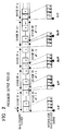
- FIG. 14 is a diagram illustrating the structure of a conventional PLL equipped with a variable frequency divider has pulse-swallow architecture.
- the PLL comprises an amplifier 201 for amplifying the output (whose frequency ftcxo is 14.4 MHz) of an externally mounted temperature-compensated crystal oscillator (TCXO) 200 ; a reference-frequency dividing circuit 202 for frequency-dividing the output of the amplifier 201 ; a phase comparator 203 for sensing the phase difference between a reference signal (frequency f ⁇ 400 KHz), which is the result of frequency division by the reference-frequency dividing circuit 202 , and a frequency-divided clock; a charge pump 204 for charging a capacitance (not shown) when the phase comparator 203 is outputting an UP signal in accordance with the result of the phase comparison and for discharging the charge, which has accumulated in the capacitance, when the phase comparator 203 is outputting a DOWN signal in accordance with the result of the phase comparison; a low-pass filter (loop filter) LPF 205 for smoothing the terminal voltage of the capacitance charged/discharged
- An MC (modulus control) signal supplied to the prescaler 207 from the B counter 210 is a control signal for changing the frequency-dividing factor of the P, (P+1) frequency dividing prescaler 207 .
- the prescaler 207 functions as a divide-by-P prescaler when the signal MC is at HIGH level and as a divide-by-(P+1) prescaler when the signal MC is at LOW level.
- FIG. 15 is a diagram illustrating the prescaler 207 and counters 209 and 210 extracted from the PLL circuit shown in FIG. 14 .
- the prescaler 207 includes D-type flip-flops 22 to 25 each of which has its data output terminal connected to the data input terminal of the D-type flip-flop of the next stage and each of which has a clock terminal to which an output signal of the voltage-controlled oscillator (referred to simply as a “VCO”) 206 is supplied to thereby construct a 4-stage shift register; an OR gate 21 having a first input terminal connected to an inverting output terminal QB of the D-type flip-flop 25 and an output terminal connected to the data input terminal of the D-type flip-flop 22 ; an OR gate 26 having a non-inverting output terminal Q of the D-type flip-flop 25 and the output terminal of an OR gate 28 connected to first and second input terminals, respectively; and a D-type flip-flop 27 having the output terminal of the OR gate 26 connected to its data input terminal and having the output clock of the VCO 206 input to its clock terminal.
- VCO voltage-controlled oscillator
- the D-type flip-flop 27 has an inverting output terminal QB connected to the second input terminal of the OR gate 21 .
- the non-inverting output terminal Q of the D-type flip-flop 25 is input to the clock input terminal of the D-type flip-flop 29 and the inverting output terminal QB of the D-type flip-flop 29 is connected to its own data input terminal to thereby construct a frequency dividing circuit.
- the non-inverting output terminal Q of the D-type flip-flop 29 is input to the clock input terminal of the D-type flip-flop 30 and the inverting output terminal QB of the D-type flip-flop 30 is connected to its own data input terminal to thereby construct a frequency dividing circuit.
- the non-inverting output terminal Q of the D-type flip-flop 30 is output to the A counter 209 and B counter 210 as the frequency-divided output of the prescaler 207 .
- the MC signal and the non-inverting output terminals Q of the D-type flip-flops 29 and 30 are input to the OR gate 28 , the output of which is input to the OR gate 26 .
- the prescaler 207 is of the type that performs frequency division by 32 or 33 .
- the 4-stage shift register comprising the D-type flip-flops 22 , 23 , 24 , and 25 is driven by the output clock of the VCO 206 to perform frequency division by 8.
- the 4-stage shift register comprising the D-type flip-flops 22 , 23 , 24 , and 25 composes a 4-bit ring counter driven by the output clock of the VCO 206 . If the inverting output terminal QB of the D-type flip-flop 25 is “1”, the output of the OR gate 21 is “1”. One round is completed by eight clocks, which enter one at a time as the output clock from the VCO 206 .
- the states of the D-type flip-flops 25 , 24 , 23 , and 22 undergo a transition as follows: The state initially is “0000” and becomes “0001”, “0011”, “0111”“1111”, “1110”, “1100”, “1000”, and “0000” at the first, second, third, fourth, fifth, sixth, seventh and eighth clocks, respectively, of the output clocks from the VCO 206 .
- the D-type flip-flop 25 alternatingly outputs four clocks of successive “1”s and four clocks of successive “0”s.
- the output of the D-type flip-flop 25 is a signal obtained by 1/8 division of the frequency of the output clock from the VCO 206 .
- the output of the D-type flip-flop 25 is input to the OR gate 26 .
- the OR gate 26 inputs “1” to the data input terminal of the D-type flip-flop 27 and the inverting output terminal QB of the D-type flip-flop 27 is made “0”.
- the non-inverting output terminals Q of the D-type flip-flops 29 and 30 enter the OR gate 28 , the output of which is input to the data input terminal of the D-type flip-flop 27 via the OR gate 26 .
- the two stages of D-type flip-flops 29 and 30 compose a divide-by-4 frequency dividing circuit.
- the output of the 4-stage shift register comprising the D-type flip-flops 22 , 23 , 24 and 25 is divided by 4 by the D-type flip-flops 29 and 30 .
- division by 32 is achieved.
- the OR gate 26 transmits the output at the non-inverting output terminal Q of D-type flip-flop 25 to the data input terminal D of the D-type flip-flop 27 .
- the flip-flops 29 and 30 clocked by the 1/8 frequency-divided output of the 4-stage register comprising the D-type flip-flops 22 , 23 , 24 and 25 changes in state in the manner “1010”, and “1100”.
- the output of the OR gate 28 becomes “0” if the outputs of the flip-flops 29 , 30 both become “0”, i.e., at a rate of once per four clocks output from the D-type flip-flop 25 .
- the D-type flip-flop 27 constructs a shift register together with the D-type flip-flops 22 , 23 , 24 , and 25 .
- the OR gate 26 transmits the output of the D-type flip-flop 25 to the data input terminal of the D-type flip-flop 27 as is.
- the states of the D-type flip-flops 27 , 25 , 24 , 23 , and 22 undergo a transition in nine clock cycles in the following manner: “10000”, “00001”, “00011”, “00111”, “01111”, “11111”, “11110”, “11100”, “11000”, and “10000”.
- the shift register of prescaler 207 implements frequency division by 9. Among the four cycles of the divide-by-4 frequency dividing circuit of D-type flip-flops 29 and 30 , division by 8 are executed in three cycles and division by 9 in one cycle.
- N is obtained by frequency division by 32, 33
- a pulse-swallow counter is implemented by the combination of two binary counters 209 and 210 .
- a is the quotient obtained by dividing N by 32, e.g., a value of the six higher order bits or more, and b takes on the value of the five lower order bits.
- the A counter 209 and B counter 210 both count up to set count values A′, B′ or count down from the set values A′, B′ simultaneously in response to the output of the prescaler 207 .
- the values A′, B′ become a, b, respectively.
- the MC signal is placed at LOW level and the prescaler 207 performs division by 33.
- the B counter 210 counts the 1/33 frequency-divided output of the prescaler 207 b times.
- the MC signal is placed at HIGH level.
- the A counter 209 counts the 1/32 frequency-divided output of the prescaler 207 (a ⁇ b) times, namely the remaining number of times until the count value a is attained or until 0 is reached starting from a.
- the MC signal supplied to the prescaler 207 is required to operate earlier than the output period of the prescaler 207 , which performs a high-speed frequency dividing operation. This makes it difficult to design the proper timing.
- variable frequency divider relying upon the pulse-swallow counter arrangement is used to achieve frequency division to the desired frequency in a variable frequency dividing circuit for adjusting the frequency multiplication factor of a synthesizer PLL, etc.
- frequency division in the high-speed portion is carried out by a dual modulus prescaler having two frequency-dividing factors P and P+1 [1/P, 1/(P+1) frequency division]
- P and P+1 the frequency-dividing factors
- a large amount of power is consumed owing to the parallel arrangement of the A counter and B counter constituting the programmable counters.
- the timing of the MC (modulus control) signal which is the signal that controls the changeover of the number of frequency divisions of the dual modulus prescaler. As a consequence, high-speed operation is difficult.
- the prescaler, counter and control circuit, etc. are placed close together taking into consideration wiring delay of the MC signal, which requires high-speed operation. This makes it difficult to place the prescaler and control circuit on separate chips, thereby limiting freedom of circuit design.
- variable frequency dividing circuit that reduces power consumption and facilitates design of timing
- PLL circuit equipped with this frequency dividing circuit
- method of clock control a variable frequency dividing circuit that reduces power consumption and facilitates design of timing
- variable frequency dividing circuit in accordance with one aspect of the present invention, which comprises a first frequency dividing circuit for performing frequency-division of an input signal by a first value P (where P is a positive integer); a second frequency dividing circuit for dividing the P-frequency-divided output of the first frequency dividing circuit by a second value A (where A is a positive integer); a circuit for generating two signals, which have a phase difference equivalent to one period of the P-frequency-divided output of the first frequency dividing circuit, whenever frequency-division by A is performed by the second frequency dividing circuit; and an interpolator, to which the two generated signals are input, for generating and outputting an output signal of a phase obtained by interpolating the phase difference between the two input signals in accordance with an interior division ratio set by a control signal applied thereto; wherein the interpolator produces an output signal, the phase of which is a predetermined multiple of a unit obtained by dividing the phase difference equivalent to one
- a variable frequency dividing circuit comprising a first frequency dividing circuit for performing frequency-division of an input signal by a first value P (where P is a positive integer); a second frequency dividing circuit for dividing the P-frequency-divided output of the first frequency dividing circuit by a second value A (where A is a positive integer); a circuit for generating two signals, which have a phase difference equivalent to one period of the P-frequency-divided output of the first frequency dividing circuit, whenever frequency-division by A is performed by the second frequency dividing circuit; an interpolator, to which the two generated signals are input, for generating and outputting an output signal of a phase obtained by interpolating the phase difference between the two signals in accordance with an interior division ratio set by a control signal applied thereto; the interpolator adopting P ⁇ M (where M is a predetermined positive integer) as the dividing number of the phase difference; and the interpolator producing an output signal
- a PLL circuit in accordance with a further aspect of the present invention comprises a phase comparator circuit having a first input terminal to which a reference clock is applied for outputting a phase difference; a charge pump for generating a voltage conforming to the phase difference output from the phase comparator circuit; a loop filter for smoothing the voltage conforming to the phase difference; a voltage-controlled oscillator, to which an output of the loop filter is input as a control signal, for outputting a clock having an oscillation frequency prescribed by the control signal; a first frequency dividing circuit, to which the output clock of the voltage-controlled oscillator is input, for performing frequency-division of the clock signal by a first value P; a second frequency dividing circuit for dividing the P-frequency-divided output of the first frequency dividing circuit by a second value A; a circuit for generating two signals, which have a phase difference equivalent to one period of the P-frequency-divided output of the first frequency dividing circuit, whenever frequency-division by A is performed by the second frequency
- the interpolator adopts P ⁇ M (where M is a predetermined positive integer) as the dividing number of the phase difference, and produces an output signal, the phase of which is a predetermined multiple of a unit obtained by dividing the phase difference equivalent to one period of the P-frequency-divided output of the first frequency dividing circuit by P ⁇ M; and a control circuit is provided for exercising control in such a manner that a fixed value B ⁇ M+K (where K is a predetermined positive integer than is less than M) is added to a preceding value C 1 of an interior division ratio C 1 :P ⁇ C 1 of the interpolator whenever frequency-division by A is performed by the second frequency dividing circuit, a remainder obtained by dividing the result of addition by P ⁇ M is adopted as the present value C 1 of the interior division ratio of the interpolator, and if the value obtained by adding the constant value B ⁇ M+K to the preceding value C 1 of the interior division ratio is equal to or greater than
- a clock control method in accordance with a further aspect of the present invention comprises the steps of performing frequency-division of an input signal by P (where P is a positive integer) by a first frequency dividing circuit; dividing the P-frequency-divided output of the first frequency dividing circuit by value A (where A is a positive integer) by a second frequency dividing circuit; generating two signals, which have a phase difference equivalent to one period of the P-frequency-divided output of the first frequency dividing circuit, whenever frequency-division by A is performed by the second frequency dividing circuit; inputting the two signals to an interpolator and generating and outputting an output signal having a phase obtained by interpolating the phase difference between the two signals in steps of B/P (where B is a positive integer less than P) in accordance with an interior division ratio set by a control signal; and incrementing or decrementing the interior division ratio of the interpolator B/P at a time whenever division by A is performed; the frequency of the input signal being divided by A ⁇ P+B.
- This clock control method further includes steps of adding B, which decides C 1 of an interior division ratio C 1 :P ⁇ C 1 of the interpolator, to the preceding value of C 1 of the interior division ratio whenever frequency-division by A is performed by the second frequency dividing circuit, and calculating a remainder obtained by dividing the result of addition by P; setting the remainder to the value C 1 of the interior division ratio of the interpolator; and performing control to add 1 to the frequency dividing factor A of the second frequency dividing circuit when the result of adding B to the preceding value C 1 of the interior division ratio is equal to or greater than P, thereby performing division by A+1.
- FIG. 1 is a block diagram illustrating the basic structure of a first embodiment according to the present invention
- FIG. 2 is a diagram useful in describing the operation of the first embodiment
- FIG. 3 is a block diagram illustrating the structure of a first embodiment according to the present invention.
- FIG. 4 is a block diagram illustrating the structure of a second embodiment according to the present invention.
- FIG. 5 is a diagram illustrating the structure of an interpolator used in the embodiments of the present invention.
- FIG. 6 is a diagram illustrating the structure of an interpolator used in the embodiments of the present invention.
- FIG. 7 is a diagram illustrating the structure of an interpolator used in the embodiments of the present invention.
- FIG. 8 is a block diagram illustrating the structure of the first embodiment
- FIG. 9 is a diagram useful in describing the timing operation of the first embodiment
- FIG. 10 is diagram useful in describing the operation of the control circuit according to the first embodiment
- FIG. 11 is diagram useful in describing the operation of the control circuit according to the second embodiment.
- FIG. 12 is diagram useful in describing the operation of the control circuit according to a third embodiment of the present invention.
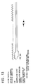
- FIG. 13 is a diagram useful in describing an operation for controlling the interpolator according to the embodiments.
- FIG. 14 is a diagram illustrating the structure of a PLL circuit having a pulse-swallow variable frequency dividing circuit.
- FIG. 15 is a diagram illustrating the structure of a prescaler shown in FIG. 14 .
- a frequency dividing circuit in accordance with a preferred embodiment of the present invention includes a first frequency dividing circuit ( 107 ) for performing frequency-division of an input signal by P (where P is a positive integer); a second frequency dividing circuit ( 109 ) for performing frequency-division of an output signal of the first frequency dividing circuit ( 107 ) by A (where A is a positive integer); a circuit ( 121 , 122 , 130 ) for generating two signals, which have a phase difference equivalent to one period of the P-frequency-divided output of the first frequency dividing circuit ( 107 ), whenever frequency-division by A is performed by the second frequency dividing circuit ( 109 ); an interpolator ( 123 ), which receives the two generated signals, for generating and outputting an output signal of a phase obtained by interpolating the phase difference between the two signals in steps of B/P (where B is a positive integer less than P)
- An arithmetic circuit ( 110 ) is provided for adding B to the preceding value C 1 of the interior division ratio (C 1 :P ⁇ C 1 ) of the interpolator ( 123 ) whenever frequency-division by A is performed by the second frequency dividing circuit ( 109 ), and outputting a remainder obtained by dividing the result of addition by P.
- a control circuit ( 130 ) is provided for performing control to set the remainder, which is output from the arithmetic circuit ( 110 ), to the value C 1 of the interior division ratio of the interpolator ( 123 ), and to add 1 to the frequency dividing factor A of the second frequency dividing circuit ( 109 ) when the result of adding B to the preceding value C 1 of the interior division ratio is equal to or greater than P, thereby performing division by A+1.
- the interpolator ( 123 ) is such that P ⁇ M (where M is a predetermined positive integer) represents the dividing number by which the phase difference is divided, and the interpolator ( 123 ) produces an output signal having a phase which is a prescribed multiple of a unit obtained by dividing the phase difference equivalent to one period of the P-frequency-divided output of the first frequency dividing circuit ( 107 ) by P ⁇ M.
- a control circuit ( 130 ) is provided for exercising control in such a manner that a fixed value B ⁇ M+K (where K is a predetermined positive integer that is less than M) is added to a preceding value C 1 of an interior division ratio C 1 :P ⁇ C 1 of the interpolator whenever frequency-division by A is performed by the second frequency dividing circuit ( 109 ), a remainder obtained by dividing the result of addition by P ⁇ M is adopted as the present value C 1 of the interior division ratio of the interpolator, and 1 is added to the frequency-dividing factor of the second frequency dividing circuit ( 109 ) to perform frequency-division by A+1 if the value obtained by adding the constant value B ⁇ M+K to the preceding value C 1 of the interior division ratio of the interpolator ( 123 ) is equal to or greater than P ⁇ M.
- the interpolator ( 123 ) produces an output signal in which the frequency of the input signal has been divided by a frequency-dividing factor that is equal to A ⁇ P+B+K/M.
- the interpolator has a two-stage architecture, as shown in FIG. 4 .
- a phase difference equivalent to one period of the P-frequency-divided output is interpolated by a first interpolator ( 123 ) in accordance with an interior division ratio C:P ⁇ C and by a second interpolator ( 124 ) in accordance with an interior division ratio C:P ⁇ (C+1).
- the phase difference 1/P (one period of the input signal) between the two signals output from the first and second interpolators ( 123 , 124 ) is interpolated by a third interpolator ( 125 ) in accordance with an interior division ratio C 2 :M ⁇ C 2 , whereby fractional division (A ⁇ P+B+K/M) is realized.
- the interior division ratio is incremented (or decremented) in steps of B whenever division by A is performed.
- the third interpolator ( 125 ) the interior division ratio is incremented (or decremented) in steps of K whenever division by A is performed.
- the first interpolator ( 123 ) interpolates phase in accordance with an interior division ratio C 2 :P ⁇ C 2 in steps of a value obtained by dividing the phase difference between the two input signals by P.
- the second interpolator ( 124 ) interpolates phase in accordance with an interior division ratio C 2 +1:P ⁇ (C 2 +1) in steps of a value obtained by dividing the phase difference between the two input signals by P.
- the third interpolator ( 125 ) interpolates phase in accordance with an interior division ratio C 3 :M ⁇ C 3 in steps of a value obtained by dividing the phase difference between the signals, which are output from the first and second interpolators ( 123 , 124 ), by M (where M is a predetermined positive integer).
- a control circuit ( 130 A) is provided for exercising control so as to make the total interior division ratio of the first to third interpolators equal to C 1 :P ⁇ M ⁇ C 1 , add a constant value B ⁇ M+K (where K is a predetermined positive integer that is less than M) to the preceding value C 1 of the total interior division ratio C 1 :P ⁇ C 1 , adopt a remainder, which is obtained by dividing the result of addition by P ⁇ M, as the present value C 1 of the total interior division ratio, and add 1 to the frequency-dividing factor of the second frequency dividing circuit ( 109 ) to perform frequency-division by A+1 if the value obtained by adding the constant value B ⁇ M+K to the preceding value C 1 of the total interior division ratio is equal to or greater than P ⁇ M.
- the value C 2 of the interior division ratios of the first and second interpolators ( 123 , 124 ) is an integral part obtained by dividing C 1 by M
- C 3 in the third interpolator ( 125 ) is the remainder obtained by dividing C 1 by M.
- the third interpolator ( 125 ) outputs a signal in which the frequency of the input signal has been divided by a frequency-dividing factor A ⁇ P+B+K/M.
- first and second interpolators ( 123 , 124 ) of a first stage, to which two signals are input, each for generating and outputting an output signal of a phase obtained by interpolating the phase difference between the two input signals in accordance with respective ones of interior division ratios set by a control signal applied thereto; and a third interpolator ( 125 ) of a successive stage, to which the outputs from the first and second interpolators ( 123 , 124 ) are input, for generating and outputting an output signal of a phase obtained by interpolating the phase difference between these two input signals.
- the first interpolator ( 123 ) interpolates phase in accordance with an interior division ratio C 5 :P ⁇ C 5 in steps of a value obtained by dividing the phase difference between the two input signals by P.
- the second interpolator ( 124 ) interpolates phase in accordance with an interior division ratio C 5 +1:P ⁇ (C 5 +1) in steps of a value obtained by dividing the phase difference between the two input signals by P.
- the third interpolator ( 125 ) interpolates phase in accordance with an interior division ratio C 4 :M ⁇ C 4 in steps of a value obtained by dividing the phase difference between the two inputs signals by M (where M is a predetermined positive integer).
- a control circuit ( 130 B) having first-stage control means for exercising control so as to add a third value B (where B is a predetermined positive integer that is less than P) to preceding values C 5 , C 5 +1 of the interior division ratios of the first and second interpolators ( 123 , 124 ) whenever frequency-division by A is performed by the second frequency dividing circuit ( 109 ), and adopt the remainders, which are obtained by dividing the results of addition by P, as the present values C 5 , C 5 +1 of the first and second interpolators, respectively; and second-stage control means for exercising control so as to add a fourth value K (where K is a predetermined positive integer that is less than M) to the preceding value C 4 of the interior division ratio of the third interpolator ( 125 ) whenever frequency-division by A is performed by the second frequency dividing circuit ( 109 ), and adopt the remainder, which is obtained by dividing the result of addition by M, as the present value C 4 of the third interpolator (
- the control circuit ( 130 B) adds 1 to B if the value obtained by adding K to the preceding value C 4 of the interior division ratio of the third interpolator ( 125 ) is equal to or greater than M, and adds 1 to the frequency dividing factor A of the second frequency dividing circuit if the value obtained by adding B to the preceding value C 5 of the first and second interpolators ( 123 , 124 ) is equal to or greater than P.
- the third interpolator produces an output signal in which the frequency of the input signal has been divided by a frequency-dividing factor A ⁇ P+B+K/M.
- a PLL circuit comprises a phase comparator circuit ( 103 ) to which a reference signal is input; a charge pump ( 104 ) for generating a voltage corresponding to a phase difference by charging or discharging a capacitance based upon a signal output from the phase comparator circuit ( 103 ); a loop filter ( 105 ) for smoothing the voltage corresponding to the phase difference; and a voltage-controlled oscillator ( 106 ), to which the output voltage of the loop filter ( 105 ) is input as a control voltage, for outputting a clock having an oscillation frequency that corresponds to the control voltage; wherein the output clock of the voltage-controlled oscillator ( 106 ) is frequency-divided by a frequency dividing circuit and fed back to the phase comparator circuit ( 103 ).
- the frequency dividing circuit of the PLL circuit in which the phase difference between a reference clock and a frequency-divided clock is sensed by the phase comparator circuit ( 103 ), is constituted by the variable
- a first frequency dividing circuit ( 107 ) to which a clock having the oscillation frequency of a voltage-controlled oscillator ( 106 ) is input, for performing frequency-division of the clock at high speed is obtained by cascade-connecting simple toggle circuits (a frequency dividing circuit based upon D-type flip-flops).
- the PLL circuit outputs a signal having a phase obtained by interpolating a phase difference equivalent to one period of the frequency-divided output of the first frequency dividing circuit in accordance with an applied division ratio, thereby implementing integral frequency division (A ⁇ P+B) or fractional frequency division (A ⁇ P+B+K/M).
- a second frequency dividing circuit is provided for dividing the P-frequency-divided output of the first frequency dividing circuit by A. Two counters, which are required in a pulse-swallow variable frequency dividing circuit, at no longer necessary.
- a prescaler and a phase adjusting circuit are provided, the number of high-speed operating elements is reduced and, hence, so is power consumption, in comparison with an arrangement having a P/P+1 prescaler.
- the prescaler is simple in construction and is ideal for high-speed operation. Further, in comparison with the pulse-swallow arrangement, the present invention is such that only one counter suffices as a programmable counter and less power is consumed. Furthermore, the interpolator and control circuit operate only one time in an interval in which the P-frequency-divided output of the prescaler is divided by A, as a result of which power consumption is reduced.
- control is simplified because there is no longer need for a modulus control signal for changing the frequency-dividing factor of a P/P+1 prescaler.
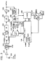
- FIG. 1 is a block diagram illustrating the structure of a PLL having a variable frequency dividing circuit according to the present invention.
- TCXO temperature-compensated
- a phase adjusting circuit 120 adjusts the phase of the P-frequency-divided output of the frequency dividing circuit 107 whenever frequency-division by A is performed by the A counter 109 .
- the phase adjusting circuit 120 includes a D-type flip-flop 121 having a data input terminal to which a timing control signal from the control circuit 130 is applied and a clock input terminal to which the output of the frequency dividing circuit 107 is applied; a D-type flip-flop 122 having a data input terminal to which the output signal of the D-type flip-flop 121 is applied and a clock input terminal to which the output of the frequency dividing circuit 107 is applied; and an interpolator 123 having first and second input terminals to which the outputs of the D-type flip-flops 121 , 122 , respectively, are applied, for producing an output signal corresponding to a phase obtained by internally dividing the phase difference between the signals, which are applied to the first and second input terminals, based upon a control signal C from the control circuit 130 .
- the output of the interpolator 123 is input to the phase comparator 103 .
- the reference-frequency dividing circuit 102 is assumed to have a frequency-dividing factor R of 36, for example, and outputs a reference signal having a frequency (reference frequency) fr that is equal to 400 kHz.
- the output frequency of the VCO 106 is of the 800 MHz band 680.4 to 766.4 MHz) or 1.5 GHz band (1143.2 to 1370.95 MHz), by way of example.
- This embodiment of the present invention is equipped with the frequency dividing circuit (prescaler) 107 , which performs high-speed frequency division, and the interpolator 123 , which performs an interior division of the phase difference between its two input signals to vary the phase of the output signal, as a variable frequency dividing circuit for adjusting the frequency multiplication factor of a synthesizer PLL or the like, and outputs a signal obtained by interpolating the phase difference equivalent to the period of the P-frequency-divided output of the frequency dividing circuit 107 , thereby fractionally dividing the P-frequency-divided output of the frequency dividing circuit 107 to implement a programmable frequency divider (variable frequency divider).
- a programmable frequency divider variable frequency divider
- the frequency-dividing factor of the frequency dividing circuit 107 is P, and there is no switching between division by P and division by P+1. Accordingly, a register obtained by cascade-connecting flip-flops constitutes the frequency dividing circuit 107 . Further, in this embodiment of the present invention, a B counter ( 210 in FIGS. 14 and 15 ), which is required in a pulse-swallow variable frequency divider, is not provided.
- the interpolator 123 is set to a ratio C 1 :P ⁇ C 1 , which is for internally dividing the phase difference between the two signals input thereto, by the control signal C, and is implemented by an interpolator of the type which inhibits feedthrough current, as will be described later.
- the output frequency fvco of the VCO 106 is divided down to fvco/P by the frequency dividing circuit 107 , then this is further divided by A in the A counter 109 to obtain (fvco/P)/A
- the remainder calculating unit 110 Whenever the remainder calculating unit 110 receives a signal output from the A counter 109 , which occurs each time the divided-by-P output of the frequency dividing circuit 107 is counted A times, i.e., whenever division by A is performed, the remainder calculating unit 110 adds B successively, calculates the remainder obtained by dividing the sum by P and supplies the control circuit 130 with the remainder as a value for setting the interior division ratio of the interpolator 123 .
- the remainder calculating unit 110 adds B whenever frequency-division by A is performed by the A counter 109 and outputs, to the control circuit 130 , the remainder MOD (nB,P), in which P of nB, which is the result of addition, is the modulus.
- the calculation symbol MOD (p,q) represents a remainder r obtained by dividing p by q.
- the control circuit 130 outputs the control signal C, which controls the interior division ratio of interpolation by the interpolator 123 , based upon the signal output from the A counter 109 whenever it divides by A (this signal is output at such time that the A counter 109 counts down to a value of zero or at such time that the A counter 109 counts up to the value A) and the output signal MOD (nB,P) from the remainder calculating unit 110 .
- the interpolator 123 On the basis of the control signal C, the interpolator 123 outputs a signal having a phase obtained by performing an interior division of the phase difference between the two input signals at a ratio C:P ⁇ C.
- control circuit 130 supplies the data input terminal of the D-type flip-flop 121 of phase adjusting circuit 120 with a HIGH-level timing control signal (Timing Control) whenever frequency-division by A is performed by the A counter 109 .
- the D-type flip-flop 121 to the clock input terminal of which the P-frequency-divided output signal of the frequency dividing circuit 107 is applied, latches the timing control signal, which is output from the control circuit 130 whenever frequency-division by A is performed by the A counter 109 , at the rising edge of the P-frequency-divided output signal from the frequency dividing circuit 107 .
- the second CMOS transfer gate 122 latches and outputs the output signal of the D-type flip-flop 121 at a rising edge of the next P-frequency-divided output signal from the frequency dividing circuit 107 .
- the output signals of the D-type flip-flops 121 and 122 are fed to the interpolator 123 .
- the phase difference with regard to the rising edges of the output signals from the D-type flip-flops, 121 and 122 coincides with one period of the P-frequency-divided output of frequency dividing circuit 107 .
- the interpolator 123 produces an output signal having a phase obtained by incrementing or decrementing the preceding phase by B/P in steps of a value obtained by dividing one period of the P-frequency-divided output of the frequency dividing circuit 107 by P whenever division by A is performed, namely at the period at which interpolator 123 performs interpolation.
- the period 1/fvco of the oscillating clock of VCO 106 be one unit.
- the currently interpolated phase of the (i+1)th output signal of interpolator 123 lags the previously interpolated phase of the i-th signal by B/P in steps of a value obtained by dividing one period of the P-frequency-divided output of frequency dividing circuit 107 by P.
- the frequency-dividing factor N is equal to A ⁇ P+B.
- a phase difference equivalent to the period fvco/P of the frequency dividing circuit 107 is interpolated by the interpolator 123 in steps of resolution 1/P, and use is made of a timing obtained by adding or subtracting a fixed ratio (B/P) at a time whenever frequency-division by A is performed by the A counter 109 , thereby making it possible to divide by AP+B.
- Any frequency-dividing factor N equivalent to that in an arrangement that relies upon a modulus control prescaler, is realized, and any frequency multiplication factor is implemented.
- the output of the frequency dividing circuit 107 is subjected to a correction, which adds on the phase of the interior division ratio b/P, by the interpolator 123 whenever division by a is performed.
- the main frequency divider shown in FIG. 2 refers to a frequency divider that is a combination of the frequency dividing circuit 107 and phase adjusting circuit 120 of FIG. 1 .
- the main frequency divider implements division by a ⁇ P+b.
- interpolation of the phase of the output signal in interpolator 123 is updated in the manner 0/P, b/P, 2b/P, 3b/P, . . . , whenever frequency-division by a is performed, in steps of 1/P of one period of the P-frequency-divided output of the frequency dividing circuit 107 .
- interpolation of phase by the interpolator 123 involves incrementing in the manner 0/P, b/P, 2b/P, 3b/P, . . . , whenever division by a is performed, in steps of 1/P of one period of the P-frequency-divided output of the frequency dividing circuit 107 .
- decrementing is performed in the manner P/P, (P ⁇ b)/P, (P ⁇ 2b)/P, (P ⁇ 3b)/P, . . . (P ⁇ nb)/P, . . . , whenever frequency-division by a is performed.
- the difference between the currently interpolated phase of the output signal of interpolator 123 and the previously interpolated phase of the output signal is b/P and the interpolator 123 outputs a signal of period a ⁇ P+b in steps of the period 1/fvco) of the output clock of VCO 106 .
- the phase dividing ratio is made [P ⁇ MOD(nb,P)]/P.
- the first embodiment shown in FIG. 1 is such that the frequency dividing circuit (prescaler) 107 , which divides the output clock of the VCO 106 at high speed, is constituted by ECL (emitter-coupled logic), and an ECL/CMOS interface 108 is provided for converting between an ECL level and a CMOS level.
- An arithmetic unit constitutes the remainder calculating circuit 110 in FIG. 1 111 and latch 112 .
- the arithmetic unit 111 adds the constant B, which divides the interior division ratio of the interpolator 123 , to the present value being held in the latch 112 . If the sum becomes greater than P, the arithmetic unit 111 performs subtraction by P and outputs the value to the latch 112 .
- the control circuit 130 On the basis of the output of A counter 109 , the control circuit 130 outputs the timing control signal whenever division by A is performed, namely the period at which interpolator 123 performs interpolation. In addition, the control circuit 130 decodes the remainder MOD (nB,P) from the remainder calculating unit 110 and outputs the control signal C (a binary parallel signal) so that the interpolator 123 performs interpolation at an interior division ratio corresponding to MOD (nB,P)/P.
- gate control is performed so as to activate a gate circuit and transmit the P-frequency-divided output for a predetermined period of time starting from a timing decided whenever the A counter A counter 109 divides by A. At times other than this period of time, supply of the P-frequency-divided clock from the ECL/CMOS circuit 108 is disabled to thereby control power consumption.
- FIG. 4 is a block diagram illustrating the structure of a second embodiment according to the present invention.
- the interpolator 123 is such that phase division changes by B/P at a time in steps of 1/P of one period of the P-frequency-divided output, based upon a control signal C 2 , whenever frequency-division by A is performed by the A counter 109 .
- the interpolator 124 is such that phase division changes by B/P at a time in steps of 1/P of one period of the P-frequency-divided output, based upon a control signal C 2 , whenever frequency-division by A is performed by the A counter 109 .
- the interior division ratio is (B+1)/P, which is a value larger than that of the interpolator 123 by one step.
- the phase difference between the output signals of the interpolators 123 , and 124 is 1/P taking the divide-by-P period as a reference.
- the interpolator 125 outputs a signal whose phase is interpolated in steps obtained by further dividing the phase difference 1/P (equivalent to one period of the oscillating clock of VCO 106 ) between the outputs of interpolators 123 , and 124 by M.
- the interpolator 125 adds K to C 3 of the interior division ratio C 3 :M ⁇ C 3 whenever interpolation is performed and sets the interior division ratio by the remainder obtained by dividing the sum by M.
- the arithmetic unit (ALU) 111 and latch 112 calculate MOD (nB,P) whenever division by A is performed. More specifically, the arithmetic unit 111 adds B to the present value C 2 held in the latch 112 each time division by A is performed. When the sum exceeds P, the arithmetic unit 111 outputs a value, which is obtained by subtracting P from the sum, to the latch 112 as the remainder MOD (nB,P).
- An arithmetic unit (ALU) 113 and a latch 114 calculate MOD (nK,M).
- the arithmetic unit 113 adds K to the present value C 3 held in the latch 114 each time division by A is performed.
- the arithmetic unit 113 outputs a value, which is obtained by subtracting M from the sum, to the latch 113 as the remainder MOD (nK,M).
- the control circuit On the basis of the output of A counter 109 , the control circuit, here designated by 130 A, outputs the timing control signal whenever division by AP is performed, namely at the period at which interpolator 123 performs interpolation.
- the control circuit 130 A decodes MOD (nB,P) and outputs the control signal C 2 so that the output phases of the interpolators 123 and 124 are incremented by B/P, (B+1)/P, respectively, with the period of division-by-P serving as the reference.
- the interior division ratios for interpolating phase difference in the interpolators 123 , and 124 become C 2 :P ⁇ C 2 , and C 2 +1:P ⁇ (C 2 +1), respectively.
- the control circuit 130 A decodes MOD (nK,M) and outputs a control signal C in order to increment the output phase of interpolator 125 by K/M.
- the interior division ratio for interpolating phase difference in the interpolator 125 becomes C 3 :M ⁇ C 3 .
- the output of the VCO 106 is subjected to programmable fractional division.
- the phase adjusting circuit 120 A interpolates the phase difference of the period of division by P in steps of 1/(M ⁇ P) with regard to the signal output from the interpolator 125 , thereby implementing fractional division (A ⁇ P+B+K/M) of the oscillation frequency of VCO 106 .
- the fractionally divided signal output by the interpolator 125 is input to the phase comparator 103 , thereby implementing fractional frequency multiplication and making it possible to perform phase adjustment every 1/M of the period of oscillation of VCO 106 .
- the frequency dividing circuit 107 is constituted by a divide-by-P circuit.
- a dual-modulus control prescaler is not necessary even in this embodiment that realizes fractional frequency division.
- Such a prescaler can be replaced by a simple frequency dividing circuit.
- Control of an MC signal for switching between divide by P and divide by P+1 is unnecessary, thereby facilitating timing design.
- a combination of integral division and fractional division also is facilitated.
- the frequency dividing circuit (prescaler) 107 and control circuit 130 A may be constructed on separate chips. This increases greatly the freedom of design.
- the frequency spectrum basically is a single spectrum (the output signal of the interpolator ( 123 ). No spurious is produced.
- interpolators 123 , 124 and 125 used in these embodiments will be described.
- the structure described below makes it possible to variably set the phase of the output signal in steps obtained by dividing the phase difference of the two input signal by P based upon a control signal. Feedthrough current is inhibited. Such an arrangement is ideal for reducing power consumption.
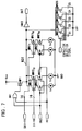
- the interpolator comprises a NAND gate NAND 01 having first and second input terminals IN 1 and IN 2 to which first and second input signal, respectively, are applied; a P-channel MOS transistor MP 1 having its source connected to a power supply VDD and its drain to an internal node N 31 and to the gate of which is input the output signal of the NAND gate NAND 01 ; an inverter INV 3 for switching the logic value of the output signal when the size relationship between the potential at the internal node and a threshold-value voltage changes; inverters INV 1 and INV 2 having first and second input terminals IN 1 and IN 2 to which the first and second input signals, respectively, are applied; 16 N-channel MOS transistors MN 11 1 to MN 11 16 the drains of which are connected in common with the internal node N 31 and the gates of which are connected to control signals SB 1 to SB 16 (complementary signals of S 1 to S 16 ); 16 N-channel MOS transistors MN 12 1 to MN 12 16 the drains of which are
- the plurality of constant-current sources have their other ends connected in common with a power source VSS. Further, a capacitance C is connected between the internal node N 31 and ground (GND).
- the control signals S 1 to S 16 and their complementary signals SB 1 to SB 16 correspond to the control signal C that enters the interpolator 123 from the control circuit 130 in FIG. 1 .
- the current that flows into one of the parallel N-channel MOS transistors of the interpolator be I (the current value of the constant-current source I 0 )
- the threshold-value voltage at which the output of the inverter INV 3 is inverted be V
- CV represent the amount of variation in electric charge up to the threshold-value voltage V.
- N n (n ⁇ 16) holds (n is set by the control signal C), n-number of N-channel MOS transistors MN 21 1 to MN 21 n to the gates of which the inverted signal of the input signal IN 1 is applied turn on for the time T (where T is the timing difference between falling edges of the input signals IN 1 and IN 2 ) after the input signal IN 1 falls to LOW level, as a result of which an electric charge equivalent to n ⁇ I ⁇ T is discharged.
- T the timing difference between falling edges of the input signals IN 1 and IN 2
- Such an interpolator is referred to also as a “16-step interpolator”.
- an interpolator is a P-step (where P is any positive integer) interpolator
- P-number of each of the N-channel MOS transistors MN 11 , MN 12 , MN 21 and MN 22 are disposed in parallel.
- the interpolator shown in FIG. 5 is such that the internal node N 31 is charged to the power-supply potential when the input signals IN 1 , IN 2 are both at HIGH level.
- the input signals IN 1 , IN 2 make a negative-going transition from the high to LOW level, the internal node N 31 is discharged and the output signal rises from the low to HIGH level.
- an arrangement may be adopted in which the output signal rises from the low to HIGH level in response to a positive-going transition of the input signals from the low to HIGH level.
- the inverter INV 3 which is an inverting buffer, should be made a non-inverting buffer.
- FIG. 6 illustrates an example of the circuitry of the interpolator for outputting a rising signal upon dividing the timing difference between edges making a positive-going transition from the low to HIGH level of input signals.
- the interpolator comprises the P-channel MOS transistor MPi having its source connected to the power supply and its drain to the internal node N 31 and to the gate of which is input the output signal of an OR gate OR 1 to the first and second input terminals IN 1 and IN 2 of which the first and second input signals, respectively, are applied; an inverter INV 3 for switching the logic value of the output signal when the size relationship between the potential at the internal node and a threshold-value voltage changes; 16 N-channel MOS transistors MN 11 1 to MN 11 16 the drains of which are connected in common with the internal node N 31 and the gates of which are connected to the control signals SB 1 to SB 16 , respectively; 16 N-channel MOS transistors MN 12 1 to MN 12 16 the drains of which are connected in common with the internal node N 31
- a plurality of series circuits (transistor MN 31 and capacitor C 1 , transistor MN 32 and capacitor C 2 , transistor MN 33 and capacitor 3 , transistor MN 34 and capacitor C 4 , and transistor MN 35 and capacitor C 5 ), each of which comprises a switch element constituted by an N-channel MOS transistor and a capacitor, are connected in parallel between the internal node N 31 and ground, and the switch elements (transistors MN 31 , MN 32 , MN 33 , MN 34 , and MN 35 ) are turned on and off based upon a capacitor selection signal supplied to the control terminals of the switch elements (transistors MN 31 , MN 32 , MN 33 , MN 34 , MN 35 ), whereby a capacitance C applied to the internal node N 31 is set programmably.
- the positions of the N-channel MOS transistors MN 11 and MN 12 and of the N-channel MOS transistors MN 12 and MN 22 may be reversed. More precisely, the drains of N-channel MOS transistors MN 21 1 to NM 21 16 , gates of which are connected in common to the output of the inverter INV 1 , may be connected in common to the internal node N 31 and the drains and sources of the N-channel MOS transistors MN 11 1 to NM 11 16 , gates of which are connected to the control signal terminals SB 1 – 16 , are connected to sources of the N-channel MOS transistors MN 21 1 to NM 21 16 respectively and the ground in common.
- the drains of N-channel MOS transistors MN 22 1 to NM 22 16 may be connected in common to the internal node N 31 and the drains and sources of the N-channel MOS transistors MN 12 1 to NM 12 16 , gates of which are connected to the control signal terminals S 1 – 16 , are connected to sources of the N-channel MOS transistors MN 22 1 to NM 22 16 respectively and the ground in common.
- control signals (weighting signals) SB 1 – 16 may be signals obtained by inverting the signals S 1 – 16 using an inverter.
- the interpolators 123 , 124 and 125 shown in FIG. 4 also employ an interpolator similar to that described with reference to FIGS. 5 to 7 .
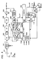
- FIG. 8 is a block diagram illustrating an example of the circuit structure surrounding the phase adjusting circuit 120 of FIG. 1 .
- a 16-step interpolator in the manner shown in FIGS. 5 and 6 constitutes the interpolator 123 .
- the frequency dividing circuit 107 divides the oscillation frequency of the VCO by 16 and outputs a divided signal IN 1 .
- the control circuit 130 On the basis of the count output from the A counter 109 and the cumulative result from arithmetic unit 111 (the output of latch 112 ), the control circuit 130 generates a control signal supplied to the interpolator 123 .
- the control circuit 130 makes a timing control signal WIE active at a predetermined timing and outputs the active signal to the data input terminal of the D-type flip-flop 121 .
- the control circuit 130 activates the timing control signal WIE at the rising edge of the signal IN 1 (the output signal of the ECL/CMOS interface 108 in FIG. 8 )) that corresponds to a ⁇ 32 nd VCO output clock in FIG. 9 and deactivates the signal WIE in response to the signal IN 1 corresponding approximately to the 1000 th clock.
- the D-type flip-flop 121 to the data input terminal of which HIGH level signal WIE is applied, latches the signal WIE and outputs the signal A at the rising edge of the signal IN 1 corresponding to the ⁇ 16 th VCO output clock.
- the D-type flip-flop 122 latches the signal and outputs the signal B at the rising edge of the signal IN 1 corresponding to the ⁇ 16 th VCO output clock.
- the interpolator 123 generates and outputs a signal OUT having a phase obtained by interpolating the timing difference (which corresponds to a period generated by D-type flip-flops 121 , 122 and divided by 16 in the frequency dividing circuit ( 107 ) between the signals A and B at an interior division ratio decided by the control signals S 1 to S 16 , SB 1 to SB 16 supplied from the decoder 115 .
- the interpolator 123 operates and outputs the signal OUT whenever the A counter 109 performs division by A. As a result, the setting of the control signal from the decoder 115 in the interpolator 123 is carried out when the interpolator 123 does not operate.
- control circuit 130 ( 130 A) of this embodiment generates the control signal applied to the interpolator in the phase adjusting circuit 120 ( 120 A).
- FIG. 10 is a diagram useful in describing the control operation of the control circuit 130 shown in FIG. 1 .
- the remainder calculating unit 110 of FIG. 1 is contained in the control circuit 130 .
- the frequency dividing circuit prescaler) 107 includes D-type flip-flops 12 , 13 , 14 and 15 , which construct divide-by-2 frequency dividers, and a D-type flip-flop 11 that constructs a divide-by-2 frequency divider.
- the D-type flip-flops 12 , 13 , 14 and 15 feed the output of the inverting output terminal back to the data input terminal, with the output of the data output terminal of the preceding D-type flip-flop being input to the clock input terminal.
- the D-type flip-flop 11 feeds the output of its inverting output terminal back to its data input terminal and has the output clock of the VCO 106 input to its clock input terminal.
- the timing control signal WIE output from the control circuit 130 is input to an AND gate 131 together with the divided output of the frequency dividing circuit 107 .
- the P-frequency-divided output of the frequency dividing circuit 107 is input to the clock input terminals of the D-type flip-flops 121 and 122 of phase adjusting circuit 120 via the AND gate 131 only when the timing control signal WIE is at HIGH level.
- the AND gate 131 outputs a low-level signal and the P-frequency-divided output of the frequency dividing circuit 107 is not transmitted to the D-type flip-flops 121 and 122 of the phase adjusting circuit 120 .
- the D-type flip-flops 121 and 122 are not supplied with the clock, the interpolator 123 does not operate and less power is consumed. It should be noted that the ECL/CMOS interface 108 in FIG. 2 is omitted from FIG. 10 .
- the output period of the A counter 109 is a ⁇ P or (a+1) ⁇ P.
- the interpolator 123 implements division of the period of its output signal by a ⁇ P+b by making one period of the output of frequency dividing circuit (prescaler) 107 longer than a ⁇ P by the remainder b.
- the interpolator 123 adjusts the phase of the output of frequency dividing circuit 107 by outputting a signal obtained by adding on the phase of the interior division ratio b/P.
- Equation (4) The relationships involving the phase of the output signal of interpolator 123 can be expressed by Equation (4) below.
- C i MOD (C i ⁇ 1 +b,P) is the interior division ratio
- C i ⁇ 1 is the interior division ratio of the preceding period (at the time of the preceding interpolation operation)
- a′ is the frequency-dividing factor of the A counter 109 .
- MOD (p,q) is an operator that represents the remainder r obtained by dividing p by q and corresponds to the remainder calculating circuit 110 (arithmetic circuit 111 and latch 112 in FIG. 3 ) of FIG. 1 .
- B that is input to the arithmetic circuit 111 corresponds to b
- the remainder MOD (C i ⁇ 1 +b,P) that is the result of dividing by P the value obtained by adding b to the value C i ⁇ 1 held in the latch 112 is held in latch 112 as the present value C i of the interior division ratio
- the present value C i of the interior division ratio is supplied to the interpolator 123 as the control signal C.
- the interior division ratio of the interpolator 123 which divides the phase difference between the first and second input signals in steps of P, becomes C i :(P ⁇ C i ), b is added to the preceding value C i ⁇ 1 of the interior division ratio whenever division by a′ is performed (i.e., every period), and the remainder that is the result of dividing the sum by P becomes the present value C i .
- the control circuit 130 sets a value obtained by adding 1 to the frequency dividing factor A of the A counter 109 , the A counter 109 divides by a+1 and this period is made longer than the one period for the case where division was performed originally by a.
- the period of the output signal of interpolator 123 is aP+b at all times and any frequency-dividing factor can be implemented.
- the output period of the frequency dividing circuit 107 is divided equally by P in the interpolator 123 .
- the step for updating the phase of the signal interpolated and output by the interpolator 123 i.e., the difference between the present phase and preceding phase of the interpolated and output signal
- ( b+K/M )/ P ( b ⁇ P+K )/( P ⁇ M )
- the period of the output signal of interpolator 123 is a ⁇ P+b+K/M (where b ⁇ P, K,M hold).
- the output period of the A counter 109 is a ⁇ P or (a+1) ⁇ P.
- the interpolator 123 implements division of the period of its output signal by a ⁇ P+b+K/M by making one period of the output of frequency dividing circuit (prescaler) 107 longer than a ⁇ P by the remainder b+K/M at every period in which the interpolation operation is carried out.
- a correction is performed to add (bP+K) to the interior division ratio of interpolator 123 whose input is the output of the frequency dividing circuit (prescaler) 107 .
- updating of phase at the time of interpolation by the interpolator 123 is performed in steps of (bP+K)/(P ⁇ M).
- Equation (7) The period of the output signal whenever the interpolator 123 interpolates phase is given by Equation (7) below.
- bM and PM represent b ⁇ M and P ⁇ M, respectively.
- C i MOD (C 1 i ⁇ 1 +bM+K,PM) is the interior division ratio
- C 1 i ⁇ 1 is the interior division ratio of the preceding period
- a′ is the frequency-dividing factor of the A counter 109 .
- the interior division ratio of the interpolator 123 is C 1 i :(P ⁇ C 1 i ), b ⁇ M+K is added to the preceding value C 1 i ⁇ 1 of the desired voltage every period (at the divide-by-a′ period, namely whenever the interpolation operation is performed), and the remainder obtained by dividing the result of addition by P ⁇ M becomes C 1 i .
- Equation (8) and (9) The period of the signal output whenever interpolation of phase is performed by the interpolator 123 is given by the Equations (8) and (9) below.
- aP, (a+1)P, bM and PM represent a ⁇ P, (a+1) ⁇ P, b ⁇ M and P ⁇ M, respectively.
- the period of the output signal of interpolator 123 is aP+b+K/M at all times and any fractional frequency-dividing factor can be implemented.
- the output period of the frequency dividing circuit 107 is divided equally by P ⁇ M in the interpolator 123 .
- An interpolator of the kind shown in FIGS. 5 to 7 that inhibits feedthrough current is used as the interpolator.
- another circuit arrangement may be adopted for the interpolator.
- phase difference be divided equally by P ⁇ M (that the step be P ⁇ M) in one interpolator, as a result of which the scale of the interpolator circuitry increases.
- P ⁇ M that the step be P ⁇ M
- each of the parallel-connected N-channel MOS transistors 11 , 12 , 21 and 22 be P ⁇ M in number, result in circuitry of large scale.
- the control signals (S 1 to S 16 and SB 1 to SB 16 ) also require 2 ⁇ P ⁇ M wiring lines and the decoder ( 115 in FIG. 8 ) also become a circuit of large scale.
- the scale of the circuitry can be reduced by adopting a two-stage arrangement of the kind shown in FIG. 11 as the interpolator of phase adjusting circuit 120 .
- the arrangement shown in FIG. 11 corresponds to the arrangement of the embodiment illustrated in FIG. 4 and includes the first and second interpolators 123 and 124 for producing output signals of phases obtained by internally dividing the phase difference of the P-frequency-divided period at interior division ratios C 2 i and C 2 i +1, respectively; and the interpolator 125 for producing an output signal of a phase obtained by performing the interior division of the phase difference 1/P of the output signals of the first and second interpolators at the interior division ratio C 3 i (where the division number of the phase difference is M).
- both the period of the output signal of phase adjusting circuit 120 A and the output period of the A counter 109 are equal to the fractionally divided period described with reference to FIG. 10 . That is, whereas the period of the output signal of interpolator 125 is a ⁇ P+b+K/M ( b ⁇ P, K ⁇ M ) the output period of the A counter 109 is a ⁇ P or (a+1) ⁇ P.
- division by a ⁇ P+b+K/M is implemented by making one period of the output of frequency dividing circuit 107 longer than a ⁇ P by the remainder b+K/M at all times.
- the A counter 109 divides by a
- the P-frequency-divided output of the frequency dividing circuit 107 is subjected to a correction by adding on a phase obtained by internally dividing the output by the interpolator at the interior division ratio (bP+K)/(P ⁇ M).
- C i MOD (C 1 i ⁇ 1 +bM+K,PM) is the interior division ratio
- C 1 i ⁇ 1 is the interior division ratio of the preceding period
- a′ is the frequency-dividing factor of the A counter 109 .
- phase adjusting circuit 120 A having the two-stage interpolator structure is constituted by an interpolator that divides the P-frequency-divided period equally by P and an interpolator that divides the P-frequency-divided period equally by M and division equally by P is carried out by the interpolator of the initial stage, then the interpolator of the succeeding stage performs division equally by M.
- the initial stage is composed of the two interpolators 123 and 124 arranged in parallel, the interior division ratios of which are C 2 i :P ⁇ C 2 i and (C 2 i +1):P ⁇ (C 2 i +1) [where 0 ⁇ C 2 i ⁇ (P ⁇ 1) holds], respectively.
- the interior division ratio of interpolator 125 of the next stage is C 3 i :M ⁇ C 3 i (where 0 ⁇ C 3 i ⁇ M holds).
- C 2 i is an integer obtained by dividing C 1 i by M
- C 3 i is a remainder obtained by dividing C 1 i by M.
- C 2 i INT( C 1 i /M )
- C 3 i MOD( C 1 i ,M ) (11)
- the total interior division ratio of the phase adjusting circuit 120 A is C 1 i :(P ⁇ C 1 i ), b ⁇ M+K is added to the preceding value C 1 i ⁇ 1 of the interior division ratio every period, and the remainder obtained by dividing the result of addition by P ⁇ M is C 1 i .
- the quotient C 2 i and remainder C 3 i obtained by dividing C 1 i by M are found, and signals are obtained by interpolating two signals (that are output from the D-type flip-flops 121 and 122 ), which have a phase difference (P/fvco) of one period of the P-frequency-divided output of the frequency dividing circuit 107 , from two successive pulses of the P-frequency-divided output of the frequency dividing circuit 107 by the two interpolators 123 and 124 , respectively, based upon interior division ratios C 2 i :P ⁇ C 2 i and C 2 i +1:P ⁇ (C 2 i +1), respectively.
- the interior division ratio of the interpolator 125 to which these two signals having this phase difference are input is made C 3 i :M ⁇ C 3 i , and the interpolator 125 produces an output signal C 3 OUT obtained by interpolating the phase difference 1/fvco in accordance with the interior division ratio C 3 i :M ⁇ C 3 i .
- the period of the output signal C 3 OUT of interpolator 125 is equal to that in the case of [2] above and is expressed by Equations (13), (14) below.
- aP, (a+1)P, bM and PM represent a ⁇ P, (a+1) ⁇ P, b ⁇ M and P ⁇ M, respectively.
- the period of the output signal of interpolator 125 is aP+b+K/M at all times and any fractional frequency-dividing factor can be implemented.
- the output period of the frequency dividing circuit 107 is divided equally by PM in the interpolator.
- An interpolator of the kind shown in FIGS. 5 to 7 for example, is utilizable as the interpolator in this arrangement.
- another circuit arrangement may be adopted for the interpolator.
- FIG. 12 is a diagram illustrating the structure of this embodiment.
- the control circuit which is designated by 130 B, has a two-stage structure in conformity with the two-stage structure of the interpolator.
- the output period of the A counter 109 is a ⁇ P or (a+1) ⁇ P.
- control circuit 130 B is made to conform to the two-stage structure of the interpolator.
- Control of the interior division ratio in the control circuit 130 B is expressed by equations (15), and (16) below.
- Equation (16) above corresponds to the first arrangement of the control circuit 130 B, and the interior division ratios of the two parallel interpolators 123 , and 124 of the initial stage are respectively as follows: C 5 i :P ⁇ C 5 i C 5 i +1:P ⁇ (C 5 i +1)
- Equation (15) above corresponds to the second arrangement of the control circuit 130 B, and the interior division ratio of the interpolator 125 of the second stage is as follows: C 4 i :M ⁇ C 4 i
- Equation (17) the output period of the phase adjusting circuit 120 B [the period of the i-th signal and (i ⁇ 1)th signal] is expressed by Equations (17) below.
- aP, (a+1)P, bM and PM represent a ⁇ P, (a+1) ⁇ P, b ⁇ M and P ⁇ M, respectively, and “ ⁇ ” represents multiplication “ ⁇ ”.
- Equation (20) the output period of the phase adjusting circuit 120 B [the period of the i-th signal and (i ⁇ 1)th signal] is expressed by Equation (20) below.
- the output period of the phase adjusting circuit 120 B is a ⁇ P+b+K/M and any fractional frequency-dividing factor can be realized.
- the output period of the prescaler 107 is equally divided by PM in the interpolator.
- An interpolator of the kind shown in FIGS. 5 to 7 is utilizable as the interpolator in this arrangement.
- another circuit arrangement may be adopted for the interpolator.
- the control circuit 130 that sets the interior division ratio of the interpolator in each of the foregoing embodiments will now be described.
- the interpolator In the interval over which the high-speed divided output of the prescaler 107 is divided by A in the A counter 109 [namely the A ⁇ P interval in which the period (1/fvco) of the output clock of VCO 106 serves as the unit], the interpolator is operated only over the interval of one period of the P-frequency-divided output; the interpolator does not operate in the remaining interval.
- the control circuit may be operated in any cycle in which the interpolator does not perform interpolation, as shown in FIG. 13 .
- the timing control signal WIE is output from the control circuit 130 (see FIG. 10 , etc.) and attains HIGH level in FIG. 13
- the P-frequency-divided output of the prescaler 107 are fed to the clock input terminals of the D-type flip-flops 121 and 122 upon passing through the AND gate 131 , and the phase difference between the two signals output from the data output terminals of the D-type flip-flops 121 and 122 is interpolated and output by the interpolator 123 .
- This is the operating interval of the interpolator 123 .
- the control circuit 130 operates at any timing other than in the operating interval of the interpolator 123 , and the control signal that decides the interior division ratio of the next interpolation operation is output to the interpolator 123 .
- the frequency dividing circuit 107 is obtained by cascade-connecting a plurality of simple toggle circuits and the interior division of the output thereof is performed, thereby providing an operation equivalent to that of the conventional modulus control prescaler.
- the arrangement is such that the interpolator 123 (and interpolators 124 and 125 ) and control circuit 130 ( 130 A and 130 B) operate only one time in the interval over which the high-speed divided output of the prescaler 107 is divided by A in the A counter 109 . This reduces power consumption.
- the prescaler 107 is constructed by cascade-connecting toggle circuits. In comparison with the conventional modulus control prescaler, the number of circuit elements is reduced and operation is possible at high speed and with little consumption of power.
- fractional division can be achieved in the same operating cycle as integral division by adjusting the interior division ratio of the interpolator.
- a first frequency dividing circuit for dividing the P-frequency-divided output of the first frequency dividing circuit by A, and an interpolator for outputting a signal having a phase obtained by an interior division of a phase equivalent to one period of the P-frequency-divided output by a fraction whenever division by A is performed, thereby implementing integral frequency division A ⁇ P+B and fractional frequency division A ⁇ P+B+K/M.
- the number of high-speed circuit elements and power consumption are reduced in comparison with the conventional arrangement having two dividing (divide-by-P and divide-by-P+1) prescalers and two counters. Further, in accordance with the present invention, a single programmable counter suffices, thereby reducing power consumption.
- the arrangement is such that the interpolator and control circuit operate only one time in the interval over which the P-frequency-divided output of the first frequency dividing circuit is divided by A.
- control is simplified because there is no longer need for a modulus control signal for changing the frequency-dividing factor of a P/P+1 prescaler.
- the prescaler and control circuit 130 A can be constructed on separate chips, thereby increasing freedom of design.
Landscapes
- Engineering & Computer Science (AREA)
- General Physics & Mathematics (AREA)
- Theoretical Computer Science (AREA)
- Physics & Mathematics (AREA)
- Mathematical Optimization (AREA)
- Mathematical Analysis (AREA)
- Computing Systems (AREA)
- Mathematical Physics (AREA)
- Pure & Applied Mathematics (AREA)
- General Engineering & Computer Science (AREA)
- Computational Mathematics (AREA)
- Stabilization Of Oscillater, Synchronisation, Frequency Synthesizers (AREA)
- Manipulation Of Pulses (AREA)
Abstract
Description
8×3+9=33
N=32×a+b
N=32×(a−b)+33×b
(where a>=b holds) and remainder b can be implemented by an operation dividing by 33 and dividing by 32 the remaining number of times. A pulse-swallow counter is implemented by the combination of two
N=32×(a−b)+33×b
is realized by this series of operations. Thus it is possible to realize any frequency-dividing factor N.
fvco/P
by the
(fvco/P)/A
A×P+(i+1)×(B/P)×P−[i×(B/P)×P]=A×P+B
Hence the frequency-dividing factor N is equal to A×P+B.
(n−1)(aP)+(a+1)P=n(aP+b)
T(16)=CV/(16·I) (1)
T′=(CV−n·I·T)/(16·I) (2)
(a+1)×P.
C i=MOD(C i−1 +b,P)
a′=a+1, if C i−1 +b≧P
a′=a, if C i−1 +b<P (4)
If C i−1 +b≧P holds, then {(a+1)P+(C i /P)P}−(C i−1 /P)P=(a+1)P+(C i−1 +b−P)/P)P−(C i−1 /P)P=aP+b (5)
C i−1 +b<Pholds, then {aP+(C i /P)P}−(C i−1 /P)P=aP+(C i−1 +b)/P)P−(C i−1 /P)P=aP+b (6)
(b+K/M)/P=(b×P+K)/(P×M)
a×P+b+K/M
(where b<P, K,M hold).
C1 i=MOD(C1 i−1 +bM+K,PM)
a′=a+1, if C1 i−1 +bM+K≧PM
a′=a, if C1 i−1 +bM+K<PM (7)
where Ci=MOD (C1 i−1+bM+K,PM) is the interior division ratio, C1 i−1 is the interior division ratio of the preceding period, and a′ is the frequency-dividing factor of the
If C1 i−1 +bM+K≧PM holds, then {(a+1)P+(C1 i /PM)P}−(C1 i−1 /PM)P={(a+1)P+((C1 i−1 +bM+K−PM)/PM)P}−(C1 i−1 /PM)P=aP+b+K/M (8)
C1 i−1 +bM+K<PM holds, then {aP+(C i /PM)P}−(C i−1 /PM)P={aP+((C1 i−1 +bM+K)/PM)P}−(C1 i−1 /PM)P=aP+b+K/M (9)
a×P+b+K/M(b<P, K<M)
the output period of the
(a+1)×P.
C1 i=MOD(C1 i−1 +bM+K,PM)
a′=a+1, if C1 i−1 +bM+K≧PM
a′=a, if C1 i−1 +bM+K<PM (10)
C2 i=INT(C1 i /M)
C3 i=MOD(C1 i ,M) (11)
(C2 i /P)+(C3 i /PM)=(INT(C1 i /M)/P)+(MOD(C1 i ,M)/PM)={(INT(C1 i /M))+(MOD(C1 i ,M)/M)}/P=(C1 i /M)/P=C1 i /MP (12)
If C1 i−1 +bM+K≧PM holds, then {(a+1)P+(C1 i /PM)P}−(C1 i−1 /PM)P=aP+b+K/M (13)
If C1 i−1 +bM+K<PM holds, then {aP+(C i /PM)P}−(C i−1 ,/PM)P=aP+b+K/M (14)
(a+1)×P.
C4 i=MOD(C4 i−1 +K,M)
b′=b+1, if C4 i−1 +K≧M
b′=b, if C4 i−1 +K<M (15)
C5 i=MOD(C5 i−1 +b′,P)
a′=a+1, if C5 i−1 +b′≧P
a′=a, if C5 i−1 +b′<P (16)
C5 i:P−C5 i
C5 i+1:P−(C5 i+1)
C4 i:M−C4 i
{(a+1)P+(C5 i /P)P+(C4 i /PM)P}−{(C5 i−1 /P)P+(C4 i−1 /PM)P}={(a+1)P+(MOD(C5 i−1 +b+1,P)/P)P+(MOD(C4 i−1 +K,M)/PM)P}−{(C5 i−1 /P)P+(C4 i−1 /PM)P}=aP+P·(C5 i−1 +b)/P+P·(C4 i−1 +K/PM)−{(C5 i−1 /P)P+(C4 i−1 /PM)P}=aP+b+K/M (17)
{aP+(C5 i /P)P+(C4 i /PM)P}−{(C5 i−1 /P)P+(C4 i−1 /PM)P}={aP+(MOD(C5 i−1 +b+1,P)/P)P+(MOD(C4 i−1 +K,M)/PM)P}−{(C5 i−1 /P)P+(C4 i−1 /PM)P}=aP+P·(C5 i−1 +b)/P++P·(C4 i−1 +K/PM)−{(C5 i−1 /P)P+(C4 i−1 P/M)P}=aP+b+K/M (18)
{(a+1)P+(C5 i /P)P+(C4 i /PM)P}−{(C5 i−1 /P)P+(C4 i−1 /PM)P}={(a+1)P+(MOD(C5 i−1 +b,P)/P)P+(MOD(C4 i−1 +K,M)/PM)P}−{(C5 i−1 /P)P+(C4 i−1 /PM)P}=aP+P·(C5 i−1 +b)/P+P·(C4 i−1 +K/PM)−{(C5 i−1 /P)P+(C4 i−1 /M)P}=aP+b+K/M (19)
{aP+(C5 i /P)P+(C4 i /PM)P}−{(C5 i−1 /P)P+(C4 i−1 /PM)P}={aP+(MOD(C5 i−1 +b,P)/P)P+(MOD(C4 i−1 +K,M)/PM)P}−{(C5 i−1 /P)P+(C4 i−1 /PM)P}=aP+P·(C5 i−1 +b)/P+P·(C4 i−1 +K/PM)−{(C5 i−1 /P)P+(C4 i−1 P/M)P}=aP+b+K/M (20)
a×P+b+K/M
and any fractional frequency-dividing factor can be realized.
Claims (29)
Applications Claiming Priority (2)
| Application Number | Priority Date | Filing Date | Title |
|---|---|---|---|
| JP2001-273771 | 2001-09-10 | ||
| JP2001273771A JP4587620B2 (en) | 2001-09-10 | 2001-09-10 | Clock control method, frequency dividing circuit and PLL circuit |
Publications (2)
| Publication Number | Publication Date |
|---|---|
| US20030048863A1 US20030048863A1 (en) | 2003-03-13 |
| US7054404B2 true US7054404B2 (en) | 2006-05-30 |
Family
ID=19098938
Family Applications (1)
| Application Number | Title | Priority Date | Filing Date |
|---|---|---|---|
| US10/225,361 Expired - Fee Related US7054404B2 (en) | 2001-09-10 | 2002-08-22 | Clock control method, frequency dividing circuit and PLL circuit |
Country Status (3)
| Country | Link |
|---|---|
| US (1) | US7054404B2 (en) |
| EP (1) | EP1293890A3 (en) |
| JP (1) | JP4587620B2 (en) |
Cited By (17)
| Publication number | Priority date | Publication date | Assignee | Title |
|---|---|---|---|---|
| US20050280474A1 (en) * | 2004-06-16 | 2005-12-22 | Agilent Technologies, Inc. | Method of reducing the fractional spurious and a fractional N-PLL oscillator reducing the fractional spurious |
| US20060076997A1 (en) * | 2004-08-12 | 2006-04-13 | Nec Electronics Corporation | Spread spectrum clock generating apparatus |
| US20070001882A1 (en) * | 2005-07-01 | 2007-01-04 | Realtek Semiconductor Corp. | Method and circuit for producing spread spectrum and/or over clock signal |
| US7323916B1 (en) * | 2005-12-07 | 2008-01-29 | Netlogic Microsystems, Inc. | Methods and apparatus for generating multiple clocks using feedback interpolation |
| US7436921B1 (en) * | 2004-11-05 | 2008-10-14 | Rockwell Collins, Inc. | Frequency sampling phase detector |
| US7532697B1 (en) | 2005-01-27 | 2009-05-12 | Net Logic Microsystems, Inc. | Methods and apparatus for clock and data recovery using a single source |
| US7545188B1 (en) | 2006-08-04 | 2009-06-09 | Integrated Device Technology, Inc | Multiphase clock generator |
| US20110050312A1 (en) * | 2009-08-31 | 2011-03-03 | Nec Electronics Corporation | Multi-phase clock generation circuit |
| US20110228860A1 (en) * | 2010-03-19 | 2011-09-22 | Marc Loinaz | Multi-Value Logic Signaling in Multi-Functional Circuits |
| US20110228889A1 (en) * | 2010-03-19 | 2011-09-22 | Dean Liu | Repeater Architecture with Single Clock Multiplier Unit |
| US8102936B2 (en) | 2002-06-21 | 2012-01-24 | Netlogic Microsystems, Inc. | Methods and apparatus for clock and data recovery using transmission lines |
| US8423814B2 (en) | 2010-03-19 | 2013-04-16 | Netlogic Microsystems, Inc. | Programmable drive strength in memory signaling |
| US8494377B1 (en) | 2010-06-30 | 2013-07-23 | Netlogic Microsystems, Inc. | Systems, circuits and methods for conditioning signals for transmission on a physical medium |
| US8537949B1 (en) | 2010-06-30 | 2013-09-17 | Netlogic Microsystems, Inc. | Systems, circuits and methods for filtering signals to compensate for channel effects |
| US20160087636A1 (en) * | 2014-09-23 | 2016-03-24 | Faraday Technology Corp. | Clock generating apparatus and fractional frequency divider thereof |
| US10116314B1 (en) | 2017-11-01 | 2018-10-30 | Nvidia Corporation | Multi-mode frequency divider |
| US11223363B2 (en) * | 2020-05-28 | 2022-01-11 | Realtek Semiconductor Corporation | Open loop fractional frequency divider |
Families Citing this family (29)
| Publication number | Priority date | Publication date | Assignee | Title |
|---|---|---|---|---|
| JP2005004451A (en) * | 2003-06-11 | 2005-01-06 | Nec Electronics Corp | Spread spectrum clock generation device |
| JP4251640B2 (en) * | 2004-12-17 | 2009-04-08 | インターナショナル・ビジネス・マシーンズ・コーポレーション | Clock generation circuit and method thereof |
| US20060140320A1 (en) * | 2004-12-23 | 2006-06-29 | Jensen Richard S | Mechanism to adjust a clock signal based on embedded clock information |
| US8004268B2 (en) | 2005-09-28 | 2011-08-23 | Nec Corporation | Signal measuring device |
| US7817764B2 (en) * | 2006-09-13 | 2010-10-19 | Sony Corporation | System and method for utilizing a phase interpolator to support a data transmission procedure |
| JP4636107B2 (en) * | 2008-03-31 | 2011-02-23 | ソニー株式会社 | PLL circuit |
| KR100986611B1 (en) | 2008-06-13 | 2010-10-08 | 김영식 | Low power frequency divider and low power phase locked loop having said frequency divider |
| JP5184680B2 (en) * | 2010-09-15 | 2013-04-17 | シャープ株式会社 | Frequency divider circuit, PLL circuit including the same, and semiconductor integrated circuit |
| JP5672092B2 (en) * | 2011-03-17 | 2015-02-18 | 株式会社リコー | Spread spectrum clock generator |
| EP2600529A3 (en) * | 2011-11-30 | 2016-02-24 | Sequans Communications Limited | Control circuitry |
| US8559587B1 (en) * | 2012-03-21 | 2013-10-15 | Integrated Device Technology, Inc | Fractional-N dividers having divider modulation circuits therein with segmented accumulators |
| EP2738629A1 (en) * | 2012-11-30 | 2014-06-04 | EM Microelectronic-Marin SA | High-precision electronic clock movement and method for adjusting a time base |
| JP6155744B2 (en) * | 2013-03-26 | 2017-07-05 | 富士通株式会社 | Clock phase interpolation circuit and data transmission / reception circuit |
| GB2524041A (en) * | 2014-03-12 | 2015-09-16 | Nordic Semiconductor Asa | Frequency synthesizer |
| US9236873B1 (en) | 2014-12-17 | 2016-01-12 | Integrated Device Technology, Inc. | Fractional divider based phase locked loops with digital noise cancellation |
| US9966965B2 (en) * | 2016-06-10 | 2018-05-08 | Silicon Laboratories Inc. | Apparatus for low power signal generator and associated methods |
| US10153777B2 (en) * | 2016-09-30 | 2018-12-11 | Texas Instruments Incorporated | Fractional frequency clock divider with direct division |
| CN107959487B (en) * | 2016-10-14 | 2021-04-09 | 瑞昱半导体股份有限公司 | Phase interpolator and method for generating phase interpolated signal |
| US10855294B2 (en) | 2016-11-08 | 2020-12-01 | Texas Instruments Incorporated | High linearity phase interpolator |
| US10483956B2 (en) | 2017-07-20 | 2019-11-19 | Rohm Co., Ltd. | Phase interpolator, timing generator, and semiconductor integrated circuit |
| JP6902952B2 (en) * | 2017-07-20 | 2021-07-14 | ローム株式会社 | Phase interpolator and timing generator, semiconductor integrated circuit |
| US10637397B2 (en) * | 2017-08-08 | 2020-04-28 | Motorola Solutions, Inc. | Method and apparatus for determining a clock frequency for an electronic processor |
| US10425091B2 (en) * | 2017-10-31 | 2019-09-24 | Texas Instruments Incorporated | Fractional clock generator |
| CN109167597B (en) * | 2018-09-10 | 2023-09-01 | 佛山科学技术学院 | Frequency dividing circuit, frequency dividing device and electronic equipment |
| JP7420537B2 (en) * | 2019-11-26 | 2024-01-23 | ローム株式会社 | phase locked loop circuit |
| US11165432B1 (en) * | 2020-11-06 | 2021-11-02 | Movellus Circuits, Inc. | Glitch-free digital controlled delay line apparatus and method |
| JP2023174194A (en) * | 2022-05-27 | 2023-12-07 | ルネサスエレクトロニクス株式会社 | Semiconductor device |
| CN116820185B (en) * | 2023-08-25 | 2023-11-17 | 高澈科技(上海)有限公司 | Programmable multiphase clock device |
| CN118367900B (en) * | 2024-06-20 | 2024-09-03 | 格创通信(浙江)有限公司 | Phase interpolation circuit and packaging circuit |
Citations (6)
| Publication number | Priority date | Publication date | Assignee | Title |
|---|---|---|---|---|
| US4484153A (en) * | 1981-04-06 | 1984-11-20 | Motorola, Inc. | Voltage converter for a frequency synthesizer |
| JPH0669788A (en) | 1992-08-24 | 1994-03-11 | Matsushita Electric Ind Co Ltd | Pulse swallow system variable frequency divider |
| JPH06120815A (en) | 1992-10-07 | 1994-04-28 | Matsushita Electric Ind Co Ltd | Pulse swallow type variable frequency divider |
| US5349310A (en) * | 1993-06-09 | 1994-09-20 | Alcatel Network Systems, Inc. | Digitally controlled fractional frequency synthesizer |
| US5889437A (en) * | 1997-07-10 | 1999-03-30 | Lg Semicon Co., Ltd. | Frequency synthesizer with low jitter noise |
| US6066990A (en) * | 1997-05-29 | 2000-05-23 | Alcatel | Frequency divider having a prescaler followed by a programmable counter, and a corresponding prescaler and frequency synthesizer |
Family Cites Families (10)
| Publication number | Priority date | Publication date | Assignee | Title |
|---|---|---|---|---|
| US4409564A (en) * | 1981-03-20 | 1983-10-11 | Wavetek | Pulse delay compensation for frequency synthesizer |
| JP2565248B2 (en) * | 1985-11-12 | 1996-12-18 | ソニー株式会社 | Divider circuit |
| JPH03261222A (en) * | 1990-03-09 | 1991-11-21 | Oki Electric Ind Co Ltd | Variable frequency divider |
| US5247469A (en) * | 1991-05-23 | 1993-09-21 | Proxim, Inc. | Digital frequency synthesizer and method with vernier interpolation |
| FR2690022B1 (en) * | 1992-03-24 | 1997-07-11 | Bull Sa | VARIABLE DELAY CIRCUIT. |
| JPH10247850A (en) * | 1997-03-04 | 1998-09-14 | Sony Corp | Frequency-divider circuit |
| JP3649874B2 (en) * | 1997-09-25 | 2005-05-18 | 三洋電機株式会社 | Frequency divider circuit |
| US6188261B1 (en) * | 1998-01-26 | 2001-02-13 | Nippon Telegraph And Telephone Corporation | Programmable delay generator and application circuits having said delay generator |
| JP3789247B2 (en) * | 1999-02-26 | 2006-06-21 | Necエレクトロニクス株式会社 | Clock cycle detection circuit |
| JP3415574B2 (en) * | 2000-08-10 | 2003-06-09 | Necエレクトロニクス株式会社 | PLL circuit |
-
2001
- 2001-09-10 JP JP2001273771A patent/JP4587620B2/en not_active Expired - Fee Related
-
2002
- 2002-08-22 US US10/225,361 patent/US7054404B2/en not_active Expired - Fee Related
- 2002-09-04 EP EP02019919A patent/EP1293890A3/en not_active Withdrawn
Patent Citations (6)
| Publication number | Priority date | Publication date | Assignee | Title |
|---|---|---|---|---|
| US4484153A (en) * | 1981-04-06 | 1984-11-20 | Motorola, Inc. | Voltage converter for a frequency synthesizer |
| JPH0669788A (en) | 1992-08-24 | 1994-03-11 | Matsushita Electric Ind Co Ltd | Pulse swallow system variable frequency divider |
| JPH06120815A (en) | 1992-10-07 | 1994-04-28 | Matsushita Electric Ind Co Ltd | Pulse swallow type variable frequency divider |
| US5349310A (en) * | 1993-06-09 | 1994-09-20 | Alcatel Network Systems, Inc. | Digitally controlled fractional frequency synthesizer |
| US6066990A (en) * | 1997-05-29 | 2000-05-23 | Alcatel | Frequency divider having a prescaler followed by a programmable counter, and a corresponding prescaler and frequency synthesizer |
| US5889437A (en) * | 1997-07-10 | 1999-03-30 | Lg Semicon Co., Ltd. | Frequency synthesizer with low jitter noise |
Cited By (30)
| Publication number | Priority date | Publication date | Assignee | Title |
|---|---|---|---|---|
| US8599983B2 (en) | 2002-06-21 | 2013-12-03 | Netlogic Microsystems, Inc. | Methods and apparatus for clock and data recovery using transmission lines |
| US8102936B2 (en) | 2002-06-21 | 2012-01-24 | Netlogic Microsystems, Inc. | Methods and apparatus for clock and data recovery using transmission lines |
| US8155236B1 (en) | 2002-06-21 | 2012-04-10 | Netlogic Microsystems, Inc. | Methods and apparatus for clock and data recovery using transmission lines |
| US20050280474A1 (en) * | 2004-06-16 | 2005-12-22 | Agilent Technologies, Inc. | Method of reducing the fractional spurious and a fractional N-PLL oscillator reducing the fractional spurious |
| US20060076997A1 (en) * | 2004-08-12 | 2006-04-13 | Nec Electronics Corporation | Spread spectrum clock generating apparatus |
| US7436921B1 (en) * | 2004-11-05 | 2008-10-14 | Rockwell Collins, Inc. | Frequency sampling phase detector |
| US7236039B2 (en) * | 2004-12-08 | 2007-06-26 | Nec Electronics Corporation | Spread spectrum clock generating apparatus |
| US7532697B1 (en) | 2005-01-27 | 2009-05-12 | Net Logic Microsystems, Inc. | Methods and apparatus for clock and data recovery using a single source |
| US7495496B2 (en) * | 2005-07-01 | 2009-02-24 | Realtek Semiconductor Corp. | Method and circuit for producing spread spectrum and/or over clock signal |
| US20070001882A1 (en) * | 2005-07-01 | 2007-01-04 | Realtek Semiconductor Corp. | Method and circuit for producing spread spectrum and/or over clock signal |
| US20080260071A1 (en) * | 2005-12-07 | 2008-10-23 | Stefanos Sidiropoulos | Methods and Apparatus for Frequency Synthesis with Feedback Interpolation |
| US7443215B1 (en) * | 2005-12-07 | 2008-10-28 | Netlogic Microsystems, Inc. | Methods and apparatus to increase the resolution of a clock synthesis circuit that uses feedback interpolation |
| US8667038B1 (en) | 2005-12-07 | 2014-03-04 | Netlogic Microsystems, Inc. | Methods and apparatus to increase the resolution of a clock synthesis circuit that uses feedback interpolation |
| US8433018B2 (en) * | 2005-12-07 | 2013-04-30 | Netlogic Microsystems, Inc. | Methods and apparatus for frequency synthesis with feedback interpolation |
| US7323916B1 (en) * | 2005-12-07 | 2008-01-29 | Netlogic Microsystems, Inc. | Methods and apparatus for generating multiple clocks using feedback interpolation |
| US7545188B1 (en) | 2006-08-04 | 2009-06-09 | Integrated Device Technology, Inc | Multiphase clock generator |
| US20110050312A1 (en) * | 2009-08-31 | 2011-03-03 | Nec Electronics Corporation | Multi-phase clock generation circuit |
| US8423814B2 (en) | 2010-03-19 | 2013-04-16 | Netlogic Microsystems, Inc. | Programmable drive strength in memory signaling |
| US8520744B2 (en) | 2010-03-19 | 2013-08-27 | Netlogic Microsystems, Inc. | Multi-value logic signaling in multi-functional circuits |
| US8638896B2 (en) | 2010-03-19 | 2014-01-28 | Netlogic Microsystems, Inc. | Repeate architecture with single clock multiplier unit |
| US20110228889A1 (en) * | 2010-03-19 | 2011-09-22 | Dean Liu | Repeater Architecture with Single Clock Multiplier Unit |
| US20110228860A1 (en) * | 2010-03-19 | 2011-09-22 | Marc Loinaz | Multi-Value Logic Signaling in Multi-Functional Circuits |
| US9094020B2 (en) | 2010-03-19 | 2015-07-28 | Broadcom Corporation | Multi-value logic signaling in multi-functional circuits |
| US8494377B1 (en) | 2010-06-30 | 2013-07-23 | Netlogic Microsystems, Inc. | Systems, circuits and methods for conditioning signals for transmission on a physical medium |
| US8537949B1 (en) | 2010-06-30 | 2013-09-17 | Netlogic Microsystems, Inc. | Systems, circuits and methods for filtering signals to compensate for channel effects |
| US8948331B2 (en) | 2010-06-30 | 2015-02-03 | Netlogic Microsystems, Inc. | Systems, circuits and methods for filtering signals to compensate for channel effects |
| US20160087636A1 (en) * | 2014-09-23 | 2016-03-24 | Faraday Technology Corp. | Clock generating apparatus and fractional frequency divider thereof |
| US9385733B2 (en) * | 2014-09-23 | 2016-07-05 | Faraday Technology Corp. | Clock generating apparatus and fractional frequency divider thereof |
| US10116314B1 (en) | 2017-11-01 | 2018-10-30 | Nvidia Corporation | Multi-mode frequency divider |
| US11223363B2 (en) * | 2020-05-28 | 2022-01-11 | Realtek Semiconductor Corporation | Open loop fractional frequency divider |
Also Published As
| Publication number | Publication date |
|---|---|
| EP1293890A2 (en) | 2003-03-19 |
| JP4587620B2 (en) | 2010-11-24 |
| JP2003087113A (en) | 2003-03-20 |
| EP1293890A3 (en) | 2007-05-09 |
| US20030048863A1 (en) | 2003-03-13 |
Similar Documents
| Publication | Publication Date | Title |
|---|---|---|
| US7054404B2 (en) | Clock control method, frequency dividing circuit and PLL circuit | |
| US6614319B2 (en) | Phase-locked loop circuit of fractional frequency-dividing type | |
| JP3653892B2 (en) | Fractional N frequency synthesizer | |
| JP3388527B2 (en) | Fractional-N frequency divider and fractional-N frequency synthesizer using the same | |
| US7103855B2 (en) | Clock control circuit and method | |
| US8081018B2 (en) | Low power radio frequency divider | |
| US6411669B1 (en) | Dual-modulus prescaler for RF synthesizer | |
| US6794944B2 (en) | Lock detection circuit | |
| US6903615B2 (en) | Digitally-controlled oscillator with switched-capacitor frequency selection | |
| US6829318B2 (en) | PLL synthesizer that uses a fractional division value | |
| US5614869A (en) | High speed divider for phase-locked loops | |
| EP0954106B1 (en) | Clock signal multiplier circuit for a clock signal generator circuit | |
| US7372340B2 (en) | Precision frequency and phase synthesis with fewer voltage-controlled oscillator stages | |
| US11171654B1 (en) | Delay locked loop with segmented delay circuit | |
| US7332945B2 (en) | Divider having dual modulus pre-scaler and an associated method | |
| EP1518323B1 (en) | Phase-locked loop with incremental phase detectors and a converter for combining a logical operation with a digital to analog conversion | |
| CN111786668B (en) | Dual-mode prescaler | |
| JP2003229761A (en) | Counter circuit and pll circuit using the same | |
| Deng | Building Blocks for A Wide-Band Phase-Locked Loop |
Legal Events
| Date | Code | Title | Description |
|---|---|---|---|
| AS | Assignment |
Owner name: NEC CORPORATION, JAPAN Free format text: ASSIGNMENT OF ASSIGNORS INTEREST;ASSIGNOR:SAEKI, TAKANORI;REEL/FRAME:013222/0566 Effective date: 20020815 |
|
| AS | Assignment |
Owner name: NEC ELECTRONICS CORPORATION, JAPAN Free format text: ASSIGNMENT OF ASSIGNORS INTEREST;ASSIGNOR:NEC CORPORATION;REEL/FRAME:013800/0228 Effective date: 20021101 |
|
| FEPP | Fee payment procedure |
Free format text: PAYOR NUMBER ASSIGNED (ORIGINAL EVENT CODE: ASPN); ENTITY STATUS OF PATENT OWNER: LARGE ENTITY |
|
| FPAY | Fee payment |
Year of fee payment: 4 |
|
| AS | Assignment |
Owner name: RENESAS ELECTRONICS CORPORATION, JAPAN Free format text: CHANGE OF NAME;ASSIGNOR:NEC ELECTRONICS CORPORATION;REEL/FRAME:025486/0561 Effective date: 20100401 |
|
| REMI | Maintenance fee reminder mailed | ||
| LAPS | Lapse for failure to pay maintenance fees | ||
| STCH | Information on status: patent discontinuation |
Free format text: PATENT EXPIRED DUE TO NONPAYMENT OF MAINTENANCE FEES UNDER 37 CFR 1.362 |
|
| FP | Lapsed due to failure to pay maintenance fee |
Effective date: 20140530 |