US7022550B2 - Methods for forming aluminum-containing p-contacts for group III-nitride light emitting diodes - Google Patents
Methods for forming aluminum-containing p-contacts for group III-nitride light emitting diodes Download PDFInfo
- Publication number
- US7022550B2 US7022550B2 US10/819,740 US81974004A US7022550B2 US 7022550 B2 US7022550 B2 US 7022550B2 US 81974004 A US81974004 A US 81974004A US 7022550 B2 US7022550 B2 US 7022550B2
- Authority
- US
- United States
- Prior art keywords
- layer
- group iii
- type group
- nitride layer
- forming
- Prior art date
- Legal status (The legal status is an assumption and is not a legal conclusion. Google has not performed a legal analysis and makes no representation as to the accuracy of the status listed.)
- Expired - Lifetime
Links
Images


Classifications
-
- H—ELECTRICITY
- H10—SEMICONDUCTOR DEVICES; ELECTRIC SOLID-STATE DEVICES NOT OTHERWISE PROVIDED FOR
- H10H—INORGANIC LIGHT-EMITTING SEMICONDUCTOR DEVICES HAVING POTENTIAL BARRIERS
- H10H20/00—Individual inorganic light-emitting semiconductor devices having potential barriers, e.g. light-emitting diodes [LED]
- H10H20/80—Constructional details
- H10H20/81—Bodies
- H10H20/822—Materials of the light-emitting regions
- H10H20/824—Materials of the light-emitting regions comprising only Group III-V materials, e.g. GaP
- H10H20/825—Materials of the light-emitting regions comprising only Group III-V materials, e.g. GaP containing nitrogen, e.g. GaN
-
- H—ELECTRICITY
- H10—SEMICONDUCTOR DEVICES; ELECTRIC SOLID-STATE DEVICES NOT OTHERWISE PROVIDED FOR
- H10H—INORGANIC LIGHT-EMITTING SEMICONDUCTOR DEVICES HAVING POTENTIAL BARRIERS
- H10H20/00—Individual inorganic light-emitting semiconductor devices having potential barriers, e.g. light-emitting diodes [LED]
- H10H20/80—Constructional details
- H10H20/83—Electrodes
- H10H20/832—Electrodes characterised by their material
- H10H20/835—Reflective materials
-
- H—ELECTRICITY
- H10—SEMICONDUCTOR DEVICES; ELECTRIC SOLID-STATE DEVICES NOT OTHERWISE PROVIDED FOR
- H10H—INORGANIC LIGHT-EMITTING SEMICONDUCTOR DEVICES HAVING POTENTIAL BARRIERS
- H10H20/00—Individual inorganic light-emitting semiconductor devices having potential barriers, e.g. light-emitting diodes [LED]
- H10H20/01—Manufacture or treatment
- H10H20/032—Manufacture or treatment of electrodes
-
- H—ELECTRICITY
- H10—SEMICONDUCTOR DEVICES; ELECTRIC SOLID-STATE DEVICES NOT OTHERWISE PROVIDED FOR
- H10H—INORGANIC LIGHT-EMITTING SEMICONDUCTOR DEVICES HAVING POTENTIAL BARRIERS
- H10H20/00—Individual inorganic light-emitting semiconductor devices having potential barriers, e.g. light-emitting diodes [LED]
- H10H20/80—Constructional details
- H10H20/81—Bodies
- H10H20/819—Bodies characterised by their shape, e.g. curved or truncated substrates
-
- H—ELECTRICITY
- H10—SEMICONDUCTOR DEVICES; ELECTRIC SOLID-STATE DEVICES NOT OTHERWISE PROVIDED FOR
- H10H—INORGANIC LIGHT-EMITTING SEMICONDUCTOR DEVICES HAVING POTENTIAL BARRIERS
- H10H20/00—Individual inorganic light-emitting semiconductor devices having potential barriers, e.g. light-emitting diodes [LED]
- H10H20/80—Constructional details
- H10H20/83—Electrodes
- H10H20/831—Electrodes characterised by their shape
-
- H—ELECTRICITY
- H10—SEMICONDUCTOR DEVICES; ELECTRIC SOLID-STATE DEVICES NOT OTHERWISE PROVIDED FOR
- H10W—GENERIC PACKAGES, INTERCONNECTIONS, CONNECTORS OR OTHER CONSTRUCTIONAL DETAILS OF DEVICES COVERED BY CLASS H10
- H10W72/00—Interconnections or connectors in packages
- H10W72/01—Manufacture or treatment
- H10W72/019—Manufacture or treatment of bond pads
-
- H—ELECTRICITY
- H10—SEMICONDUCTOR DEVICES; ELECTRIC SOLID-STATE DEVICES NOT OTHERWISE PROVIDED FOR
- H10W—GENERIC PACKAGES, INTERCONNECTIONS, CONNECTORS OR OTHER CONSTRUCTIONAL DETAILS OF DEVICES COVERED BY CLASS H10
- H10W72/00—Interconnections or connectors in packages
- H10W72/071—Connecting or disconnecting
- H10W72/072—Connecting or disconnecting of bump connectors
- H10W72/07251—Connecting or disconnecting of bump connectors characterised by changes in properties of the bump connectors during connecting
- H10W72/07252—Connecting or disconnecting of bump connectors characterised by changes in properties of the bump connectors during connecting changes in structures or sizes
-
- H—ELECTRICITY
- H10—SEMICONDUCTOR DEVICES; ELECTRIC SOLID-STATE DEVICES NOT OTHERWISE PROVIDED FOR
- H10W—GENERIC PACKAGES, INTERCONNECTIONS, CONNECTORS OR OTHER CONSTRUCTIONAL DETAILS OF DEVICES COVERED BY CLASS H10
- H10W72/00—Interconnections or connectors in packages
- H10W72/20—Bump connectors, e.g. solder bumps or copper pillars; Dummy bumps; Thermal bumps
- H10W72/221—Structures or relative sizes
- H10W72/227—Multiple bumps having different sizes
-
- H—ELECTRICITY
- H10—SEMICONDUCTOR DEVICES; ELECTRIC SOLID-STATE DEVICES NOT OTHERWISE PROVIDED FOR
- H10W—GENERIC PACKAGES, INTERCONNECTIONS, CONNECTORS OR OTHER CONSTRUCTIONAL DETAILS OF DEVICES COVERED BY CLASS H10
- H10W72/00—Interconnections or connectors in packages
- H10W72/90—Bond pads, in general
- H10W72/921—Structures or relative sizes of bond pads
- H10W72/923—Bond pads having multiple stacked layers
-
- H—ELECTRICITY
- H10—SEMICONDUCTOR DEVICES; ELECTRIC SOLID-STATE DEVICES NOT OTHERWISE PROVIDED FOR
- H10W—GENERIC PACKAGES, INTERCONNECTIONS, CONNECTORS OR OTHER CONSTRUCTIONAL DETAILS OF DEVICES COVERED BY CLASS H10
- H10W72/00—Interconnections or connectors in packages
- H10W72/90—Bond pads, in general
- H10W72/921—Structures or relative sizes of bond pads
- H10W72/926—Multiple bond pads having different sizes
-
- H—ELECTRICITY
- H10—SEMICONDUCTOR DEVICES; ELECTRIC SOLID-STATE DEVICES NOT OTHERWISE PROVIDED FOR
- H10W—GENERIC PACKAGES, INTERCONNECTIONS, CONNECTORS OR OTHER CONSTRUCTIONAL DETAILS OF DEVICES COVERED BY CLASS H10
- H10W72/00—Interconnections or connectors in packages
- H10W72/90—Bond pads, in general
- H10W72/941—Dispositions of bond pads
- H10W72/9415—Dispositions of bond pads relative to the surface, e.g. recessed, protruding
-
- H—ELECTRICITY
- H10—SEMICONDUCTOR DEVICES; ELECTRIC SOLID-STATE DEVICES NOT OTHERWISE PROVIDED FOR
- H10W—GENERIC PACKAGES, INTERCONNECTIONS, CONNECTORS OR OTHER CONSTRUCTIONAL DETAILS OF DEVICES COVERED BY CLASS H10
- H10W72/00—Interconnections or connectors in packages
- H10W72/90—Bond pads, in general
- H10W72/941—Dispositions of bond pads
- H10W72/944—Dispositions of multiple bond pads
-
- H—ELECTRICITY
- H10—SEMICONDUCTOR DEVICES; ELECTRIC SOLID-STATE DEVICES NOT OTHERWISE PROVIDED FOR
- H10W—GENERIC PACKAGES, INTERCONNECTIONS, CONNECTORS OR OTHER CONSTRUCTIONAL DETAILS OF DEVICES COVERED BY CLASS H10
- H10W72/00—Interconnections or connectors in packages
- H10W72/90—Bond pads, in general
- H10W72/951—Materials of bond pads
- H10W72/952—Materials of bond pads comprising metals or metalloids, e.g. PbSn, Ag or Cu
Definitions
- the following relates to the lighting arts. It especially relates to flip-chip bonded group III-nitride light emitting diodes for lighting applications, and will be described with particular reference thereto. However, the following also finds application in conjunction with other types of group III-nitride light emitting diodes, and in other group III-nitride optoelectronic devices such as vertical cavity surface emitting lasers (VCSELs).
- VCSELs vertical cavity surface emitting lasers
- a light emitting diode with a light-transmissive substrate is bonded “face down” to bonding bumps of a mount, that is, with the epitaxial layers proximate to the mount and the light-transmissive substrate distal from the mount, to make electrical and mechanical connection to the mount.
- the flip-chip arrangement has a number of advantages, including improved thermal heat sinking due to the proximity of the front-side active layers to the heat sinking mount, and elimination of electrode shadowing losses.
- Aluminum has the advantage of being highly reflective; however, aluminum has a low work function and a large contact resistance with respect to p-type gallium nitride.
- a nickel layer is sometimes inserted between the p-type gallium nitride and the aluminum to improve electrical characteristics. While having good electrical characteristics, such nickel/aluminum contacts still exhibit less than ideal reflectance characteristics due to light absorption in the nickel.
- the present invention provides a new p-contact and method for making a p-contact that overcomes the above-referenced problems and others.
- a flip-chip LED device comprises a plurality of group III-nitride semiconductor layers defining a p/n junction and including a top p-type group III-nitride layer, and a p-contact for flip-chip bonding the top p-type group III-nitride layer.
- the p-contact includes an aluminum layer disposed on the top p-type group III-nitride layer, and an interface layer disposed between the aluminum layer and the top p-type group III-nitride layer.
- the interface layer reduces a contact resistance between the aluminum layer and the top p-type group III-nitride layer.
- the interface layer comprises one or more group III-nitride layers.
- a method for forming a p-contact on a top p-type group III-nitride layer of a flip-chip LED device.
- An interface layer is formed on the top p-type group III-nitride layer.
- An aluminum layer is formed on the interface layer. The interface layer reduces a contact resistance between the aluminum layer and the top p-type group III-nitride layer.
- a method for forming a p-contact on a top p-type group III-nitride layer of a flip-chip LED device.
- the top p-type group III-nitride layer is exposed to hydrochloric acid.
- the top p-type group III-nitride layer is exposed to a piranha solution.
- an aluminum layer is disposed on the top p-type group III-nitride layer.
- the application may take form in various components and arrangements of components, and in various process operations and arrangements of process operations.
- the drawings are only for purposes of illustrating preferred embodiments and are not to be construed as limiting the application.
- FIG. 1 shows a cross-sectional view of a flip-chip light emitting diode including an improved p-contact.
- FIG. 2 shows a cross-sectional view of another embodiment of a p-contact which employs a tunnel junction.
- FIG. 3 shows a cross-sectional view of yet another embodiment of a p-contact which employs an interposed p-InGaN layer.
- FIG. 4 compares measurements of brightness of white LEDs fabricated with nickel/aluminum based contacts (left hand side) with white LEDs fabricated from the same epitaxial wafer with aluminum contacts but otherwise similar device fabrication processing (right hand side).
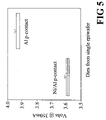
- FIG. 5 compares measurements of the device voltage of white LEDs fabricated with nickel/aluminum based contacts (left hand side) with white LEDs fabricated from the same epitaxial wafer with aluminum contacts but otherwise similar device fabrication processing (right hand side).
- a flip-chip light emitting diode device 10 includes a light emitting diode die 12 mounted in a flip-chip fashion to a mount 14 .
- the light emitting diode die 12 includes a light-transmissive substrate 20 , which is, preferably, a substantially transparent sapphire or silicon carbide substrate.
- a plurality of semiconductor layers 22 are formed on the light-transmissive substrate 20 by metalorganic chemical vapor deposition (also referred to as organometallic vapor phase epitaxy and similar nomenclatures), molecular beam epitaxy, chemical beam epitaxy, or another epitaxial film deposition technique.
- the semiconductor layers 22 are selected from the group III-nitride layers such as GaN layers, AlN layers, InN layers, and ternary and quaternary alloys thereof.
- the substrate is used as an epitaxy template for forming the semiconductor layers 22 and is subsequently thinned or removed in the final device. In such embodiments where the substrate is ultimately thinned or removed, the substrate can be opaque.
- the semiconductor layers 22 define a light emitting structure that emits light when electrically energized.
- the semiconductor layers 22 include an n-type group III-nitride layer 24 , such as an n-type GaN layer or aluminum gallium nitride (AlGaN) layer, an active region 26 , and a top p-type group III-nitride layer 28 , which is typically made of gallium nitride or a aluminum gallium nitride.
- the active region 26 includes a single layer of InN, GaN, In x Ga 1-x N (0 ⁇ x ⁇ 1) or the like.
- the active region 26 includes a plurality of layers defining, for example, a single- or multiple-quantum well or superlattice active region.
- a group III-nitride-based structure typically emits light in the blue to ultraviolet spectral range, with the specific emission spectrum dependent upon the layer compositions, thicknesses, presence of certain impurities, and other features.
- the semiconductor layers 22 include additional layers, such as Al x Ga 1-x N cladding layers, a current-spreading layer, a buffer layer for promoting epitaxial growth, or the like.
- the device die is another type of optoelectronic device, such as a vertical cavity surface emitting laser (VCSEL).
- VCSEL vertical cavity surface emitting laser
- the p-contact 30 is generally a multiple layer stack, including an aluminum layer 32 and a bonding stack 34 .
- the layers 32 , 34 are deposited in a single deposition process or in multiple deposition processes. Substantially any suitable thin film deposition technique or combination of techniques, such as thermal evaporation, electron beam evaporation, sputtering, electroplating, or the like can be employed.
- an n-type contact 36 is defined and the device is optionally protected with a dielectric layer (not shown) having windows through which the electrodes 30 , 36 are exposed.
- the top p-type group III-nitride layer 28 is a p-GaN layer, a p-AlGaN layer, or another relatively large-bandgap group III-nitride material.
- the semiconductor layers 22 are lithographically processed to remove portions of the active region 26 and the top p-type group III-nitride layer 28 to define device mesas, and the contact electrodes 30 , 36 are formed.
- Aluminum has a relatively low work function, and forms a relatively high resistance contact to the top p-type group III-nitride layer 28 .
- a piranha solution is a solution of sulfuric acid, hydrogen peroxide, and optionally deionized water.
- the surface preparation of the top p-type group III-nitride layer 28 includes: (i) a 10 minute exposure to pure hydrochloric acid (HCl) at 50° C. and a rinse in deionized water (DI); followed by (ii) a 2 minute exposure to a 10:1:1 sulfuric acid:hydrogen peroxide:water piranha solution.
- the exposure to the piranha solution is performed at room temperature; however, exothermic reactions during the exposure generally produce some heating.
- the surface of the top p-type group III-nitride layer 28 is again rinsed in DI.
- the HCl/piranha surface preparation of the top p-type group III-nitride layer results in a reduced contact resistance of the p-contact 30 .
- the HCl/piranha processing produces a modification of the surface of the top p-type group III-nitride layer 28 to form an interface layer 40 between the top p-type group III-nitride layer 28 and the aluminum layer 32 which reduces the electrical barrier between the top p-type group III-nitride layer 28 and the subsequently deposited aluminum 32 . It is believed that this modified surface may involve more pure (i.e., less contaminated) surface of the top p-type group III-nitride layer 28 , or may involve a chemical or structural modification of the surface of the top p-type group III-nitride layer 28 .
- the interface layer 40 comprises one or more group III-nitride layers
- those layers may be as thin as a few monolayers, may represent a more clean group III-nitride interface layer than is achieved without the HCl/piranha surface preparation, or may represent a roughened or otherwise structurally modified group III-nitride/aluminum interface layer.
- the bonding stack 34 is preferably a multiple layer metal stack, including an adhesion layer 50 , a diffusion-blocking layer 52 , and a bonding layer 54 .
- the adhesion layer 50 is titanium
- the bonding layer 54 is gold, which provides a good bonding surface for a variety of bonding methods.
- the diffusion-blocking layer 52 is preferably a platinum layer.
- the diffusion-blocking layer 52 is preferably nickel.
- the bonding stack 34 might be a single layer, two layers, or more than three layers, which might include one or more materials such as gold, titanium, nickel, platinum, or other.
- the aluminum layer 32 may provide a good bonding surface, in which cases the bonding stack 34 may be omitted.
- the flip-chip light emitting diode die 12 is bonded to bonding pads 56 , 58 that laterally align with the contacts 30 , 36 .
- the bonding is performed by one or more solder bumps 60 , 62 , by thermosonic bonding to gold-coated copper bumps, or the like.
- the bonding bump 60 that secures the p-type electrode 30 is an array of bonding bumps laterally distributed to conform to the area of the p-type contact 30 .
- the semiconductor layers 22 include a tunnel junction 66 deposited on the top p-type group III-nitride layer 28 during the growth of the semiconductor layers 22 .
- the tunnel junction includes a degenerately doped p-type group III-nitride layer 68 deposited on the p-type group III-nitride layer 28 and a degenerately doped n-type layer 70 deposited on the degenerately doped p-type group III-nitride layer 68 .
- degenerately doped layers 68 , 70 are preferably gallium nitride layers, although some indium can also be alloyed in to form lower bandgap indium gallium nitride degenerate layers.
- the tunnel junction 66 is preferably thin, such as a few nanometers thickness or less for each degenerate layer 68 , 70 . Hence, some increased light absorption due to indium alloying may be acceptable.
- An n-type group III-nitride layer 72 is deposited on the tunnel junction 66 , and the aluminum layer 32 is formed on the n-type gallium nitride layer 72 .
- the bonding stack 34 is optionally formed on the aluminum layer 32 as before.
- the n-type group III-nitride layer 72 is an n-GaN layer. Alloying aluminum into the n-type group III-nitride layer 72 to form AlGaN reduces optical absorption in the layer, but increases the bandgap which can degrade the quality of the electrical contact. Alloying indium into the n-type group III-nitride layer 72 to form InGaN increases optical absorption in the layer, but advantageously decreases the bandgap which generally improves the quality of the electrical contact.
- the p-contact 30 ′ operates as follows.
- the tunnel junction 66 provides non-rectifying and preferably quasi-ohmic electrical communication between the top p-type group III-nitride layer 28 and the n-type gallium nitride layer 72 .
- the contact resistance between the aluminum layer 32 and the n-type gallium nitride layer 72 is relatively low, and so the overall p-contact 30 ′ exhibits improved electrical characteristics.
- the semiconductor layers 22 include a p-type indium gallium nitride (InGaN) layer 80 deposited on the top p-type group III-nitride layer 28 during the growth of the semiconductor layers 22 .
- the layer 80 is preferably kept thin, such as a few nanometers or tens of nanometers thick.
- the aluminum layer 32 is formed on the p-type InGaN layer 80 .
- the bonding stack 34 is optionally formed on the aluminum layer 32 as before.
- the p-contact 30 ′′ operates as follows.
- the low bandgap InGaN 80 reduces the electrical barrier between the InGaN 80 and the aluminum layer 32 versus direct deposition of the aluminum on gallium nitride.
- the reduced barrier provides more quasi-ohmic electrical communication between the top p-type group III-nitride layer 28 and the aluminum layer 32 , and so the overall p-contact 30 ′′ exhibits improved electrical characteristics.
- the HCl/piranha surface processing is optionally applied prior to forming the aluminum layer 32 , to further improve electrical characteristics of the p-contact.
- white LED lamps having traditional nickel/aluminum based p-contacts are experimentally compared with LED lamps in which the nickel/aluminum based p-contact was replaced with the aluminum based p-contact 30 .
- the devices with nickel/aluminum and aluminum p-contacts were fabricated from dice cleaved from the same epitaxial wafer having blue light-emitting epitaxial layers, using identical fabrication processes except for the p-contact fabrication. The dice were similarly mounted, epoxy-encapsulated, and phosphorized using a yellow phosphor that converts some of the blue electroluminescence into yellow light to approximate white light.
- the brightness of the white LED was increased by 50% by replacing the nickel/aluminum p-contact with the aluminum p-contact.
- the HCl/piranha surface processing limits the increase in the device forward voltage due to electrical resistance to about 0.3V.
- the luminous efficiency (output lumens/input electrical power) increased on average by 34%.
Landscapes
- Led Devices (AREA)
- Led Device Packages (AREA)
Abstract
Description
Claims (14)
Priority Applications (4)
| Application Number | Priority Date | Filing Date | Title |
|---|---|---|---|
| US10/819,740 US7022550B2 (en) | 2004-04-07 | 2004-04-07 | Methods for forming aluminum-containing p-contacts for group III-nitride light emitting diodes |
| PCT/US2005/011967 WO2005101498A2 (en) | 2004-04-07 | 2005-04-07 | HIGH REFLECTIVITY P-CONTACT FOR InGaN LEDs |
| TW094111006A TWI449201B (en) | 2004-04-07 | 2005-04-07 | High reflectivity P contact of indium gallium nitride light-emitting diode |
| US11/387,157 US20060186552A1 (en) | 2004-04-07 | 2006-03-23 | High reflectivity p-contacts for group lll-nitride light emitting diodes |
Applications Claiming Priority (1)
| Application Number | Priority Date | Filing Date | Title |
|---|---|---|---|
| US10/819,740 US7022550B2 (en) | 2004-04-07 | 2004-04-07 | Methods for forming aluminum-containing p-contacts for group III-nitride light emitting diodes |
Related Child Applications (1)
| Application Number | Title | Priority Date | Filing Date |
|---|---|---|---|
| US11/387,157 Division US20060186552A1 (en) | 2004-04-07 | 2006-03-23 | High reflectivity p-contacts for group lll-nitride light emitting diodes |
Publications (2)
| Publication Number | Publication Date |
|---|---|
| US20050224990A1 US20050224990A1 (en) | 2005-10-13 |
| US7022550B2 true US7022550B2 (en) | 2006-04-04 |
Family
ID=35059784
Family Applications (2)
| Application Number | Title | Priority Date | Filing Date |
|---|---|---|---|
| US10/819,740 Expired - Lifetime US7022550B2 (en) | 2004-04-07 | 2004-04-07 | Methods for forming aluminum-containing p-contacts for group III-nitride light emitting diodes |
| US11/387,157 Abandoned US20060186552A1 (en) | 2004-04-07 | 2006-03-23 | High reflectivity p-contacts for group lll-nitride light emitting diodes |
Family Applications After (1)
| Application Number | Title | Priority Date | Filing Date |
|---|---|---|---|
| US11/387,157 Abandoned US20060186552A1 (en) | 2004-04-07 | 2006-03-23 | High reflectivity p-contacts for group lll-nitride light emitting diodes |
Country Status (3)
| Country | Link |
|---|---|
| US (2) | US7022550B2 (en) |
| TW (1) | TWI449201B (en) |
| WO (1) | WO2005101498A2 (en) |
Cited By (6)
| Publication number | Priority date | Publication date | Assignee | Title |
|---|---|---|---|---|
| US20060006506A1 (en) * | 2004-07-09 | 2006-01-12 | Kabushiki Kaisha Toshiba | Semiconductor device and method of manufacturing same |
| US20060081869A1 (en) * | 2004-10-20 | 2006-04-20 | Chi-Wei Lu | Flip-chip electrode light-emitting element formed by multilayer coatings |
| US20060119668A1 (en) * | 2004-03-31 | 2006-06-08 | Yu-Chuan Liu | Manufacturing process of light-emitting device |
| US20070015300A1 (en) * | 2005-07-15 | 2007-01-18 | Yu-Chuan Liu | Method for fabricating a light-emitting device |
| US20070235744A1 (en) * | 2006-03-28 | 2007-10-11 | Dean Tran | Eutectic bonding of ultrathin semiconductors |
| US8609820B2 (en) | 2011-10-28 | 2013-12-17 | Neotope Biosciences Limited | Humanized antibodies that recognize alpha-synuclein |
Families Citing this family (11)
| Publication number | Priority date | Publication date | Assignee | Title |
|---|---|---|---|---|
| US20050247944A1 (en) * | 2004-05-05 | 2005-11-10 | Haque Ashim S | Semiconductor light emitting device with flexible substrate |
| DE102006015788A1 (en) | 2006-01-27 | 2007-09-13 | Osram Opto Semiconductors Gmbh | Optoelectronic semiconductor chip |
| JP5306589B2 (en) * | 2006-11-17 | 2013-10-02 | シャープ株式会社 | Semiconductor light emitting device and manufacturing method thereof |
| US20090173956A1 (en) | 2007-12-14 | 2009-07-09 | Philips Lumileds Lighting Company, Llc | Contact for a semiconductor light emitting device |
| US9818912B2 (en) | 2011-12-12 | 2017-11-14 | Sensor Electronic Technology, Inc. | Ultraviolet reflective contact |
| EP2791983A4 (en) | 2011-12-12 | 2015-08-12 | Sensor Electronic Tech Inc | REFLECTIVE CONTACT ULTRAVIOLET |
| US9768357B2 (en) | 2013-01-09 | 2017-09-19 | Sensor Electronic Technology, Inc. | Ultraviolet reflective rough adhesive contact |
| WO2014110197A1 (en) | 2013-01-09 | 2014-07-17 | Sensor Electronic Technology, Inc. | Ultraviolet reflective rough adhesive contact |
| US10276749B2 (en) | 2013-01-09 | 2019-04-30 | Sensor Electronic Technology, Inc. | Ultraviolet reflective rough adhesive contact |
| JP6936574B2 (en) * | 2016-12-07 | 2021-09-15 | 日機装株式会社 | Optical semiconductor device |
| JP6972665B2 (en) * | 2017-05-31 | 2021-11-24 | セイコーエプソン株式会社 | Light emitting device, projector, and manufacturing method of light emitting device |
Citations (10)
| Publication number | Priority date | Publication date | Assignee | Title |
|---|---|---|---|---|
| US6194743B1 (en) | 1997-12-15 | 2001-02-27 | Agilent Technologies, Inc. | Nitride semiconductor light emitting device having a silver p-contact |
| US6239490B1 (en) | 1997-02-14 | 2001-05-29 | Agilent Technologies, Inc. | P-contact for a Group III-nitride semiconductor device and method of making same |
| WO2001047036A1 (en) | 1999-12-22 | 2001-06-28 | Lumileds Lighting, U.S., Llc | Iii-nitride light-emitting device with increased light generating capability |
| WO2001047038A1 (en) | 1999-12-22 | 2001-06-28 | Lumileds Lighting U.S., Llc | Multi-layer highly reflective ohmic contacts for light-emitting semiconductor devices |
| US6445011B1 (en) | 1999-01-29 | 2002-09-03 | Toyoda Gosei Co., Ltd. | Light-emitting diode |
| US20030010986A1 (en) | 2001-07-12 | 2003-01-16 | Ming-Der Lin | Light emitting semiconductor device with a surface-mounted and flip-chip package structure |
| US6573537B1 (en) | 1999-12-22 | 2003-06-03 | Lumileds Lighting, U.S., Llc | Highly reflective ohmic contacts to III-nitride flip-chip LEDs |
| US20040201110A1 (en) * | 2003-04-09 | 2004-10-14 | Emcore Corporation | Flip-chip light emitting diode with indium-tin-oxide based reflecting contacts |
| US6812502B1 (en) * | 1999-11-04 | 2004-11-02 | Uni Light Technology Incorporation | Flip-chip light-emitting device |
| US6847057B1 (en) * | 2003-08-01 | 2005-01-25 | Lumileds Lighting U.S., Llc | Semiconductor light emitting devices |
Family Cites Families (3)
| Publication number | Priority date | Publication date | Assignee | Title |
|---|---|---|---|---|
| TW502438B (en) * | 2001-07-23 | 2002-09-11 | Uni Light Technology Inc | Semiconductor device with ohmic contact and method for producing the same |
| TW573330B (en) * | 2002-03-21 | 2004-01-21 | Highlink Technology Corp | A light-emitting semiconductor device with a flip-chip package structure |
| US6822991B2 (en) * | 2002-09-30 | 2004-11-23 | Lumileds Lighting U.S., Llc | Light emitting devices including tunnel junctions |
-
2004
- 2004-04-07 US US10/819,740 patent/US7022550B2/en not_active Expired - Lifetime
-
2005
- 2005-04-07 TW TW094111006A patent/TWI449201B/en not_active IP Right Cessation
- 2005-04-07 WO PCT/US2005/011967 patent/WO2005101498A2/en not_active Ceased
-
2006
- 2006-03-23 US US11/387,157 patent/US20060186552A1/en not_active Abandoned
Patent Citations (13)
| Publication number | Priority date | Publication date | Assignee | Title |
|---|---|---|---|---|
| US6239490B1 (en) | 1997-02-14 | 2001-05-29 | Agilent Technologies, Inc. | P-contact for a Group III-nitride semiconductor device and method of making same |
| US6194743B1 (en) | 1997-12-15 | 2001-02-27 | Agilent Technologies, Inc. | Nitride semiconductor light emitting device having a silver p-contact |
| US6445011B1 (en) | 1999-01-29 | 2002-09-03 | Toyoda Gosei Co., Ltd. | Light-emitting diode |
| US6812502B1 (en) * | 1999-11-04 | 2004-11-02 | Uni Light Technology Incorporation | Flip-chip light-emitting device |
| US6486499B1 (en) | 1999-12-22 | 2002-11-26 | Lumileds Lighting U.S., Llc | III-nitride light-emitting device with increased light generating capability |
| US20020070386A1 (en) | 1999-12-22 | 2002-06-13 | Krames Michael R. | III-nitride light-emitting device with increased light generating capability |
| WO2001047038A1 (en) | 1999-12-22 | 2001-06-28 | Lumileds Lighting U.S., Llc | Multi-layer highly reflective ohmic contacts for light-emitting semiconductor devices |
| US6521914B2 (en) | 1999-12-22 | 2003-02-18 | Lumileds Lighting, U.S., Llc | III-Nitride Light-emitting device with increased light generating capability |
| US6573537B1 (en) | 1999-12-22 | 2003-06-03 | Lumileds Lighting, U.S., Llc | Highly reflective ohmic contacts to III-nitride flip-chip LEDs |
| WO2001047036A1 (en) | 1999-12-22 | 2001-06-28 | Lumileds Lighting, U.S., Llc | Iii-nitride light-emitting device with increased light generating capability |
| US20030010986A1 (en) | 2001-07-12 | 2003-01-16 | Ming-Der Lin | Light emitting semiconductor device with a surface-mounted and flip-chip package structure |
| US20040201110A1 (en) * | 2003-04-09 | 2004-10-14 | Emcore Corporation | Flip-chip light emitting diode with indium-tin-oxide based reflecting contacts |
| US6847057B1 (en) * | 2003-08-01 | 2005-01-25 | Lumileds Lighting U.S., Llc | Semiconductor light emitting devices |
Non-Patent Citations (3)
| Title |
|---|
| "Reliability and Failure of Electronic Materials and Devices", Milton Ohring, Environmental Damage to Electronic Products. |
| InxGal-xN/AlyGal-yN violet light emitting diodes with reflective p-contacts for high single sided light extraction, Mensz et al., Electronics Letter, Nov. 20, 1997, vol. 33, No. 24. |
| Jeon, et al. "Lateral Current Spreading in GaN-based Light-Emitting Diodes Utilizing Tunnel Contact Junction", Applied PHysics Letters, vol. 78, No. 21, May 21, 2001, pp. 3265-3267. |
Cited By (11)
| Publication number | Priority date | Publication date | Assignee | Title |
|---|---|---|---|---|
| US20060119668A1 (en) * | 2004-03-31 | 2006-06-08 | Yu-Chuan Liu | Manufacturing process of light-emitting device |
| US7335523B2 (en) * | 2004-03-31 | 2008-02-26 | Tekcore Co., Ltd. | Process for manufacturing a light-emitting device |
| US20060006506A1 (en) * | 2004-07-09 | 2006-01-12 | Kabushiki Kaisha Toshiba | Semiconductor device and method of manufacturing same |
| US20080224281A1 (en) * | 2004-07-09 | 2008-09-18 | Kabushiki Kaisha Toshiba | Semiconductor device and method of manufacturing same |
| US7508077B2 (en) * | 2004-07-09 | 2009-03-24 | Kabushiki Kaisha Toshiba | Semiconductor device and method of manufacturing same |
| US7964939B2 (en) | 2004-07-09 | 2011-06-21 | Kabushiki Kaisha Toshiba | Semiconductor device and method of manufacturing same |
| US20060081869A1 (en) * | 2004-10-20 | 2006-04-20 | Chi-Wei Lu | Flip-chip electrode light-emitting element formed by multilayer coatings |
| US20070015300A1 (en) * | 2005-07-15 | 2007-01-18 | Yu-Chuan Liu | Method for fabricating a light-emitting device |
| US20070235744A1 (en) * | 2006-03-28 | 2007-10-11 | Dean Tran | Eutectic bonding of ultrathin semiconductors |
| US7476606B2 (en) * | 2006-03-28 | 2009-01-13 | Northrop Grumman Corporation | Eutectic bonding of ultrathin semiconductors |
| US8609820B2 (en) | 2011-10-28 | 2013-12-17 | Neotope Biosciences Limited | Humanized antibodies that recognize alpha-synuclein |
Also Published As
| Publication number | Publication date |
|---|---|
| WO2005101498A3 (en) | 2006-04-27 |
| US20050224990A1 (en) | 2005-10-13 |
| WO2005101498A2 (en) | 2005-10-27 |
| US20060186552A1 (en) | 2006-08-24 |
| TWI449201B (en) | 2014-08-11 |
| TW200601592A (en) | 2006-01-01 |
Similar Documents
| Publication | Publication Date | Title |
|---|---|---|
| US7141828B2 (en) | Flip-chip light emitting diode with a thermally stable multiple layer reflective p-type contact | |
| EP2763192B1 (en) | Nitride semiconductor element and method for producing same | |
| US7358539B2 (en) | Flip-chip light emitting diode with indium-tin-oxide based reflecting contacts | |
| US7968903B2 (en) | Light emitting device | |
| US7022550B2 (en) | Methods for forming aluminum-containing p-contacts for group III-nitride light emitting diodes | |
| CN102017192B (en) | Method for fabricating highly reflective ohmic contact in light-emitting devices | |
| CN101375419A (en) | Nitride semiconductor light emitting element | |
| TW200924239A (en) | Light emitting diodes with a p-type surface bonded to a transparent submount to increase light extraction efficiency | |
| JP5608589B2 (en) | Semiconductor light emitting device and method for manufacturing semiconductor light emitting device | |
| US20120119184A1 (en) | Vertical Light Emitting Diode (VLED) Die Having N-Type Confinement Structure With Etch Stop Layer And Method Of Fabrication | |
| TWI426626B (en) | Light-emitting diode, light-emitting diode lamp and lighting device | |
| KR101510382B1 (en) | fabrication of vertical structured light emitting diodes using group 3 nitride-based semiconductors and its related methods | |
| CN112652689B (en) | Light emitting diode and manufacturing method thereof | |
| KR20090115322A (en) | Group III-nitride semiconductor devices | |
| WO2026067855A1 (en) | Light-emitting diode and light-emitting device | |
| KR101032987B1 (en) | Semiconductor light emitting device | |
| KR101534846B1 (en) | Group III nitride-based semiconductor light-emitting diode device with vertical structure and manufacturing method | |
| KR101929678B1 (en) | Filp type white GaN based light emitting diode with AlGaInP yellow light compensation region and a manufacturing method thereof | |
| KR101459770B1 (en) | group 3 nitride-based semiconductor devices | |
| KR100648812B1 (en) | Gallium nitride-based light emitting diodes and a method of manufacturing the same | |
| KR101124470B1 (en) | Semiconductor light emitting device | |
| TWI433356B (en) | Light-emitting diode and light-emitting diode lamp | |
| US20250338682A1 (en) | Landing pad structures for contacts in light-emitting diode chips and related methods | |
| JP2007109909A (en) | Light emitting diode and its manufacturing method | |
| KR101147715B1 (en) | Semiconductor light emitting device |
Legal Events
| Date | Code | Title | Description |
|---|---|---|---|
| AS | Assignment |
Owner name: GELCORE, LLC, OHIO Free format text: ASSIGNMENT OF ASSIGNORS INTEREST;ASSIGNOR:VENUGOPALAN, HARI S.;REEL/FRAME:015196/0770 Effective date: 20040406 |
|
| STCF | Information on status: patent grant |
Free format text: PATENTED CASE |
|
| FPAY | Fee payment |
Year of fee payment: 4 |
|
| FPAY | Fee payment |
Year of fee payment: 8 |
|
| FPAY | Fee payment |
Year of fee payment: 8 |
|
| MAFP | Maintenance fee payment |
Free format text: PAYMENT OF MAINTENANCE FEE, 12TH YEAR, LARGE ENTITY (ORIGINAL EVENT CODE: M1553) Year of fee payment: 12 |
|
| AS | Assignment |
Owner name: LUMINATION, LLC, OHIO Free format text: CHANGE OF NAME;ASSIGNOR:GELCORE, LLC;REEL/FRAME:048830/0474 Effective date: 20070122 Owner name: GE LIGHTING SOLUTIONS, LLC, OHIO Free format text: CHANGE OF NAME;ASSIGNOR:LUMINATION, LLC;REEL/FRAME:048832/0057 Effective date: 20100721 Owner name: CURRENT LIGHTING SOLUTIONS, LLC, OHIO Free format text: CHANGE OF NAME;ASSIGNOR:GE LIGHTING SOLUTIONS, LLC;REEL/FRAME:048840/0677 Effective date: 20190401 |
|
| AS | Assignment |
Owner name: ALLY BANK, AS COLLATERAL AGENT, NEW YORK Free format text: SECURITY AGREEMENT;ASSIGNORS:HUBBELL LIGHTING, INC.;LITECONTROL CORPORATION;CURRENT LIGHTING SOLUTIONS, LLC;AND OTHERS;REEL/FRAME:058982/0844 Effective date: 20220201 |
|
| AS | Assignment |
Owner name: ATLANTIC PARK STRATEGIC CAPITAL FUND, L.P., AS COLLATERAL AGENT, NEW YORK Free format text: SECURITY INTEREST;ASSIGNORS:HUBBELL LIGHTING, INC.;LITECONTROL CORPORATION;CURRENT LIGHTING SOLUTIONS, LLC;AND OTHERS;REEL/FRAME:059034/0469 Effective date: 20220201 |
|
| AS | Assignment |
Owner name: ALLY BANK, AS COLLATERAL AGENT, NEW YORK Free format text: CORRECTIVE ASSIGNMENT TO CORRECT THE PATENT NUMBER 10841994 TO PATENT NUMBER 11570872 PREVIOUSLY RECORDED ON REEL 058982 FRAME 0844. ASSIGNOR(S) HEREBY CONFIRMS THE SECURITY AGREEMENT;ASSIGNORS:HUBBELL LIGHTING, INC.;LITECONTROL CORPORATION;CURRENT LIGHTING SOLUTIONS, LLC;AND OTHERS;REEL/FRAME:066355/0455 Effective date: 20220201 |
|
| AS | Assignment |
Owner name: ATLANTIC PARK STRATEGIC CAPITAL FUND, L.P., AS COLLATERAL AGENT, NEW YORK Free format text: CORRECTIVE ASSIGNMENT TO CORRECT THE PATENT NUMBER PREVIOUSLY RECORDED AT REEL: 059034 FRAME: 0469. ASSIGNOR(S) HEREBY CONFIRMS THE SECURITY INTEREST;ASSIGNORS:HUBBELL LIGHTING, INC.;LITECONTROL CORPORATION;CURRENT LIGHTING SOLUTIONS, LLC;AND OTHERS;REEL/FRAME:066372/0590 Effective date: 20220201 |