US6989879B1 - Liquid crystal panel and method of fabricating the same - Google Patents
Liquid crystal panel and method of fabricating the same Download PDFInfo
- Publication number
- US6989879B1 US6989879B1 US09/530,122 US53012200A US6989879B1 US 6989879 B1 US6989879 B1 US 6989879B1 US 53012200 A US53012200 A US 53012200A US 6989879 B1 US6989879 B1 US 6989879B1
- Authority
- US
- United States
- Prior art keywords
- sealant
- substrates
- region
- substrate
- forming
- Prior art date
- Legal status (The legal status is an assumption and is not a legal conclusion. Google has not performed a legal analysis and makes no representation as to the accuracy of the status listed.)
- Expired - Lifetime
Links
Images


Classifications
-
- G—PHYSICS
- G02—OPTICS
- G02F—OPTICAL DEVICES OR ARRANGEMENTS FOR THE CONTROL OF LIGHT BY MODIFICATION OF THE OPTICAL PROPERTIES OF THE MEDIA OF THE ELEMENTS INVOLVED THEREIN; NON-LINEAR OPTICS; FREQUENCY-CHANGING OF LIGHT; OPTICAL LOGIC ELEMENTS; OPTICAL ANALOGUE/DIGITAL CONVERTERS
- G02F1/00—Devices or arrangements for the control of the intensity, colour, phase, polarisation or direction of light arriving from an independent light source, e.g. switching, gating or modulating; Non-linear optics
- G02F1/01—Devices or arrangements for the control of the intensity, colour, phase, polarisation or direction of light arriving from an independent light source, e.g. switching, gating or modulating; Non-linear optics for the control of the intensity, phase, polarisation or colour
- G02F1/13—Devices or arrangements for the control of the intensity, colour, phase, polarisation or direction of light arriving from an independent light source, e.g. switching, gating or modulating; Non-linear optics for the control of the intensity, phase, polarisation or colour based on liquid crystals, e.g. single liquid crystal display cells
- G02F1/133—Constructional arrangements; Operation of liquid crystal cells; Circuit arrangements
- G02F1/1333—Constructional arrangements; Manufacturing methods
- G02F1/1337—Surface-induced orientation of the liquid crystal molecules, e.g. by alignment layers
-
- G—PHYSICS
- G02—OPTICS
- G02F—OPTICAL DEVICES OR ARRANGEMENTS FOR THE CONTROL OF LIGHT BY MODIFICATION OF THE OPTICAL PROPERTIES OF THE MEDIA OF THE ELEMENTS INVOLVED THEREIN; NON-LINEAR OPTICS; FREQUENCY-CHANGING OF LIGHT; OPTICAL LOGIC ELEMENTS; OPTICAL ANALOGUE/DIGITAL CONVERTERS
- G02F1/00—Devices or arrangements for the control of the intensity, colour, phase, polarisation or direction of light arriving from an independent light source, e.g. switching, gating or modulating; Non-linear optics
- G02F1/01—Devices or arrangements for the control of the intensity, colour, phase, polarisation or direction of light arriving from an independent light source, e.g. switching, gating or modulating; Non-linear optics for the control of the intensity, phase, polarisation or colour
- G02F1/0102—Constructional details, not otherwise provided for in this subclass
- G02F1/0107—Gaskets, spacers or sealing of cells; Filling and closing of cells
-
- G—PHYSICS
- G02—OPTICS
- G02F—OPTICAL DEVICES OR ARRANGEMENTS FOR THE CONTROL OF LIGHT BY MODIFICATION OF THE OPTICAL PROPERTIES OF THE MEDIA OF THE ELEMENTS INVOLVED THEREIN; NON-LINEAR OPTICS; FREQUENCY-CHANGING OF LIGHT; OPTICAL LOGIC ELEMENTS; OPTICAL ANALOGUE/DIGITAL CONVERTERS
- G02F1/00—Devices or arrangements for the control of the intensity, colour, phase, polarisation or direction of light arriving from an independent light source, e.g. switching, gating or modulating; Non-linear optics
- G02F1/01—Devices or arrangements for the control of the intensity, colour, phase, polarisation or direction of light arriving from an independent light source, e.g. switching, gating or modulating; Non-linear optics for the control of the intensity, phase, polarisation or colour
- G02F1/13—Devices or arrangements for the control of the intensity, colour, phase, polarisation or direction of light arriving from an independent light source, e.g. switching, gating or modulating; Non-linear optics for the control of the intensity, phase, polarisation or colour based on liquid crystals, e.g. single liquid crystal display cells
- G02F1/133—Constructional arrangements; Operation of liquid crystal cells; Circuit arrangements
- G02F1/1333—Constructional arrangements; Manufacturing methods
- G02F1/1339—Gaskets; Spacers; Sealing of cells
Definitions
- the present invention relates to liquid crystal panels used for liquid crystal display devices and methods of fabricating the same. More particularly, the invention relates to fabricating techniques for the individual substrates constituting the liquid crystal panels.
- a first substrate 1 and a second substrate 2 constituting a liquid crystal panel 10 are bonded to each other by a sealant 3 with spacers 32 therebetween, leaving a predetermined gap.
- a liquid crystal 40 is enclosed in a gap 31 .
- Polarizers 4 A and 4 B are attached to the first and second substrates 1 and 2 , respectively.
- electrodes 6 A which are composed of ITO (Indium Tin Oxide) films as transparent conductive films or the like for displaying various characters or for displaying dots, are formed on the surface of an underlayer protective film 11 , which is composed of a silicon oxide film or the like; and on the inner surface of the second substrate 2 , electrodes 7 A composed of ITO films for displaying various characters or for displaying dots are also formed on the surface of an underlayer protective film 21 composed of a silicon oxide film or the like.
- Transparent insulation films 12 and 22 are formed so as to cover the electrodes 6 A and 7 A in the first and second substrates 1 and 2 , and alignment layers 13 and 23 composed of polyimide films are formed on the surfaces of the transparent insulation films 12 and 22 .
- the sealant 3 conventionally used is composed of a two-part phenol-novolac-type epoxy resin or two-part aliphatic-type epoxy resin, and if the sealant 3 is brought into contact with the alignment layers 13 and 23 composed of polyimide films, sufficient adhesion does not tend to be obtainable at the interfaces. Therefore, in the conventional liquid crystal panel 10 , a space S must be secured between the sealant 3 and the alignment layer 13 and between the sealant 3 and the alignment layer 23 , and the following fabrication method has been used. That is, in the fabrication process of the conventional liquid crystal panel 10 , as shown in FIG.
- electrodes 6 A and 7 A are formed in the regions for forming the individual substrates, which correspond to single first and second substrates 1 and 2 , produced by dividing first and second large substrates 1 A and 2 A which include a plurality of first and second substrates 1 and 2 to be cut out, and which are obtained by cutting along cutting projection lines L 1 and L 2 of the large substrates 1 A and 2 A.
- the transparent insulation films 12 and 22 are then formed in the regions (the regions marked by slanted broken lines in FIG. 12 ) that are slightly inside the regions for forming the sealant 3 .
- the alignment layers 13 and 23 are formed by flexographic printing so as to be superposed on the transparent insulation films 12 and 22 .
- the sealant 3 is formed so as to surround the regions for forming alignment layers 13 and 23 in the periphery, and the first and second large substrates 1 A and 2 A are bonded to each other with the sealant 3 .
- a liquid crystal is injected under reduced pressure from an opening 30 of the sealant 3 , and the opening 30 of the sealant 3 is then closed.
- a liquid crystal panel includes a pair of rectangular substrates bonded to each other by a sealant with a predetermined gap therebetween, a liquid crystal enclosed in the region delimited by the sealant between the pair of substrates, and electrodes formed on each of the pair of substrates for controlling the alignment state of the liquid crystal.
- Each of the pair of substrates is provided with an alignment layer formed on the electrode-side surface, the alignment layer being formed up to the region overlapping the region for forming the sealant in the sections corresponding to at least three sides of the substrate provided with the alignment layer.
- the alignment layer is formed up to the region overlapping the region for forming the sealant, there is no space between the sealant and the alignment layer. Therefore, a low twist domain does not occur in the vicinity of the inner periphery of the sealant. Thus, since the vicinity of the inner periphery of the sealant can be used effectively, the region for displaying images can be enlarged.
- the sealant may be a one-part thermosetting epoxy sealant having good adhesion to a polyimide film used as an alignment layer.
- thermosetting epoxy sealant since the one-part thermosetting epoxy sealant has good adhesion to the polyimide film used as the alignment layer, and in particular, since a one-part thermosetting epoxy sealant mixed with a high-impact epoxy, in which an acrylic rubber or silicone rubber is polymerized by graft polymerization to an epoxy resin, has excellent adhesion to the polyimide film, even if the sealant is formed so as to overlap the surface of the alignment layer, satisfactory water-tightness and airtightness can be secured at the interface.
- the alignment layer may be formed up to the region overlapping the region for forming the sealant in the sections corresponding to four sides of the substrate.
- the alignment layer may be formed up to the edges of the substrate across the region for forming the sealant in the individual sides of the substrate excluding the side provided with input-output terminals and terminals for conducting between substrates.
- a transparent insulation film for covering the electrodes on the lower layer side of the alignment layer may be formed in the region substantially overlapping the region for forming the alignment layer.
- a method of fabricating the liquid crystal panel in accordance with the present invention includes the step of forming the electrodes on the surface of a large substrate for forming a plurality of pairs of substrates in the individual regions for forming the substrates which correspond to the pair of substrates obtained by cutting the large substrate along cutting projection lines, and the step of forming thin films for forming the alignment layers up to the regions for overlapping the regions for forming the sealant at least in the sections corresponding to three sides of the regions for forming the corresponding substrates.
- the method of fabricating the liquid crystal panel in accordance with the present invention may include the step of forming the electrodes on the surface of a large substrate for forming a plurality of pairs of substrates in the individual regions for forming the substrates which correspond to the pair of substrates obtained by cutting the large substrate along cutting projection lines, and the step of forming thin films for forming the alignment layers, respectively, on a plurality of substrate forming-regions including the cutting projection lines.
- the method of fabricating the liquid crystal panel in accordance with the present invention may include the step of forming the electrodes on the surfaces of a pair of large substrates for forming a plurality of pairs of substrates in the regions for forming the individual substrates which correspond to the pair of substrates obtained by cutting the large substrates along cutting projection lines, the step of forming thin films for forming the alignment layers on the plurality of substrate forming-regions including the cutting projection lines in each of the pair of large substrates, the step of forming the sealant on at least one of the pair of large substrates to bond the large substrates to each other, and the step of cutting the bonded large substrates along the cutting projection lines.
- the substrate forming-regions may be placed with a cutting projection line therebetween so that the sides provided with input-output terminals and terminals for conducting between substrates are directed in the opposite directions, and when the thin films for forming the alignment layers are formed, the thin films are formed in strip along the cutting projection line. If the thin films for forming the alignment layers are formed in strip, in flexographic printing, the end of a roller is directed to the side provided with input-output terminals and terminals for conducting between substrates.
- the printing regions can be controlled with high accuracy to a certain extent, and in the width direction, even when the alignment layer cannot be formed up to the edge of the substrate, the alignment layer can be formed so as to be substantially adjacent to the region for forming the sealant, or to overlap the region for forming the sealant.
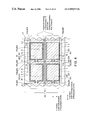
- FIG. 1 is a perspective view of a liquid crystal display device.
- FIG. 2 is an exploded perspective view of a liquid crystal panel used in the liquid crystal display device shown in FIG. 1 .
- FIG. 3 is a plan view which shows the configuration pattern of transparent electrodes formed on a first substrate of the liquid crystal panel shown in FIG. 1 .
- FIG. 4 is a plan view which shows the configuration pattern of transparent electrodes formed on a second substrate of the liquid crystal panel shown in FIG. 1 .
- FIGS. 5(A) and 5(B) are a sectional view of the liquid crystal panel shown in FIG. 1 and an enlarged sectional view of the end thereof, respectively.
- FIG. 6 is a plan view of the liquid crystal panel shown in FIG. 1 , schematically showing the relationship between the regions for forming alignment layers and the regions for forming a sealant.
- FIG. 7 is a schematic diagram which shows first and second large substrates for forming a plurality of first and second substrates, respectively, regions for forming transparent insulation films and alignment layers (regions marked by broken lines slanting to the left) formed on the first and second large substrates, and regions for forming the sealant (regions marked by solid lines slanting to the right) in the fabrication process of the liquid crystal panel shown in FIG. 1 .
- FIG. 8 is a schematic diagram which shows first and second large substrates for forming a plurality of first and second substrates, respectively, regions for forming transparent insulation films and alignment layers (regions marked by broken lines slanting to the left) formed on the first and second large substrates, and regions for forming the sealant (regions marked by solid lines slanting to the right) in the fabrication process of a liquid crystal panel in accordance with a second embodiment of the present invention.
- FIG. 9 is a schematic diagram which shows first and second large substrates for forming a plurality of first and second substrates, respectively, regions for forming transparent insulation films and alignment layers (regions marked by broken lines slanting to the left) formed on the first and second large substrates, and regions for forming the sealant (regions marked by solid lines slanting to the right) in the fabrication process of a liquid crystal panel in accordance with a third embodiment of the present invention.
- FIG. 10 is a schematic diagram which shows first and second large substrates for forming a plurality of first and second substrates, respectively, regions for forming transparent insulation films and alignment layers (regions marked by broken lines slanting to the left) formed on the first and second large substrates, and regions for forming the sealant (regions marked by solid lines slanting to the right) in the fabrication process of a liquid crystal panel in accordance with a fourth embodiment of the present invention.
- FIGS. 11(A) and 11(B) are a sectional view of a conventional liquid crystal panel and an enlarged sectional view of the end thereof, respectively.
- FIG. 12 is a schematic diagram which shows first and second large substrates for forming a plurality of first and second substrates, respectively, regions for forming transparent insulation films and alignment layers (regions marked by lines slanting to the left) formed on the first and second large substrates, and regions for forming the sealant (regions marked by lines slanting to the right) in the fabrication process of the conventional liquid crystal panel shown in FIGS. 11(A) and 11(B) .
- FIG. 1 is a perspective view of a liquid crystal display device and FIG. 2 is an exploded perspective view thereof.
- FIGS. 1 and 2 only portions of wiring patterns and terminals are shown, and the details thereof are shown in FIGS. 3 and 4 .
- a liquid crystal panel 10 of a liquid crystal display device mounted on an electronic apparatus such as a cordless telephone includes a first substrate 1 composed of transparent glass or the like and a second substrate 2 also composed of transparent glass or the like.
- a sealant 3 containing gap fillers and conductive particles is formed on one of the substrates by printing or the like, and the first substrate 1 and the second substrate 2 are bonded to each other with the sealant 3 therebetween.
- a predetermined gap is maintained between the first substrate 1 and the second substrate 2 by the gap fillers contained in the sealant 3 , and a liquid crystal 40 is enclosed in the gap in a liquid crystal filling-region 41 which is delimited by the sealant 3 .
- a polarizer 4 A is attached to the outer surface of the first substrate 1 by an adhesive or the like, and a polarizer 4 B is attached to the outer surface of the second substrate 2 by an adhesive or the like.
- a reflector (not shown in the drawing) is attached to the exterior of the polarizer 4 B attached to the second substrate 2 or is attached instead of the polarizer 4 B.
- the second substrate 2 is larger than the first substrate 1 , when the first substrate 1 is overlaid on the second substrate 2 , a portion of the second substrate 2 protrudes from the lower edge of the first substrate 1 .
- an IC mounting region 9 is formed, and a driver IC 33 is mounted thereon by a COG (Chip On Glass) method.
- a plurality of input-output terminals 7 D are formed along the edge of the substrate so as to adjoin the IC mounting region 9 on the lower edge side of the IC mounting region 9 .
- a flexible substrate 29 is connected to the input-output terminals 7 D, as shown by two-dot chain lines in FIG. 1 .
- FIGS. 3 and 4 are plan views which show the configuration patterns of transparent electrodes formed on the first substrate 1 and the second substrate 2 , respectively.
- an electrode pattern 6 which is provided with electrodes 6 A for displaying characters or for displaying dots and terminals 6 C for conducting between substrates lying along a side 101 in order to obtain conduction to the second substrate 2 in the exterior to the liquid crystal filling-region 41 , is formed on the inner surface of the first substrate 1 .
- the electrode pattern 6 is composed of an ITO film or the like.
- an electrode pattern 7 which is provided with electrodes 7 A for displaying characters or for displaying dots and a wiring section 7 B for wiring the electrodes 7 A toward the IC mounting region 9 in the exterior of the liquid crystal filling-region 41 , and terminals 7 C for conducting between substrates lying along a side 201 in order to obtain conduction to the first substrate 1 in the exterior of the liquid crystal filling-region 41 , is formed.
- the electrode pattern 7 is also composed of an ITO film or the like.
- the conductive particles contained in the sealant 3 interposed between the terminals 6 C and 7 C electrically connect the terminals 6 C and 7 C, and thus conduction between the first substrate 1 and the second substrate 2 is enabled. That is, the conductive particles contained in the sealant 3 are composed of elastically deformable plastic beads which are subjected to nickel plating or gold plating, and have particle sizes of approximately 5 to 9 ⁇ m.
- the gap fillers contained in the sealant 3 have particle sizes of approximately 4 to 8 ⁇ m. Therefore, when the sealant 3 is melted and cured while the first substrate 1 is superposed on the second substrate 2 and pressure is applied so as to narrow the gap, the conductive particles, in a squeezed state between the first substrate 1 and the second substrate 2 , electrically connect the terminals 6 C of the first substrate 1 to the terminal 7 C of the second substrate 2 .
- FIGS. 5(A) and 5(B) are a sectional view of the liquid crystal panel shown in FIG. 1 and an enlarged sectional view of the end thereof, respectively.
- FIG. 6 is a plan view of the liquid crystal panel shown in FIG. 1 , schematically showing the relationship between the regions for forming alignment layers and the regions for forming the sealant.
- the liquid crystal panel 10 having such a structure, as shown in FIGS. 5(A) and 5(B) , in the first substrate 1 and the second substrate 2 , transparent insulation films 12 and 22 are formed so as to cover the electrodes 6 A and 7 A, and on the surface of the transparent insulation films 12 and 22 , alignment layers 13 and 23 composed of polyimide films are formed.
- the alignment layers 13 and 23 are the polyimide films which are subjected to rubbing treatment, and the liquid crystal 40 is used in STN (Super Twisted Nematic) mode.
- the regions for forming alignment layers 13 and 23 and transparent insulation films 12 and 22 are shown by slanted broken lines, and the regions for forming the sealant 3 are shown by slanted solid lines
- the transparent insulation films 12 and 22 and the alignment layers 13 and 23 are formed up to the region overlapping the region for forming the sealant 3 in the sections corresponding to four sides 101 to 104 and 201 to 204 of the first and second substrates 1 and 2 , respectively.
- a one-part thermosetting epoxy sealant which has good adhesion even to polyimide films constituting the alignment layers 13 and 23 .
- Structbond ES series (trade name) manufactured by Mitsui Toatsu Kagaku K. K. is used.
- a latent curing agent such as dicyandiamide, a dihydrazide, or an imidazole, is dispersed in an epoxy resin, and an inorganic filler, a solvent, a viscosity modifier, etc. are further mixed thereto.
- thermosetting epoxy sealants since the Structbond ES series manufactured by Mitsui Toatsu Kagaku K. K. has excellent adhesion even to polyimide films, even if the sealant 3 is formed so as to overlap the surface of the alignment layers 13 and 23 , excellent water-tightness and airtightness are demonstrated at the interfaces.
- terminals 6 C for conducting to the second substrate 2 are formed in the section corresponding to the side 101 of the first substrate 1
- terminals 7 C for conducting to the first substrate 1 and the input-output terminals 7 D are formed in the section corresponding to the side 201 of the second substrate 2 , if the terminals 6 C, 7 C, and 7 D are covered with the alignment layers 13 and 23 , electrical continuity cannot be obtained.
- the alignment layers 13 and 23 are formed so as to partially overlap the regions for forming the sealant 3 , and in the sections corresponding to the other three sides 102 to 104 and 202 to 204 , the alignment layers 13 and 23 are formed up to the edges of the first and second substrates 1 and 2 .
- the transparent insulation films 12 and 22 which are formed so as to cover the electrodes 6 C and 7 C, are formed so as to substantially overlap the alignment layers 13 and 23 . That is, with respect to the transparent insulation films 12 and 22 , if the terminals 6 C and 7 C for conduction and the input-output terminals 7 D of the first and second substrates 1 and 2 are covered, electrical continuity cannot be obtained.
- the transparent insulation films 12 and 22 are formed so as to partially overlap the regions for forming the sealant 3 , and in the sections corresponding to the other three sides 102 to 104 and 202 to 204 , the transparent insulation films 12 and 22 are formed up to the edges of the first and second substrates 1 and 2 .
- FIG. 7 is a schematic diagram which shows the first and second large substrates 1 A and 2 A for forming a plurality of first and second substrates 1 and 2 , respectively, regions for forming the transparent insulation films 12 and 22 and the alignment layers 13 and 23 formed on the first and second large substrates 1 A and 2 A, and regions for forming the sealant 3 in the fabrication process of the liquid crystal panel shown in FIG. 1 .
- FIG. 7 is a schematic diagram which shows the first and second large substrates 1 A and 2 A for forming a plurality of first and second substrates 1 and 2 , respectively, regions for forming the transparent insulation films 12 and 22 and the alignment layers 13 and 23 formed on the first and second large substrates 1 A and 2 A, and regions for forming the sealant 3 in the fabrication process of the liquid crystal panel shown in FIG. 1 .
- FIG. 7 is a schematic diagram which shows the first and second large substrates 1 A and 2 A for forming a plurality of first and second substrates 1 and 2 , respectively, regions for forming the transparent insulation films
- first and second large substrates 1 A and 2 A for forming a plurality of first and second substrates 1 and 2 respectively, regions for forming the transparent insulation films 12 and 22 and the alignment layers 13 and 23 (regions marked by slanted broken lines) in relation to the first and second large substrates 1 A and 2 A, and regions for forming the sealant 3 (regions marked by slanted solid lines) are shown and other components are omitted, the individual components to be formed on the first and second large substrates 1 A and 2 A will be described with reference to FIGS. 5(A) and 5(B) .
- electrode patterns 6 and 7 including the electrodes 6 A and 7 A and the terminals 6 C and 7 C are formed by photolithography in the individual substrate forming-regions, which are to be separated into the first and second substrates 1 and 2 by cutting the large substrates 1 A and 2 A along the cutting projection lines L 1 and L 2 .
- transparent insulation films 12 and 22 composed of silicon oxide films are formed so as to cover the electrodes 6 A and 7 A.
- the transparent insulation films 12 and 22 are formed in strip covering a plurality of substrate forming-regions including the cutting projection lines L 1 and L 2 . That is, in the first and second large substrates 1 A and 2 A, the substrate forming-regions are disposed with the cutting projection line L 2 therebetween so that the sides 101 and 201 , in which the input-output terminals 7 D and the terminals 6 C and 7 C for conducting between substrates are formed, are directed in the opposite directions, the transparent insulation films 12 and 22 are formed in strip along the cutting projection line L 2 .
- the transparent insulation films 12 and 22 are formed so as to be superposed on the regions for forming the sealant 3 .
- the transparent insulation films 12 and 22 are formed up to the edges of the first and second substrates 1 and 2 across the regions for forming the sealant 3 , and in the sections corresponding to the sides 101 and 201 in which the terminals 6 A and 7 A for conducting between substrates and the input-output terminals 7 D are formed, the transparent insulation films 12 and 22 are formed so as to partially overlap the regions for forming the sealant 3 .
- polyimide films are formed by flexographic printing so as to cover the transparent insulation films 12 and 22 in the first and second large substrates 1 A and 2 A.
- the polyimide films (alignment layers 13 and 23 ) are also formed in strip over the plurality of substrate forming-regions including the cutting projection lines L 1 and L 2 .
- the polyimide films are formed in strip along the cutting projection line L 2 by moving a roller in a flexographic printer along the cutting projection line L 2 with the end of the roller being directed toward the sides 101 and 201 .
- the polyimide films (alignment layers 13 and 23 ) are formed so as to be superposed on the regions for forming the sealant 3 .
- the polyimide films are formed up to the edges of the first and second substrates 1 and 2 across the regions for forming the sealant 3 and in the sections corresponding to the sides 101 and 201 in which the terminals 6 A and 7 A for conducting between substrates and the input-output terminals 7 D are formed, the polyimide films (alignment layers 13 and 23 ) are formed so as to partially overlap the regions for forming the sealant 3 .
- rubbing treatment is performed on the first and second large substrates to form the alignment layers 13 and 23 from the polyimide films.
- the bonded first large substrate 1 A and second large substrate 2 A are divided into single liquid crystal panels 10 by cutting along the cutting projection lines L 1 and L 2 , or the bonded first large substrate 1 A and second large substrate 2 A are divided into strip panels by cutting along the cutting projection line L 1 .
- openings 30 of the sealant 3 are opened in the cut surfaces (corresponding to the sides 104 and 204 ).
- the polarizers 4 A and 4 B, etc. are attached thereto.
- the strip panels are separated, after dividing the strip panels into single liquid crystal panels 10 , the polarizers 4 A and 4 B, etc. are attached thereto.
- the flexible substrate 29 is pressed onto the input-output terminals 7 D of the second substrate 2 using an anisotropic conductive film or the like, and is delivered to the inspection step.
- FIG. 8 is a schematic diagram which shows first and second large substrates for forming a plurality of first and second substrates, respectively, regions for forming transparent insulation films and alignment layers (regions marked by broken lines slanting to the left) formed on the first and second large substrates, and regions for forming the sealant (regions marked by solid lines slanting to the right) in the fabrication process of a liquid crystal panel in accordance with a second embodiment of the present invention. Since the basic structure of the liquid crystal panel in this embodiment is in common with that of the liquid crystal panel in accordance with the first embodiment, the same numerals are used for the corresponding sections in FIG. 8 , and the detailed description thereof will be omitted.
- transparent insulation films 12 and 22 composed of silicon oxide films are formed on first and second large substrates 1 A and 2 A so as to cover electrodes 6 A and 7 A (refer to FIGS. 3 , 4 , 5 (A), and 5 (B)).
- the transparent insulation films 12 and 22 cover a cutting projection line L 1 between cutting projection lines L 1 and L 2 , they do not cover the cutting projection line L 2 , and the transparent insulation films 12 and 22 are formed in strip by each row, covering a plurality of substrate forming-regions.
- the transparent insulation films 12 and 22 are formed so as to be superposed on the regions for forming the sealant 3 .
- the transparent insulation films 12 and 22 are formed up to the edges of the first and second substrates 1 and 2 across the regions for forming the sealant 3 .
- polyimide films (alignment layers 13 and 23 ) are formed by flexographic printing so as to cover the transparent insulation films 12 and 22 in the first and second large substrates 1 A and 2 A.
- the polyimide films also cover the cutting projection line L 1 between the cutting projection lines L 1 and L 2 and the polyimide films do not cover the cutting projection line L 2 .
- the polyimide films are formed in strip by each row over a plurality of substrate forming-regions.
- the polyimide films (alignment layers 13 and 23 ) are formed so as to be superposed on the regions for forming the sealant 3 .
- the polyimide films are formed up to the edges of the first and second substrates 1 and 2 across the regions for forming the sealant 3 .
- FIG. 9 is a schematic diagram which shows first and second large substrates for forming a plurality of first and second substrates, respectively, regions for forming transparent insulation films and alignment layers (regions marked by broken lines slanting to the left) formed on the first and second large substrates, and regions for forming the sealant (regions marked by solid lines slanting to the right) in the fabrication process of a liquid crystal panel in accordance with a third embodiment of the present invention. Since the basic structure of the liquid crystal panel in this embodiment is in common with that of the liquid crystal panel in accordance with the first embodiment, the same numerals are used for the corresponding sections in FIG. 9 , and the detailed description thereof will be omitted.
- transparent insulation films 12 and 22 composed of silicon oxide films are formed on first and second large substrates 1 A and 2 A so as to cover electrodes 6 A and 7 A (refer to FIGS. 3 , 4 , 5 (A), and 5 (B)).
- the transparent insulation films 12 and 22 cover a cutting projection line L 2 between cutting projection lines L 1 and L 2 , they do not cover the cutting projection line L 1 , and the transparent insulation films 12 and 22 are formed in strip, covering a plurality of substrate forming-regions.
- the transparent insulation films 12 and 22 are formed so as to be superposed on the regions for forming the sealant 3 .
- the transparent insulation films 12 and 22 are formed up to the edges of the first and second substrates 1 and 2 across the regions for forming the sealant 3 .
- Polyimide films are formed by flexographic printing so as to cover the transparent insulation films 12 and 22 in the first and second large substrates 1 A and 2 A.
- the polyimide films (alignment layers 13 and 23 ) also cover the cutting projection line L 2 between the cutting projection lines L 1 and L 2 and the polyimide films do not cover the cutting projection line L 1 .
- the polyimide films are formed in strip over a plurality of substrate forming-regions.
- the polyimide films (alignment layers 13 and 23 ) are formed so as to be superposed on the regions for forming the sealant 3 .
- the polyimide films are formed up to the edges of the first and second substrates 1 and 2 across the regions for forming the sealant 3 .
- FIG. 10 is a schematic diagram which shows first and second large substrates for forming a plurality of first and second substrates, respectively, regions for forming transparent insulation films and alignment layers (regions marked by broken lines slanting to the left) formed on the first and second large substrates, and regions for forming the sealant (regions marked by solid lines slanting to the right) in the fabrication process of a liquid crystal panel in accordance with a fourth embodiment of the present invention. Since the basic structure of the liquid crystal panel in this embodiment is in common with that of the liquid crystal panel in accordance with the first embodiment, the same numerals are used for the corresponding sections in FIG. 10 , and the detailed description thereof will be omitted.
- transparent insulation films 12 and 22 composed of silicon oxide films are formed on first and second large substrates 1 A and 2 A so as to cover electrodes 6 A and 7 A (refer to FIGS. 3 , 4 , 5 (A), and 5 (B)).
- the transparent insulation films 12 and 22 do not cover cutting projection lines L 1 and L 2 , and are formed independently by each substrate forming-region.
- the transparent insulation films 12 and 22 are formed so as to be superposed on the regions for forming the sealant 3 .
- Polyimide films are formed by flexographic printing so as to cover the transparent insulation films 12 and 22 in the first and second large substrates 1 A and 2 A.
- the polyimide films (alignment layers 13 and 23 ) do not cover the cutting projection lines L 1 and L 2 , and are formed independently by each substrate forming-region.
- first and second large substrates 1 A and 2 A are divided into single first and second substrates 1 and 2 by cutting along the cutting projection lines L 1 and L 2 , in the sections corresponding to the four sides 101 to 104 and 201 to 204 of the first and second substrates 1 and 2 , the polyimide films (alignment layers 13 and 23 ) are formed so as to be superposed on the regions for forming the sealant 3 .
- the transparent insulation films 12 and 22 and the polyimide films are formed so as to be superposed on the regions for forming the sealant 3 at the four sides of the substrate
- the transparent insulation films 12 and 22 and the polyimide films may be superposed on the regions for forming the sealant 3 at least at the three sides of the substrate.
- the regions for forming the transparent insulation films 12 and 22 and the polyimide films may be formed in the interior of the regions for forming the sealant 3 at the sides 101 and 201 in which terminals 6 A and 7 A for conducting between substrates and input-output terminals 7 D are formed, among the four sides 101 to 104 and 201 to 204 of the first and second substrates 1 and 2 .
- alignment layers, etc. are formed in the stage of large substrates, and after the large substrates are bonded to each other, they are divided into single liquid crystal panels, the present invention is also applicable to the case in which electrodes, alignment layers, etc. are formed on single substrates.
- the present invention is useful for liquid crystal display devices which require wider regions for displaying images and methods of fabricating the same, and in particular, the invention is suitable for a liquid crystal display device in which a larger amount of displaying is required by effectively using the limited region for displaying images.
Landscapes
- Physics & Mathematics (AREA)
- Nonlinear Science (AREA)
- General Physics & Mathematics (AREA)
- Optics & Photonics (AREA)
- Mathematical Physics (AREA)
- Chemical & Material Sciences (AREA)
- Crystallography & Structural Chemistry (AREA)
- Spectroscopy & Molecular Physics (AREA)
- Liquid Crystal (AREA)
Abstract
Description
Claims (25)
Applications Claiming Priority (3)
| Application Number | Priority Date | Filing Date | Title |
|---|---|---|---|
| JP24603298 | 1998-08-31 | ||
| JP10-246032 | 1998-08-31 | ||
| PCT/JP1999/004364 WO2000013059A1 (en) | 1998-08-31 | 1999-08-11 | Liquid crystal panel and method of manufacture thereof |
Publications (1)
| Publication Number | Publication Date |
|---|---|
| US6989879B1 true US6989879B1 (en) | 2006-01-24 |
Family
ID=17142446
Family Applications (1)
| Application Number | Title | Priority Date | Filing Date |
|---|---|---|---|
| US09/530,122 Expired - Lifetime US6989879B1 (en) | 1998-08-31 | 1999-08-11 | Liquid crystal panel and method of fabricating the same |
Country Status (6)
| Country | Link |
|---|---|
| US (1) | US6989879B1 (en) |
| JP (1) | JP3503597B2 (en) |
| KR (1) | KR100516656B1 (en) |
| CN (1) | CN1179237C (en) |
| TW (1) | TW498176B (en) |
| WO (1) | WO2000013059A1 (en) |
Cited By (17)
| Publication number | Priority date | Publication date | Assignee | Title |
|---|---|---|---|---|
| US20050073637A1 (en) * | 2003-10-01 | 2005-04-07 | Bing-Jei Liao | Liquid crystal display panel |
| US20050168676A1 (en) * | 2002-02-20 | 2005-08-04 | Fujitsu Display Technologies Corporation | Liquid crystal display device's substrate, liquid crystal display device including the same, and manufacturing method of the same |
| US20050280765A1 (en) * | 2004-06-18 | 2005-12-22 | Innolux Display Corp. | Liquid crystal display panel and method for manufacturing the same |
| US20060077334A1 (en) * | 2004-08-27 | 2006-04-13 | Seong-Ho Kim | Displaying apparatus |
| US20070085952A1 (en) * | 2003-06-04 | 2007-04-19 | Masateru Morimoto | Display device and manufacturing method thereof |
| US20070224369A1 (en) * | 2006-03-24 | 2007-09-27 | Seiko Epson Corporation | Liquid crystal device, method for manufacturing the same, and electronic apparatus |
| US20080011802A1 (en) * | 2006-07-14 | 2008-01-17 | Innolux Display Corp. | Cutting system for master liquid crystal panel having different alignment marks and method for cutting master liquid crystal panel |
| US20110228207A1 (en) * | 2010-03-22 | 2011-09-22 | Samsung Mobile Display Co., Ltd. | Liquid crystal display device and method of manufacturing the same |
| US20110242472A1 (en) * | 2010-04-02 | 2011-10-06 | Seiko Epson Corporation | Electrooptic device and electronic apparatus |
| US20120075559A1 (en) * | 2010-09-28 | 2012-03-29 | Panasonic Liquid Crystal Display Co., Ltd. | Liquid crystal display device |
| US20130314783A1 (en) * | 2012-05-23 | 2013-11-28 | Lg Display Co., Ltd. | Polarization film having black strip for applying to a patterned retarder type 3d display device |
| US20140071388A1 (en) * | 2012-03-22 | 2014-03-13 | Shenzhen China Star Optoelectronics Technology Co., Ltd. | Liquid crystal display device and manufacturing method thereof |
| US20150092148A1 (en) * | 2013-10-01 | 2015-04-02 | Japan Display Inc. | Liquid crystal display device |
| US20150109569A1 (en) * | 2013-10-22 | 2015-04-23 | Japan Display Inc. | Liquid crystal display device |
| US10216045B2 (en) | 2014-12-10 | 2019-02-26 | Lg Display Co., Ltd. | Liquid crystal display device and display apparatus |
| EP3422089A4 (en) * | 2016-02-22 | 2019-09-04 | Dai Nippon Printing Co., Ltd. | Light control cell |
| US11333940B2 (en) * | 2012-10-01 | 2022-05-17 | Japan Display Inc. | Display device and manufacturing method thereof |
Families Citing this family (7)
| Publication number | Priority date | Publication date | Assignee | Title |
|---|---|---|---|---|
| KR100790352B1 (en) * | 2001-05-22 | 2008-01-02 | 엘지.필립스 엘시디 주식회사 | Reflective and transflective liquid crystal display devices and manufacturing methods thereof |
| JP4064687B2 (en) * | 2002-02-20 | 2008-03-19 | シャープ株式会社 | Liquid crystal display device and manufacturing method thereof |
| KR101007715B1 (en) * | 2003-09-19 | 2011-01-13 | 삼성전자주식회사 | Liquid Crystal Display and Manufacturing Method Thereof |
| KR101100892B1 (en) * | 2004-08-27 | 2012-01-02 | 삼성전자주식회사 | Display device |
| JP4631923B2 (en) * | 2008-04-11 | 2011-02-16 | ソニー株式会社 | Liquid crystal device and electronic device |
| CN103576390A (en) * | 2012-08-01 | 2014-02-12 | 立景光电股份有限公司 | monitor |
| CN110187566A (en) * | 2019-05-10 | 2019-08-30 | 深圳市华星光电技术有限公司 | Frame glue and liquid crystal display panel |
Citations (32)
| Publication number | Priority date | Publication date | Assignee | Title |
|---|---|---|---|---|
| JPS5238948A (en) | 1975-09-23 | 1977-03-25 | Sharp Corp | Liquid crystal cell for display |
| US4391491A (en) * | 1979-05-04 | 1983-07-05 | Ebauches Electroniques, S.A. | Passive electro-optic display cell and method of manufacturing thereof |
| JPS59174820A (en) * | 1983-03-24 | 1984-10-03 | Sharp Corp | Liquid crystal display element |
| JPS60181730A (en) * | 1984-02-29 | 1985-09-17 | Toshiba Corp | Liquid crystal display device |
| JPS60181731A (en) | 1984-02-29 | 1985-09-17 | Hitachi Ltd | Liquid-crystal display element |
| JPS62269119A (en) * | 1986-05-16 | 1987-11-21 | Stanley Electric Co Ltd | Liquid crystal display element |
| JPS62269934A (en) | 1986-05-19 | 1987-11-24 | Stanley Electric Co Ltd | Manufacturing method of liquid crystal display element |
| US4759614A (en) * | 1985-07-10 | 1988-07-26 | Hitachi, Ltd. | Ferroelectric liquid crystal element with particular alignment film and a method for manufacturing the same |
| EP0466112A2 (en) * | 1990-07-12 | 1992-01-15 | Seiko Epson Corporation | Electrooptic device |
| JPH0477131A (en) | 1990-07-17 | 1992-03-11 | Kemikaraijingu Kenkyusho:Kk | Optical transmitter-receiver |
| US5150239A (en) * | 1990-02-09 | 1992-09-22 | Canon Kabushiki Kaisha | One-pack type epoxy sealant with amine-type curing agent, for liquid crystal cell, display apparatus and recording apparatus |
| KR940015614A (en) | 1992-12-28 | 1994-07-21 | 석진철 | Manufacturing method of liquid crystal panel |
| JPH06208124A (en) | 1993-01-11 | 1994-07-26 | Hitachi Ltd | Liquid crystal display element |
| US5396355A (en) * | 1991-06-17 | 1995-03-07 | Seiko Epson Corporation | Optically compensating film, optical compensator and liquid crystal display |
| JPH08278489A (en) | 1995-04-07 | 1996-10-22 | Citizen Watch Co Ltd | Production of liquid crystal display panel |
| US5625473A (en) * | 1993-05-06 | 1997-04-29 | Sharp Kabushiki Kaisha | Liquid crystal display device with polymer walls and method for producing the same |
| US5717474A (en) * | 1994-09-30 | 1998-02-10 | Honeywell Inc. | Wide-viewing angle multi-domain halftone active matrix liquid crystal display having compensating retardation |
| JPH10198285A (en) | 1997-01-13 | 1998-07-31 | Toshiba Corp | Flat panel display |
| US5818625A (en) * | 1997-04-02 | 1998-10-06 | Gentex Corporation | Electrochromic rearview mirror incorporating a third surface metal reflector |
| US5959713A (en) * | 1996-10-04 | 1999-09-28 | Seiko Epson Corporation | Liquid-crystal display panel and method for inspecting the same |
| US6052170A (en) * | 1997-05-13 | 2000-04-18 | Seiko Epson Corporation | Inspectable liquid-crystal display panel and method of inspecting same |
| US6144431A (en) * | 1996-10-17 | 2000-11-07 | Sharp Kabushiki Kaisha | Liquid crystal display device having at least one phase-different plate between LC element and a polarizer wherein the principal refractive indices of said phase-different plate satisfies na=nc>nb |
| US6151091A (en) * | 1997-12-25 | 2000-11-21 | Seiko Epson Corporation | Liquid crystal display device including film |
| US6172727B1 (en) * | 1997-03-31 | 2001-01-09 | Denso Corporation | Liquid crystal cell having alignment films rubbed with differing rubbing densities |
| US6226067B1 (en) * | 1997-10-03 | 2001-05-01 | Minolta Co., Ltd. | Liquid crystal device having spacers and manufacturing method thereof |
| US6327012B1 (en) * | 1997-12-22 | 2001-12-04 | Sharp Kabushiki Kaisha | Method for manufacturing liquid crystal display |
| US6335773B1 (en) * | 1997-12-22 | 2002-01-01 | Hitachi Ltd | Liquid crystal display device in which the light length, polarizing axis, and alignment direction are related |
| US20020001056A1 (en) * | 2000-04-05 | 2002-01-03 | Edmund Sandberg | Reflective microdisplay for light engine based video projection applictions |
| US6400438B1 (en) * | 1997-04-04 | 2002-06-04 | Sanyo Electric Co., Ltd. | Glass board used in the production of liquid crystal panels |
| US6459467B1 (en) * | 1998-05-15 | 2002-10-01 | Minolta Co., Ltd. | Liquid crystal light modulating device, and a manufacturing method and a manufacturing apparatus thereof |
| US6507381B1 (en) * | 1997-05-26 | 2003-01-14 | Sharp Kabushiki Kaisha | Liquid crystal panel having tilted liquid crystal molecules and liquid crystal display using the liquid crystal panel |
| US6515729B1 (en) * | 1998-07-29 | 2003-02-04 | Citizen Watch Co., Ltd. | Reflection-type color liquid crystal display device |
-
1999
- 1999-08-11 CN CNB998014524A patent/CN1179237C/en not_active Expired - Lifetime
- 1999-08-11 JP JP2000567986A patent/JP3503597B2/en not_active Expired - Lifetime
- 1999-08-11 WO PCT/JP1999/004364 patent/WO2000013059A1/en not_active Ceased
- 1999-08-11 KR KR10-2000-7004531A patent/KR100516656B1/en not_active Expired - Lifetime
- 1999-08-11 US US09/530,122 patent/US6989879B1/en not_active Expired - Lifetime
- 1999-08-27 TW TW088114750A patent/TW498176B/en not_active IP Right Cessation
Patent Citations (34)
| Publication number | Priority date | Publication date | Assignee | Title |
|---|---|---|---|---|
| JPS5238948A (en) | 1975-09-23 | 1977-03-25 | Sharp Corp | Liquid crystal cell for display |
| US4391491A (en) * | 1979-05-04 | 1983-07-05 | Ebauches Electroniques, S.A. | Passive electro-optic display cell and method of manufacturing thereof |
| JPS59174820A (en) * | 1983-03-24 | 1984-10-03 | Sharp Corp | Liquid crystal display element |
| JPS60181730A (en) * | 1984-02-29 | 1985-09-17 | Toshiba Corp | Liquid crystal display device |
| JPS60181731A (en) | 1984-02-29 | 1985-09-17 | Hitachi Ltd | Liquid-crystal display element |
| US4759614A (en) * | 1985-07-10 | 1988-07-26 | Hitachi, Ltd. | Ferroelectric liquid crystal element with particular alignment film and a method for manufacturing the same |
| JPS62269119A (en) * | 1986-05-16 | 1987-11-21 | Stanley Electric Co Ltd | Liquid crystal display element |
| JPS62269934A (en) | 1986-05-19 | 1987-11-24 | Stanley Electric Co Ltd | Manufacturing method of liquid crystal display element |
| US5150239A (en) * | 1990-02-09 | 1992-09-22 | Canon Kabushiki Kaisha | One-pack type epoxy sealant with amine-type curing agent, for liquid crystal cell, display apparatus and recording apparatus |
| EP0466112A2 (en) * | 1990-07-12 | 1992-01-15 | Seiko Epson Corporation | Electrooptic device |
| JPH0470811A (en) | 1990-07-12 | 1992-03-05 | Seiko Epson Corp | Electro-optical device and method for manufacturing electro-optical device |
| US5317434A (en) * | 1990-07-12 | 1994-05-31 | Seiko Epson Corporation | Color filter structure for liquid crystal displays with seal end on or surrounded by orientation film |
| JPH0477131A (en) | 1990-07-17 | 1992-03-11 | Kemikaraijingu Kenkyusho:Kk | Optical transmitter-receiver |
| US5396355A (en) * | 1991-06-17 | 1995-03-07 | Seiko Epson Corporation | Optically compensating film, optical compensator and liquid crystal display |
| KR940015614A (en) | 1992-12-28 | 1994-07-21 | 석진철 | Manufacturing method of liquid crystal panel |
| JPH06208124A (en) | 1993-01-11 | 1994-07-26 | Hitachi Ltd | Liquid crystal display element |
| US5625473A (en) * | 1993-05-06 | 1997-04-29 | Sharp Kabushiki Kaisha | Liquid crystal display device with polymer walls and method for producing the same |
| US5717474A (en) * | 1994-09-30 | 1998-02-10 | Honeywell Inc. | Wide-viewing angle multi-domain halftone active matrix liquid crystal display having compensating retardation |
| JPH08278489A (en) | 1995-04-07 | 1996-10-22 | Citizen Watch Co Ltd | Production of liquid crystal display panel |
| US5959713A (en) * | 1996-10-04 | 1999-09-28 | Seiko Epson Corporation | Liquid-crystal display panel and method for inspecting the same |
| US6144431A (en) * | 1996-10-17 | 2000-11-07 | Sharp Kabushiki Kaisha | Liquid crystal display device having at least one phase-different plate between LC element and a polarizer wherein the principal refractive indices of said phase-different plate satisfies na=nc>nb |
| JPH10198285A (en) | 1997-01-13 | 1998-07-31 | Toshiba Corp | Flat panel display |
| US6172727B1 (en) * | 1997-03-31 | 2001-01-09 | Denso Corporation | Liquid crystal cell having alignment films rubbed with differing rubbing densities |
| US5818625A (en) * | 1997-04-02 | 1998-10-06 | Gentex Corporation | Electrochromic rearview mirror incorporating a third surface metal reflector |
| US6400438B1 (en) * | 1997-04-04 | 2002-06-04 | Sanyo Electric Co., Ltd. | Glass board used in the production of liquid crystal panels |
| US6052170A (en) * | 1997-05-13 | 2000-04-18 | Seiko Epson Corporation | Inspectable liquid-crystal display panel and method of inspecting same |
| US6507381B1 (en) * | 1997-05-26 | 2003-01-14 | Sharp Kabushiki Kaisha | Liquid crystal panel having tilted liquid crystal molecules and liquid crystal display using the liquid crystal panel |
| US6226067B1 (en) * | 1997-10-03 | 2001-05-01 | Minolta Co., Ltd. | Liquid crystal device having spacers and manufacturing method thereof |
| US6327012B1 (en) * | 1997-12-22 | 2001-12-04 | Sharp Kabushiki Kaisha | Method for manufacturing liquid crystal display |
| US6335773B1 (en) * | 1997-12-22 | 2002-01-01 | Hitachi Ltd | Liquid crystal display device in which the light length, polarizing axis, and alignment direction are related |
| US6151091A (en) * | 1997-12-25 | 2000-11-21 | Seiko Epson Corporation | Liquid crystal display device including film |
| US6459467B1 (en) * | 1998-05-15 | 2002-10-01 | Minolta Co., Ltd. | Liquid crystal light modulating device, and a manufacturing method and a manufacturing apparatus thereof |
| US6515729B1 (en) * | 1998-07-29 | 2003-02-04 | Citizen Watch Co., Ltd. | Reflection-type color liquid crystal display device |
| US20020001056A1 (en) * | 2000-04-05 | 2002-01-03 | Edmund Sandberg | Reflective microdisplay for light engine based video projection applictions |
Non-Patent Citations (5)
| Title |
|---|
| Communication from Japanese Patent Office re: counterpart application. |
| Communication from Korean Patent Office re: counterpart application. |
| Correspondence from Japanese Patent Office regarding counterpart application. |
| Japanese Search Report for 2000-567986. |
| Republic of China First Office Action, China Application No. 99801452.4. |
Cited By (57)
| Publication number | Priority date | Publication date | Assignee | Title |
|---|---|---|---|---|
| US20080106687A1 (en) * | 2002-02-20 | 2008-05-08 | Sharp Kabushiki Kaisha | Liquid crystal display device's substrate, liquid crystal display device including the same, and manufacturing method of the same |
| US20050168676A1 (en) * | 2002-02-20 | 2005-08-04 | Fujitsu Display Technologies Corporation | Liquid crystal display device's substrate, liquid crystal display device including the same, and manufacturing method of the same |
| US8004640B2 (en) | 2002-02-20 | 2011-08-23 | Sharp Kabushiki Kaisha | Liquid crystal display device |
| US8755009B2 (en) | 2002-02-20 | 2014-06-17 | Sharp Kabushiki Kaisha | Liquid crystal display device's substrate, liquid crystal display device including the same, and manufacturing method of the same |
| US7847900B2 (en) | 2002-02-20 | 2010-12-07 | Sharp Kabushiki Kaisha | Liquid crystal display device's substrate, liquid crystal display device including the same, and manufacturing method of the same |
| US20080106683A1 (en) * | 2002-02-20 | 2008-05-08 | Sharp Kabushiki Kaisha | Liquid crystal display device's substrate, liquid crystal display device including the same, and manufacturing method of the same |
| US8045124B2 (en) | 2002-02-20 | 2011-10-25 | Sharp Kabushiki Kaisha | Liquid crystal display device's substrate, liquid crystal display device including the same, and manufacturing method of the same |
| US20080062368A1 (en) * | 2002-02-20 | 2008-03-13 | Sharp Kabushiki Kaisha | Liquid crystal display device's substrate, liquid crystal display device including the same, and manufacturing method of the same |
| US7345719B2 (en) | 2002-02-20 | 2008-03-18 | Sharp Kabushiki Kaisha | Liquid crystal display device's substrate, liquid crystal display device including the same, and manufacturing method of the same |
| US20070085952A1 (en) * | 2003-06-04 | 2007-04-19 | Masateru Morimoto | Display device and manufacturing method thereof |
| US7751007B2 (en) | 2003-06-04 | 2010-07-06 | Hitachi Displays, Ltd. | Display device and manufacturing method thereof |
| US20050073637A1 (en) * | 2003-10-01 | 2005-04-07 | Bing-Jei Liao | Liquid crystal display panel |
| US20080192195A1 (en) * | 2003-10-01 | 2008-08-14 | Bing-Jei Liao | Liquid crystal display panel |
| US7433011B2 (en) * | 2003-10-01 | 2008-10-07 | Himax Technologies Limited | Liquid crystal display panel |
| US20100085519A1 (en) * | 2003-10-01 | 2010-04-08 | Bing-Jei Liao | Liquid crystal display panel |
| US7705942B2 (en) | 2003-10-01 | 2010-04-27 | Himax Technologies Limited | Liquid crystal display panel |
| US7443481B2 (en) * | 2004-06-18 | 2008-10-28 | Innolux Display Corp. | Method for manufacturing a LCD panel comprising applying an electrically conductive adhesive to an opening defined by a plate sealing adhesive and introducing liquid crystal material by a one drop fill method |
| US20050280765A1 (en) * | 2004-06-18 | 2005-12-22 | Innolux Display Corp. | Liquid crystal display panel and method for manufacturing the same |
| US7554637B2 (en) * | 2004-08-27 | 2009-06-30 | Samsung Electronics Co., Ltd. | Liquid crystal display panel and display apparatus having the same |
| US20060077334A1 (en) * | 2004-08-27 | 2006-04-13 | Seong-Ho Kim | Displaying apparatus |
| US20070224369A1 (en) * | 2006-03-24 | 2007-09-27 | Seiko Epson Corporation | Liquid crystal device, method for manufacturing the same, and electronic apparatus |
| US20080011802A1 (en) * | 2006-07-14 | 2008-01-17 | Innolux Display Corp. | Cutting system for master liquid crystal panel having different alignment marks and method for cutting master liquid crystal panel |
| US20110228207A1 (en) * | 2010-03-22 | 2011-09-22 | Samsung Mobile Display Co., Ltd. | Liquid crystal display device and method of manufacturing the same |
| US8537328B2 (en) | 2010-03-22 | 2013-09-17 | Samsung Display Co., Ltd. | Liquid crystal display device and method of manufacturing the same |
| US20110242472A1 (en) * | 2010-04-02 | 2011-10-06 | Seiko Epson Corporation | Electrooptic device and electronic apparatus |
| US8421969B2 (en) * | 2010-04-02 | 2013-04-16 | Seiko Epson Corporation | Electrooptic device and electronic apparatus |
| US9261735B2 (en) * | 2010-09-28 | 2016-02-16 | Japan Display Inc. | Liquid crystal display device |
| US20120075559A1 (en) * | 2010-09-28 | 2012-03-29 | Panasonic Liquid Crystal Display Co., Ltd. | Liquid crystal display device |
| US9715146B2 (en) | 2010-09-28 | 2017-07-25 | Japan Display Inc. | Liquid crystal display device |
| US20140071388A1 (en) * | 2012-03-22 | 2014-03-13 | Shenzhen China Star Optoelectronics Technology Co., Ltd. | Liquid crystal display device and manufacturing method thereof |
| US9541688B2 (en) * | 2012-05-23 | 2017-01-10 | Lg Display Co., Ltd. | Polarization film having black strip for applying to a patterned retarder type 3D display device |
| US20130314783A1 (en) * | 2012-05-23 | 2013-11-28 | Lg Display Co., Ltd. | Polarization film having black strip for applying to a patterned retarder type 3d display device |
| US11573464B2 (en) * | 2012-10-01 | 2023-02-07 | Japan Display Inc. | Display device and manufacturing method thereof |
| US11852932B2 (en) * | 2012-10-01 | 2023-12-26 | Japan Display Inc. | Display device and manufacturing method thereof |
| US12321069B2 (en) * | 2012-10-01 | 2025-06-03 | Japan Display Inc. | Display device and manufacturing method thereof |
| US20240369887A1 (en) * | 2012-10-01 | 2024-11-07 | Japan Display Inc. | Display device and manufacturing method thereof |
| US11333940B2 (en) * | 2012-10-01 | 2022-05-17 | Japan Display Inc. | Display device and manufacturing method thereof |
| US20230138640A1 (en) * | 2012-10-01 | 2023-05-04 | Japan Display Inc. | Display device and manufacturing method thereof |
| US20220236602A1 (en) * | 2012-10-01 | 2022-07-28 | Japan Display Inc. | Display device and manufacturing method thereof |
| US12078895B2 (en) * | 2012-10-01 | 2024-09-03 | Japan Display Inc. | Display device and manufacturing method thereof |
| US9933660B2 (en) * | 2013-10-01 | 2018-04-03 | Japan Display Inc. | Liquid crystal display device |
| US12001103B2 (en) | 2013-10-01 | 2024-06-04 | Japan Display Inc. | Liquid crystal display device with sealant in contact with inorganic alignment films |
| US12326634B2 (en) | 2013-10-01 | 2025-06-10 | Japan Display Inc. | Liquid crystal display device with sealant in contact with inorganic alignment films |
| US20160313582A1 (en) * | 2013-10-01 | 2016-10-27 | Japan Display Inc. | Liquid crystal display device |
| US9411201B2 (en) * | 2013-10-01 | 2016-08-09 | Japan Display Inc. | Liquid crystal display device |
| US20150092148A1 (en) * | 2013-10-01 | 2015-04-02 | Japan Display Inc. | Liquid crystal display device |
| US10948781B2 (en) * | 2013-10-01 | 2021-03-16 | Japan Display Inc. | Liquid crystal display device |
| US11281050B2 (en) | 2013-10-01 | 2022-03-22 | Japan Display Inc. | Liquid crystal display device |
| US10551679B2 (en) * | 2013-10-01 | 2020-02-04 | Japan Display Inc. | Liquid crystal display device |
| US11681183B2 (en) | 2013-10-01 | 2023-06-20 | Japan Display Inc. | Liquid crystal display device |
| US20150109569A1 (en) * | 2013-10-22 | 2015-04-23 | Japan Display Inc. | Liquid crystal display device |
| CN104570488A (en) * | 2013-10-22 | 2015-04-29 | 株式会社日本显示器 | Liquid crystal display device |
| CN104570488B (en) * | 2013-10-22 | 2018-04-13 | 株式会社日本显示器 | Liquid crystal display device |
| US10216045B2 (en) | 2014-12-10 | 2019-02-26 | Lg Display Co., Ltd. | Liquid crystal display device and display apparatus |
| US10788717B2 (en) | 2014-12-10 | 2020-09-29 | Lg Display Co., Ltd. | Liquid crystal display device and display apparatus |
| EP3422089A4 (en) * | 2016-02-22 | 2019-09-04 | Dai Nippon Printing Co., Ltd. | Light control cell |
| US10795212B2 (en) * | 2016-02-22 | 2020-10-06 | Dai Nippon Printing Co., Ltd. | Light-modulating cell |
Also Published As
| Publication number | Publication date |
|---|---|
| CN1275215A (en) | 2000-11-29 |
| CN1179237C (en) | 2004-12-08 |
| JP3503597B2 (en) | 2004-03-08 |
| KR100516656B1 (en) | 2005-09-22 |
| KR20010031494A (en) | 2001-04-16 |
| WO2000013059A1 (en) | 2000-03-09 |
| TW498176B (en) | 2002-08-11 |
Similar Documents
| Publication | Publication Date | Title |
|---|---|---|
| US6989879B1 (en) | Liquid crystal panel and method of fabricating the same | |
| US7164460B2 (en) | Mounting structure for semiconductor device, electro-optical device, and electronic apparatus | |
| CN100412665C (en) | Liquid crystal display device and manufacturing method thereof | |
| US6573957B1 (en) | Liquid crystal display device | |
| US5798812A (en) | Active matrix substrate and display device using the same with extending protrusions between gate and source line terminals | |
| KR100763408B1 (en) | Liquid crystal display | |
| US6724448B2 (en) | Liquid crystal display device and manufacturing method by compression bonding | |
| JPWO2000013059A1 (en) | Liquid crystal panel and its manufacturing method | |
| US20020018149A1 (en) | Liquid crystal display panel and method of manufactuing the same | |
| KR100389492B1 (en) | Liquid crystal device and its production method | |
| EP0871060A1 (en) | Liquid crystal display and electronics equipment using the same | |
| KR102348373B1 (en) | Liquid crystal display device | |
| JP4408192B2 (en) | Substrate for liquid crystal display device, liquid crystal display device including the same, and manufacturing method thereof | |
| US7675602B2 (en) | Board device and method for manufacturing display element | |
| US6741315B1 (en) | Liquid crystal device and electronic apparatus | |
| JP3695265B2 (en) | Display device and electronic device | |
| JP3636193B2 (en) | Liquid crystal panel and method of manufacturing liquid crystal panel | |
| JP2008216966A (en) | Manufacturing method of electrooptical device, electrooptical device, and electronic equipment | |
| JP2001083543A (en) | Liquid crystal display device | |
| JP2000284261A (en) | Liquid crystal devices and electronic equipment | |
| JP4474770B2 (en) | Electro-optical device and electronic apparatus | |
| JP4136119B2 (en) | LCD panel | |
| JPH11258618A (en) | Liquid crystal display element and its manufacture | |
| JP3567781B2 (en) | Liquid crystal device, method of manufacturing liquid crystal device, and electronic equipment | |
| JP2001125116A (en) | Liquid crystal panel and method of manufacturing the same |
Legal Events
| Date | Code | Title | Description |
|---|---|---|---|
| AS | Assignment |
Owner name: SEIKO EPSON CORPORATION, JAPAN Free format text: ASSIGNMENT OF ASSIGNORS INTEREST;ASSIGNORS:NAKAHARA, HIROKI;UEHARA, HIDEKI;MIYAZAKI, TAKASHI;AND OTHERS;REEL/FRAME:010835/0515;SIGNING DATES FROM 20000321 TO 20000323 |
|
| STCF | Information on status: patent grant |
Free format text: PATENTED CASE |
|
| FEPP | Fee payment procedure |
Free format text: PAYOR NUMBER ASSIGNED (ORIGINAL EVENT CODE: ASPN); ENTITY STATUS OF PATENT OWNER: LARGE ENTITY |
|
| FPAY | Fee payment |
Year of fee payment: 4 |
|
| FPAY | Fee payment |
Year of fee payment: 8 |
|
| AS | Assignment |
Owner name: BOE TECHNOLOGY (HK) LIMITED, CHINA Free format text: ASSIGNMENT OF ASSIGNORS INTEREST;ASSIGNOR:SEIKO EPSON CORPORATION;REEL/FRAME:037515/0050 Effective date: 20141118 Owner name: BOE TECHNOLOGY GROUP CO., LTD., CHINA Free format text: ASSIGNMENT OF ASSIGNORS INTEREST;ASSIGNOR:BOE TECHNOLOGY (HK) LIMITED;REEL/FRAME:037515/0082 Effective date: 20150214 |
|
| FPAY | Fee payment |
Year of fee payment: 12 |