US6976855B2 - Solder reserve transfer device and process - Google Patents
Solder reserve transfer device and process Download PDFInfo
- Publication number
- US6976855B2 US6976855B2 US10/843,972 US84397204A US6976855B2 US 6976855 B2 US6976855 B2 US 6976855B2 US 84397204 A US84397204 A US 84397204A US 6976855 B2 US6976855 B2 US 6976855B2
- Authority
- US
- United States
- Prior art keywords
- solder
- contact
- pin
- pins
- header
- Prior art date
- Legal status (The legal status is an assumption and is not a legal conclusion. Google has not performed a legal analysis and makes no representation as to the accuracy of the status listed.)
- Expired - Fee Related
Links
Images


Classifications
-
- B—PERFORMING OPERATIONS; TRANSPORTING
- B23—MACHINE TOOLS; METAL-WORKING NOT OTHERWISE PROVIDED FOR
- B23K—SOLDERING OR UNSOLDERING; WELDING; CLADDING OR PLATING BY SOLDERING OR WELDING; CUTTING BY APPLYING HEAT LOCALLY, e.g. FLAME CUTTING; WORKING BY LASER BEAM
- B23K3/00—Tools, devices, or special appurtenances for soldering, e.g. brazing, or unsoldering, not specially adapted for particular methods
- B23K3/06—Solder feeding devices; Solder melting pans
-
- H—ELECTRICITY
- H01—ELECTRIC ELEMENTS
- H01R—ELECTRICALLY-CONDUCTIVE CONNECTIONS; STRUCTURAL ASSOCIATIONS OF A PLURALITY OF MUTUALLY-INSULATED ELECTRICAL CONNECTING ELEMENTS; COUPLING DEVICES; CURRENT COLLECTORS
- H01R43/00—Apparatus or processes specially adapted for manufacturing, assembling, maintaining, or repairing of line connectors or current collectors or for joining electric conductors
- H01R43/02—Apparatus or processes specially adapted for manufacturing, assembling, maintaining, or repairing of line connectors or current collectors or for joining electric conductors for soldered or welded connections
- H01R43/0235—Apparatus or processes specially adapted for manufacturing, assembling, maintaining, or repairing of line connectors or current collectors or for joining electric conductors for soldered or welded connections for applying solder
-
- H—ELECTRICITY
- H05—ELECTRIC TECHNIQUES NOT OTHERWISE PROVIDED FOR
- H05K—PRINTED CIRCUITS; CASINGS OR CONSTRUCTIONAL DETAILS OF ELECTRIC APPARATUS; MANUFACTURE OF ASSEMBLAGES OF ELECTRICAL COMPONENTS
- H05K3/00—Apparatus or processes for manufacturing printed circuits
- H05K3/36—Assembling printed circuits with other printed circuits
- H05K3/366—Assembling printed circuits with other printed circuits substantially perpendicularly to each other
-
- H—ELECTRICITY
- H01—ELECTRIC ELEMENTS
- H01R—ELECTRICALLY-CONDUCTIVE CONNECTIONS; STRUCTURAL ASSOCIATIONS OF A PLURALITY OF MUTUALLY-INSULATED ELECTRICAL CONNECTING ELEMENTS; COUPLING DEVICES; CURRENT COLLECTORS
- H01R12/00—Structural associations of a plurality of mutually-insulated electrical connecting elements, specially adapted for printed circuits, e.g. printed circuit boards [PCB], flat or ribbon cables, or like generally planar structures, e.g. terminal strips, terminal blocks; Coupling devices specially adapted for printed circuits, flat or ribbon cables, or like generally planar structures; Terminals specially adapted for contact with, or insertion into, printed circuits, flat or ribbon cables, or like generally planar structures
- H01R12/50—Fixed connections
- H01R12/51—Fixed connections for rigid printed circuits or like structures
- H01R12/52—Fixed connections for rigid printed circuits or like structures connecting to other rigid printed circuits or like structures
-
- H—ELECTRICITY
- H01—ELECTRIC ELEMENTS
- H01R—ELECTRICALLY-CONDUCTIVE CONNECTIONS; STRUCTURAL ASSOCIATIONS OF A PLURALITY OF MUTUALLY-INSULATED ELECTRICAL CONNECTING ELEMENTS; COUPLING DEVICES; CURRENT COLLECTORS
- H01R4/00—Electrically-conductive connections between two or more conductive members in direct contact, i.e. touching one another; Means for effecting or maintaining such contact; Electrically-conductive connections having two or more spaced connecting locations for conductors and using contact members penetrating insulation
- H01R4/02—Soldered or welded connections
- H01R4/028—Soldered or welded connections comprising means for preventing flowing or wicking of solder or flux in parts not desired
-
- H—ELECTRICITY
- H05—ELECTRIC TECHNIQUES NOT OTHERWISE PROVIDED FOR
- H05K—PRINTED CIRCUITS; CASINGS OR CONSTRUCTIONAL DETAILS OF ELECTRIC APPARATUS; MANUFACTURE OF ASSEMBLAGES OF ELECTRICAL COMPONENTS
- H05K2201/00—Indexing scheme relating to printed circuits covered by H05K1/00
- H05K2201/10—Details of components or other objects attached to or integrated in a printed circuit board
- H05K2201/10227—Other objects, e.g. metallic pieces
- H05K2201/10295—Metallic connector elements partly mounted in a hole of the PCB
- H05K2201/10303—Pin-in-hole mounted pins
-
- H—ELECTRICITY
- H05—ELECTRIC TECHNIQUES NOT OTHERWISE PROVIDED FOR
- H05K—PRINTED CIRCUITS; CASINGS OR CONSTRUCTIONAL DETAILS OF ELECTRIC APPARATUS; MANUFACTURE OF ASSEMBLAGES OF ELECTRICAL COMPONENTS
- H05K2203/00—Indexing scheme relating to apparatus or processes for manufacturing printed circuits covered by H05K3/00
- H05K2203/04—Soldering or other types of metallurgic bonding
- H05K2203/042—Remote solder depot on the PCB, the solder flowing to the connections from this depot
-
- H—ELECTRICITY
- H05—ELECTRIC TECHNIQUES NOT OTHERWISE PROVIDED FOR
- H05K—PRINTED CIRCUITS; CASINGS OR CONSTRUCTIONAL DETAILS OF ELECTRIC APPARATUS; MANUFACTURE OF ASSEMBLAGES OF ELECTRICAL COMPONENTS
- H05K3/00—Apparatus or processes for manufacturing printed circuits
- H05K3/30—Assembling printed circuits with electric components, e.g. with resistor
- H05K3/32—Assembling printed circuits with electric components, e.g. with resistor electrically connecting electric components or wires to printed circuits
- H05K3/34—Assembling printed circuits with electric components, e.g. with resistor electrically connecting electric components or wires to printed circuits by soldering
- H05K3/3405—Edge mounted components, e.g. terminals
-
- H—ELECTRICITY
- H05—ELECTRIC TECHNIQUES NOT OTHERWISE PROVIDED FOR
- H05K—PRINTED CIRCUITS; CASINGS OR CONSTRUCTIONAL DETAILS OF ELECTRIC APPARATUS; MANUFACTURE OF ASSEMBLAGES OF ELECTRICAL COMPONENTS
- H05K3/00—Apparatus or processes for manufacturing printed circuits
- H05K3/30—Assembling printed circuits with electric components, e.g. with resistor
- H05K3/32—Assembling printed circuits with electric components, e.g. with resistor electrically connecting electric components or wires to printed circuits
- H05K3/34—Assembling printed circuits with electric components, e.g. with resistor electrically connecting electric components or wires to printed circuits by soldering
- H05K3/3447—Lead-in-hole components
Definitions
- the invention is directed to printed circuit boards (PCB) or the like (sometimes referred to as printed wiring boards (PWB)), to electronic devices for interconnecting PCBs, to devices for mounting PCBs onto a substrate, and to processes for solder attaching electronic components to a substrate.
- PCB printed circuit boards
- PWB printed wiring boards
- the invention is also particularly concerned with attaching a daughter card to a motherboard, especially to permanently attaching a daughter card perpendicularly to a motherboard, and to surface mounting a header with multiple pins to pads on the PCB.
- Removable Edge Card Connector There are available several removable edge card connector designs where the daughter card such as a memory card, arranged perpendicular to the motherboard, is inserted into a group of pins or contacts that are pre-loaded with a determined amount of force. These contacts are held in place by a molded insulator and hard soldered to the motherboard. The result is a non-soldered, removable interconnect between the memory card or edge card connector and the PCB.
- Submerged Soldering is inserting the memory card or other PCB with surface mount technology (SMT) pads between two rows of contacts that are held together in a carrier, which is sometimes also referred to as a header. This assembly is fluxed and then submerged into a solder bath up to the SMT pads on the memory card or PCB.
- SMT surface mount technology
- solder paste is placed on the SMT pads on the “A” side of a printed circuit board (the terms “A” side and “B” side are meant to designate the two major surfaces of a PCB, with the A side representing the first surface processed and the B side the opposite surface). components are placed onto the paste and then the assembly is reflowed.
- Reflowing is a term of art typically meaning that an assembly is fluxed and then heated to a temperature above the melting point of any solder present causing the solder to penetrate adjacent crevices between solderable electrically-conductive surfaces, typically of copper or a copper alloy, such that upon cooling the solder freezes forming a permanent electrical connection between the electrically-conductive surfaces.
- the PCB board is then flipped, wet screen paste is applied on the B side, components are placed on the B side, and then a connector for the memory card is placed over the bumps on the A side SMT pads and their leads are placed into the “soft” paste on the SMT pads on the B side, followed by both sides being reflowed. This process does not produce a desirable solder attachment because the leads of the connector are spread when placed over the bumps to the memory card leaving a space or gap between the pin contact region and the SMT pad after reflow.
- a principal object of the invention is to solder-attach leads to the edge contacts of a PCB, such as a memory card, for attachment to another PCB, such as a motherboard.
- Another object of the invention is to solder-attach leads to the edge contacts of a PCB, such as a memory card, for perpendicular attachment to a motherboard without the need to add solder during this last process.
- a further object of the invention is an in-line process for permanently soldering the adjoining contact surfaces of electrical components by reflowing solder without separately adding directly to the joint additional solder during the reflow step to fabricate a robust solder joint between the components.
- Still another object is to surface mount a header with multiple pins, especially a long header, to multiple pads on a PCB.
- solder transfer method which uses an electrically-conductive, e.g., metal, surface, stamping or pin or pad as a vehicle to transfer molten solder from a solder reserve to a solder joint to be made.
- a solder deposit previously-formed on a surface mount pad during a first reflow will transfer up to the adjoining contact surfaces by a wicking process to provide the additional solder needed to fabricate a robust solder joint.
- one of the contact surfaces is a contact or pin on a first PCB or carrier
- the other contact surface is a SMT pad on a second PCB serving, for example, as a memory card
- the process of the invention makes for an easy SMT processed attachment of the memory card to the first PCB without the need to add solder during a second reflow step (only requiring fluxing before reflow) to make a robust solder joint between the contact surfaces.
- a PCB for example, with traces and plated through-holes, serving as a carrier or header, can be employed as the first PCB to provide a change-spacing method for the center to center and row to row spacing from the top to the bottom of the carrier.
- the top spacing can be chosen to match the contact spacing of the second PCB
- the bottom spacing can be chosen to match the (different) contact spacing of a third PCB on which the second PCB is to be mounted.
- no additive solder processing is required.
- SMT interconnects rather than plated through-holes can be employed.
- a carrier with dual rows of pins forming contact surfaces for receiving the edge connector of a card provides the additional solder as a reflowed deposit on side surfaces of the pins.
- a solder reserve is placed on one or both sides of the foot of each pin of a header, and during the second reflow, the solder reserve remelts and joins any other solder present at the joint to reinforce the joint and provide robust solder joints between each of the headers pins and the similarly arrayed pads on the PCB.
- FIG. 1 is a partial perspective view of one form of pinned carrier or header in accordance with the invention prior to adding the solder reserve deposits;
- FIG. 2 is a perspective view similar to that of FIG. 1 showing the carrier after solder reserve deposits have been added;
- FIG. 3 is a plan view from the top of the carrier of FIG. 2 ;
- FIGS. 4 and 5 are cross-sectional views along the lines 4 — 4 and 5 — 5 , respectively, of FIG. 3 ;
- FIG. 6 is a partial end view of the upper part of the carrier of FIG. 3 after a PCB has been inserted between the facing contact pins of the carrier;
- FIG. 7 is a view similar to that of FIG. 6 after the reflow step that permanently attaches the PCB to the carrier;
- FIGS. 8 and 9 are views similar to that of FIG. 6 of two modified forms of pinned carrier according to the invention after provision of the solder deposits;
- FIGS. 10 and 11 are front and side views, respectively, of one form of pin that can be employed in the invention.
- FIG. 12 is a cross-sectional view along the line 12 — 12 of FIG. 10 ;
- FIG. 13 is a partial perspective view of the carrier of FIG. 13 after reflow, and also illustrates a second embodiment of the invention
- FIG. 14 is a partial perspective view of a carrier according to the invention for implementing the second embodiment of the invention.
- FIG. 15 is a partial plan view from the front showing a modified pin design according to the invention.
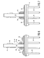
- FIG. 16 is a side view of a long header
- FIG. 17 is a top view of the header of FIG. 16 ;
- FIG. 18 is an end view of the header of FIG. 16 ;
- FIG. 19 is a bottom view of the header of FIG. 16 ;
- FIG. 20 is an enlarged detail view of the circled area labeled A of the header of FIG. 16 ;
- FIG. 21 is an enlarged detail view of the circled area labeled B of the header of FIG. 18 ;
- FIG. 22 illustrates one form of pin for use in the header of FIG. 16 ;
- FIG. 23 illustrates another form of pin for use in the header of FIG. 16 .
- PCB electrically-insulating substrate or substrate portion that has or will be provided with an electrically conductive surface or surfaces.
- substrates such as FR-4, ceramic, plastic, Teflon.
- the electrically-conductive surface is a metal pin engaging a plated through-hole in the board enabling the projecting parts of the pin to be used for connection to other components or devices.
- the pin also contacts an electrically-conductive trace or contact pad on the PCB which can be used for connection to other components or devices.
- SMT pads on the substrate surface used for the external connection or connected to a pin or solder bump contact are also known possibilities.
- a PCB such as a memory card
- edge contacts as a daughter board
- the motherboard is provided with a female connector for receiving the male pins of a plug connector, lacking on the memory card, or the memory card lacks a contact array that matches the contact array on the motherboard.
- the mounting of the daughter board to the motherboard is to be made in an in-line process which at the same time attaches further components to the motherboard.
- the daughter board is first mounted on a carrier as a connector which is chosen such that its contacts on a first surface match that of the daughter board, while the carrier's contacts on a second surface match that of the motherboard.
- in-line process is meant that, during a single reflow step, a number of interconnected boards with temporarily-mounted components and connectors can all be reflowed and thus permanently solder-bonded in the same standard process.
- the unique method of the invention first inserts into a substrate or first PCB, to serve as an edge connector, dual contacts into plated through-holes of the first PCB. These plated through-holes are surrounded by or are in contact with surface mount pads.
- FIGS. 1–7 illustrate as the first PCB an electrically-insulating carrier 10 with dual rows of plated-through holes 12 , 14 into which are inserted alternately arranged inner dual rows of short and long pins 16 , 18 .
- Both rows of inner pins form an upstanding array 20 defining a slot 22 for receiving the edge contacts of a second PCB 24 .
- Each of the pins 16 , 18 are connected to an SMT pad 26 that extends laterally on the top or first surface of the carrier 10 toward the outside edge.
- Third and fourth rows of pins 28 , 30 are also inserted in their respective plated-through holes 32 along the outer edge of the carrier. These outer pins 28 , 30 as shown extend only underneath the carrier's bottom or second surface.
- the upper parts of the pin rows 16 , 18 are previously stamped or otherwise processed to form recesses 34 on opposite sides (the sides facing away from the opposite pin) causing contact bumps or bulges or protruding regions 36 to form at the pins sides facing the edge connector receiving slot 22 as well as on the their opposite backside (which does not play a role in this embodiment).
- the latter can be omitted by configuring the recesses 34 to bulge more on the slot side than on the backside.
- FIGS. 4 and 5 show this variation with the backsides more or less flat (again of no significance in this embodiment).
- the facing bumps 36 on the inner pin sides form contact surfaces for, for example, SMT pads 38 on the edge connector of the second PCB 24 .
- Reference numerals 40 represent additional components that may be mounted on the second PCB 24 .
- each of the SMT pads 26 on the carrier 10 is deposited a controlled predetermined amount of solder 42 to serve as a solder reserve.
- the deposits 42 are physically spaced from the adjacent upstanding pin by a distance (shown at 44 in FIG. 6 ), and that region 46 of the SMT pad is coated, as for example by screen printing, with a thin layer (not shown) of a flow-resist coating, such as an Entek coating, a well-known organic resin resist material.
- a flow-resist coating such as an Entek coating, a well-known organic resin resist material.
- the flow-resist coating or surface is used on each surface mount pad 26 to limit the solder deposit from flowing down into the plated through-holes 12 , 14 and be depleted. Typically, the flow-resist coating does not burn off during a first reflow step.
- the resist coating can also obviously be selectively applied where desired by any of well-known lithographic and masking techniques.
- electrically-conductive surfaces intended for soldering are typically “tinned”, i.e., provided with a very thin solder coat of tin or similar substance that promotes wetting by the molten solder, which typically also requires fluxing to remove any thin oxides that may have formed that inhibit wetting.
- This typical “tinned” contact cannot form a reliable solder joint with a contacted counterpart “tinned” contact unless additional solder is provided that fills in and solidifies around the contact region forming the typical fillet characteristic of well-made solder joints.
- the solder deposit 42 that will provide this additional solder reserve is attached by soldering to its underlying pad and prevented from flowing away by the intervening flow-resist coating.
- This first reflow step is carried out at a temperature below that at which the flow-resist coating is burned away—or a resist is chosen that for the most part will not burn away after just one reflow step—and is just sufficient to melt the solder deposits so they will temporarily attach to the pad.
- the resultant solder bumps after the first reflow step are illustrated in FIGS. 2–6 at reference numeral 42 .
- the second PCB 24 such as the memory card, is inserted in the receiving slot 22 between the dual facing contacts 36 such that their pads 38 are in contact therewith.
- the dimensions are chosen such that the card 24 is held in place by a small interference fit in the slot 22 , shown in FIG. 6 .
- the dual contacts 36 are free of any additional solder that could obstruct insertion of the card edge.
- At least the second PCB 24 is then fluxed, or, preferably, the entire assembly is then fluxed and then run through a secondary reflow step at a higher temperature than that of the first reflow—the higher temperature may be unnecessary if a resist is chosen that will not burn away after just one reflow step but will after a second reflow step—, during which this time what remains of the flow-resist Entek coating is burned off and the molten solder from the solder deposits 42 by capillary action wicks over to the adjacent plated through-holes 12 , 14 , flows up the pins 16 , 18 , and collects on the contact junction between the pin contacts 36 and the contact surfaces of the SMT pads 38 on the memory card 24 .
- solder adheres and completely surrounds the contact sides of each of the pins and the contacted surfaces of the SMT pads on the memory card. Some solder may also go into the plated through-hole that the pin is inserted into and solders the pin into the hole, if not previously soldered.
- the solder under the influence of capillary action has formed a thicker layer 50 on the SMT pad, filled in any spaces at the plated-through-holes (not shown), and wicked up to fill any spaces at the edge contacts forming a good fillet around the joint and a robust reliable solder joint.
- the spacing 44 between the solder deposits and the adjacent plated-through or contact which is to be occupied by the flow resist coat depends on the size of the carrier or pins or pads, a larger spacing being allowed for larger carriers or pins or pads where the flow path is larger and a smaller spacing being allowed for smaller carriers or pins or pads where the flow path is smaller.
- the spacing 44 should be at a minimum about 0.001 inches, preferably about 0.003–0.06 inches. For the process where the pin is used as a transfer medium, the minimum spacing will typically be larger, about 0.02 inches.
- the size of the solder deposit similarly depends on the sizes of the carriers and pins and pads. It typically will occupy a volume of about 0.00001–0.00005 inches cubed.
- the contact region 36 on the pins is configured to have a smooth radius providing a good transitional contact point between the pin contact and the memory card edge pads and to ease insertion of the memory card between the rows of pins and before the solder is transferred and the solder joint is made.
- the excess solder would likely form irregular non-smooth regions that would interfere with the inserted card and likely prevent even contact between each of the contact regions and the corresponding edge pad on the inserted card.
- the quantity of additional solder provided is such as to also cover a plated through-hole where a pin has been inserted from the bottom side of the carrier.
- a surface mount pad at the carrier top surface or its bottom surface can be used without a bottom inserted pin.
- the contact array 20 is arranged in a specific pattern in the carrier such that a smaller PCB (daughter board or memory card) will be held perpendicular to the carrier 10 .
- PCB aughter board or memory card
- solder transfer process can be used to provide an excellent solder joint for any connection between two solderable conductive means.
- the solder can be of the conventional composition, such as 63-37 tin-lead or 90-10 tin-lead.
- the carriers 10 serving as connectors can be attached to the edge of the memory card or PCB 24 while the board is still in panel form. After fluxing the connector 10 and the SMT pads of the boards the entire panel can be reflowed. This means that the components on both sides of the boards in the panel and the added solder deposits can be reflowed at the same time. This approach eliminates the need for secondary processing or off-line manufacturing as all the components and the connectors can be reflowed in the same standard process.
- annular ring or SMT pad on the bottom surface of the carrier for each pin.
- FIG. 7 the bottom inserted pins are also shown soldered into the plated through-holes.
- the pin configuration 16 , 18 used to transfer the excess molten solder to the solder joint has straight sections, but it will be apparent that the transfer means can be of many different shapes as long as it touches the electrically-conductive surface 26 where the solder reserve 42 is deposited and also touches the electrically-conductive surface 38 of the memory card or conductive means that it is to be connected to.
- the pins 52 that serve as the solder transfer conduits between the solder deposits 42 and the contact regions 54 where the solder joints will be made are curved to provided a beveled entrance for the card.
- the bottom surface of the carrier is provided with solder balls or bumps 56 connected by means of vias (not shown) to SMT pads on the top carrier surface. The solder balls allow for easy secondary attachment using SMT processing to the motherboard instead of through-hole attachment.
- the additional solder deposit is located on a solder pad away from the electrically-conductive member having the contact region that will form part of the solder joint.
- the excess solder deposit is located on a surface region of the electrically-conductive member that is different from the surface region having the contact region that will form part of the solder joint.
- FIGS. 10–12 are examples of electrically-conductive members 60 that are punched or stamped to form a smooth preferably curved contact region 62 on a first surface and a recess or well 64 on one or more second side surfaces that are different and spaced from the contact region 62 .
- the backside surfaces 66 that do not play a role in the soldering process can be flat or curved.
- the electrically-conductive members 60 pins in this example, are inserted into a carrier 68 or other PCB before the wells 64 are filled with solder to serve as the additional solder reserve.
- a typical carrier 68 with its SMT pads 70 connected to the inserted pins is illustrated in FIG. 13 .
- a solder mask is provided (not shown) everywhere except inside the well surfaces, and then the well side of the board is run through a wave solder process which causes molten solder to fill the wells 64 on the sides, and upon cooling solidifies to form the desired solid mass of excess solder, shown at 72 in FIG. 14 , as well as to solder the pins into the plated through-holes.
- reserve solder 72 fills both wells 64 on the side surfaces of the pin.
- the additional solder 72 is spaced from the contact surfaces 62 which remain free of any obstructions that may interfere with insertion of the second PCB or prevent proper contact between all of the contact regions 62 and the corresponding contact regions of the second PCB.
- the flow-resistant coating that prevented improper spread of the solder during the wave solder step is then removed by any convenient means, or as before the second reflow is used to burn off the flow-resistant coating.
- the assembly is subjected to a second reflow (counting the wave solder step as a first reflow) during which process the molten solder from the solder deposits 72 by capillary action wick around the pins and collect on the contact junction between the pin contacts regions 62 and the contact surfaces of the SMT pads 74 on the inserted card 76 , and can flow as well into the plated through-holes.
- the solder adheres and completely surrounds the contact sides of each of the pins and the contacted surfaces of the SMT pads on the memory card. Some solder also goes into the plated through-hole that the pin is inserted into and solders the pin into the hole.
- the solder under the influence of capillary action has formed a thicker layer 80 on the SMT pad, filled in any spaces in the plated-through holes (not shown), and wicked around to fill any spaces at the edge contact array 74 forming a good fillet around the joint and a robust reliable solder joint.
- the contact member used in the invention can be fabricated with different cross-sections, such as round, square, rectangular, and octagonal, etc. It can also have different shapes, and be fabricated by techniques in addition to stamping and punching, such as by using a screw machine approach or cold heading to make the pin rather than by stamping.
- the invention can be used with any kind of substrate that has openings into which a projecting member needs to be mounted by placement in the holes or can use solder bumps or other forms of interconnections.
- the invention can also be applied to projecting members from sockets or clips that will be soldered to an inserted component to be mounted onto a substrate.
- FIG. 15 illustrates a modified pin design of the screw machine type, comprising an electrically-conductive member 84 having a post 86 for mounting to a substrate, and a contact part 88 .
- the latter has a curved top with a widened part designated 88 that forms the contact region that makes contact with the pads on the card when inserted between two lines of posts of the type illustrated.
- the contact region 88 Spaced below and above, respectively, the contact region 88 are annular recesses 90 , 92 which receive the solder deposits (not shown).
- the latter can be achieved by masking all but the recesses and wave soldering or other equivalent means that results in solidified melted solder filling the recesses 90 , 92 .
- the solidified solder (not shown in FIG.
- solderable material such as copper or copper alloy, brass or brass alloy, and phosphor bronze
- the overall pin lengths can cover a wide range, for example, from 0.25–2 inches.
- solder reserve before transfer, preferably is a mass of solid material, which is preferably melted solder, preferably formed by a separate reflow step, and is not wet solder paste or any other kind of non-solid material.
- FIGS. 16–23 illustrate another embodiment of the invention in a somewhat different context than the previous embodiments.
- a problem arises when attempting to surface mount a relatively long header with multiple pins to solder pads on a PCB.
- header is meant an insulating member, typically in the form of a small plate-like member, supporting a plurality of spaced pins.
- the pins are typically arrayed in one or more parallel rows.
- the pin arrangement can function to receive a female connector whose socket openings match the array of pins, or itself can be used as contacts to another PCB.
- An entire header is intended to be soldered to similarly arrayed solder pads on the PCB, meaning that each pin foot, which protrudes below the header, is surface mounted by solder to one of the pads.
- the header length is longer than about one inch, especially with pins that have an extended mounting contact surface area, it is possible that the pin footprints are not exactly coplanar or not exactly parallel to the plane of the contact pads. As a result, gaps may arise between some of the solder footprints and their underlying pads, which could detrimentally affect the robustness of the solder bond of that or those pin(s) to the underlying pad.
- An attempt to resolve this problem has been made by adding a layer of solder paste to each of the pads before placing the header pins in contact with the pads. But this has not completely solved the problem, in that the solder paste does not provide enough additional solder during the remelt process to ensure robust connections between each of the pins and their contacted pads.
- a solder reserve of hardened preflowed solder is provided in a well on the foot of each pin on at least one of the pin sides, preferably both pin sides.
- the reserve is not on the footprint of the pin, as this could aggravate the problem of uniform robust solder joints.
- solder from the reserve remelts and flows down the pin sides to the contact region of the pin footprint and pad. This reserve provides enough additional solder at the joint to ensure that all the pins of the header are robustly solder connected to their respective pad even if not fully contacted to the pad or being slightly awry.
- pin foot is meant the portion of the pin below the header, and by “pin or contact portion” is meant the portion of the pin extending above the header. It is understood that the terms “above” and “below” are used for illustrative purposes and explanatory purposes, as such objects are frequently illustrated with the foot below the header, but it is not meant to be restricting since, obviously, after the solder operation, the PCB may be positioned sideways or upside down in which case the header foot could be positioned laterally or above the header, and such orientations are to be deemed also within the scope of the invention.
- footprint is meant the surface area of the bottom surface of the foot intended to be placed in contact with the PCB pad, and by “extended surface mounting area” is meant a pin footprint whose contact surface area is at least about twice the cross-sectional area of just the pin portion itself.
- a good example of such a pin which is not meant to be limiting, is the so-called SPACESAVER surface mount pin headers sold by Autosplice Inc., of San Diego, Calif.
- a typical header has a typically square pin of 0.025 inches per side (surface area of 0.000625 square inches), with a footprint contact area at the pin foot bottom of 0.025 by 0.060 inches (surface area of 0.0015 square inches), or about 2.4 times larger than the pin cross-section.
- This configuration produces what can be called a flattened foot with two opposed broad sides and two opposed narrow sides.
- the lack of pin footprint coplanarity is worse for the long header situation, which ideally requires, say, 12 or more pins arrayed in two rows to be in full surface contact with 12 pads.
- the problem becomes much worse for a so-called PR-4 header containing on one side 40 pins arrayed in two parallel rows, and on the other side 32 pins arrayed in two additional parallel rows, designed for receiving a 40 pin and/or a 32 pin female connector.
- a well is provided at a side surface of the pin foot but spaced just above the pin footprint.
- the well is at the broad surface of the pin foot, and preferably a well is provided at opposite broad surfaces.
- well is meant an open blind recess which is thus exposed at its opening and thus any material stored in the well is also exposed at the side of the foot and thus can readily flow out when remelted.
- reflowed solidified solder is melted into the well or wells and thus acts as a solder reserve when the pin is surface mounted to its pad on the PCB.
- FIGS. 16–19 illustrates a typical SPACESAVER header 98 whose electrically-insulating pin support is referenced 100 , and the pins 102 , 103 .
- the PCB can be similar to that illustrated in FIG. 14 with its solder pads on the board designated 70 , except that the upstanding posts typically are not present
- a PCB 120 is shown in dashed lines. Its pads are shown at 122 , each underlying one pin foot What is not shown is a layer of solder paste that is typically provided on the pads before the header is amounted.
- the paste layer thickness is not critical and can be about 0.003–0.006 inches thick.
- the two pins 102 , 103 are shown in enlarged view in perspective in FIGS. 22 and 23 .
- Each of the pins comprises a foot 106 , and a pin portion 108 , with the former below the header support 100 and the latter above as shown in FIG. 16 .
- Each of the broad sides 110 of the pin foot is provided with a small cavity or well designated 112 , each of which wells on each of the pins is filled with solid preflowed solder 114 before the header 98 is placed on the board.
- FIGS. 22 and 23 for simplicity show the wells empty, but the solder reserve deposit 114 is shown in FIGS. 20 and 21 .
- the solder reserve deposit 114 typically fills most or all of the well 112 .
- the wells are pre-filled with solder by selectively applying a solder wettable material in each well, or a solder non-wettable material everywhere but in the wells (e.g., by selectively plating in the appropriate way), and then passing the header through a wave solder process where the molten solder selectively sticks to the well interior and hardens during cooling
- the header e.g., by selectively plating in the appropriate way
- the entire foot 106 from the well top downward, then, is tin-plated that is, coated with a high-solder flow promoting surface, whereas the pin portion 108 above is coated with a low-solder-flow material such as nickel.
- the melted-solder from the reserve tends to flow or wick along the high-flow surface toward the pin footprints, which is the bottom contact surface designated 116 .
- the low-solder-flow material coating can terminate about halfway up the pin portion 108 , and the remainder gold coated to ensure a good connection with the connector sockets.
- the well bottom terminates just above the pin footprint 116 .
- the spacing of the well bottom and thus of the lowest point of the reserve deposit from the footprint is at least about 0.002 inches, preferably at least about 0.004 inches.
- the spacing should slightly less than the solder paste thickness to ensure that the solder paste slightly overlaps and contacts the well solder deposit, which promotes solder flow to the footprint.
- the well 112 in the smaller pin was about 0.028 ⁇ 0.050 ⁇ 0.009 inches deep. Preferably the well depth exceeds about 0.005 inches.
- the pin portion was 0.025 inches square and the footprint was about 0.025 ⁇ 0.060 inches. These drawings are approximately to scale.
- the pin header illustrated was of the PR-4 type previously mentioned.
- the well volume and the reserve volume should be sufficient such that adequate additional solder from the reserve is provided at the joint during the second reflow. From the examples given, it was found that adequate additional solder can be made available from the reserve to ensure robust solder joints even when there was as much as a 0.005–0.010 inches gap between, a pin footprint and a pad surface.
- the pins 102 , 103 are preferably pre-soldered into their respective holes in the header 100 by means of a higher-temperate solder than that used for the reserve deposit.
- the higher-temperature solder acts as a plug or barrier in the header through-holes to upward solder flow during the second reflow, which is carried out at a lower-temperature sufficient to melt the reserve deposit but not the high-temperature plug.
- the solder in each of the reserves wicks down the pin sides and will supply the additional solder needed to fill any possible contact gaps between the pin bottoms and the pads.
- the pins are conventionally tinned, but this tinning does not provide sufficient additional solder to solve the problems described above.
Abstract
Description
Claims (25)
Priority Applications (1)
| Application Number | Priority Date | Filing Date | Title |
|---|---|---|---|
| US10/843,972 US6976855B2 (en) | 2002-12-06 | 2004-05-13 | Solder reserve transfer device and process |
Applications Claiming Priority (2)
| Application Number | Priority Date | Filing Date | Title |
|---|---|---|---|
| US10/310,215 US6780028B1 (en) | 2002-12-06 | 2002-12-06 | Solder reserve transfer device and process |
| US10/843,972 US6976855B2 (en) | 2002-12-06 | 2004-05-13 | Solder reserve transfer device and process |
Related Parent Applications (1)
| Application Number | Title | Priority Date | Filing Date |
|---|---|---|---|
| US10/310,215 Continuation-In-Part US6780028B1 (en) | 2002-12-06 | 2002-12-06 | Solder reserve transfer device and process |
Publications (2)
| Publication Number | Publication Date |
|---|---|
| US20040209495A1 US20040209495A1 (en) | 2004-10-21 |
| US6976855B2 true US6976855B2 (en) | 2005-12-20 |
Family
ID=32312265
Family Applications (2)
| Application Number | Title | Priority Date | Filing Date |
|---|---|---|---|
| US10/310,215 Expired - Fee Related US6780028B1 (en) | 2002-12-06 | 2002-12-06 | Solder reserve transfer device and process |
| US10/843,972 Expired - Fee Related US6976855B2 (en) | 2002-12-06 | 2004-05-13 | Solder reserve transfer device and process |
Family Applications Before (1)
| Application Number | Title | Priority Date | Filing Date |
|---|---|---|---|
| US10/310,215 Expired - Fee Related US6780028B1 (en) | 2002-12-06 | 2002-12-06 | Solder reserve transfer device and process |
Country Status (4)
| Country | Link |
|---|---|
| US (2) | US6780028B1 (en) |
| EP (1) | EP1427073A1 (en) |
| JP (1) | JP2004207232A (en) |
| KR (1) | KR20040049813A (en) |
Cited By (8)
| Publication number | Priority date | Publication date | Assignee | Title |
|---|---|---|---|---|
| US20060040517A1 (en) * | 2004-08-19 | 2006-02-23 | Sumitomo Wiring Systems, Ltd. | Method of mounting terminal on printed board, terminal mounted printed board and electric connection box accommodating the terminal mounted printed board, which are formed by the method |
| US20060264107A1 (en) * | 2005-05-20 | 2006-11-23 | Tsai Chou H | Electrical connector assembled with a bondable element |
| US20080009155A1 (en) * | 2005-06-07 | 2008-01-10 | Shinko Electric Industries Co., Ltd. | Wiring board with lead pins, and lead pin |
| US20090038823A1 (en) * | 2007-08-07 | 2009-02-12 | Shinko Electric Industries Co., Ltd. | Wiring substrate with lead pin and lead pin |
| US20110217853A1 (en) * | 2009-09-11 | 2011-09-08 | Thales | Connection Device for High Frequency Signals Between a Connector and a Transmission Line |
| US20120202371A1 (en) * | 2009-10-06 | 2012-08-09 | Phonak Ag | Integral connector for programming a hearing device |
| US9577350B2 (en) * | 2014-01-23 | 2017-02-21 | Delta Electronics (Shanghai) Co., Ltd. | Pin and a printed circuit board |
| US20180247768A1 (en) * | 2015-02-27 | 2018-08-30 | Epcos Ag | Electrical component and a method for producing an electrical component |
Families Citing this family (19)
| Publication number | Priority date | Publication date | Assignee | Title |
|---|---|---|---|---|
| US6760028B1 (en) * | 2000-07-21 | 2004-07-06 | Microsoft Corporation | Methods and systems for hinting fonts |
| KR20040061250A (en) * | 2002-12-30 | 2004-07-07 | 삼성전자주식회사 | Printed circuit board which can be connected with pin connector and manufacturing method the same |
| JP4537732B2 (en) * | 2004-03-04 | 2010-09-08 | 住友電装株式会社 | Board connector |
| FR2872072B1 (en) * | 2004-06-24 | 2006-09-29 | Snecma Propulsion Solide Sa | METHOD OF BRAZING PARTS OF SILICURE THERMOSTRUCTURAL COMPOSITE MATERIAL |
| JP2006244731A (en) * | 2005-02-28 | 2006-09-14 | Molex Inc | Terminal and connector using this terminal |
| US7156678B2 (en) * | 2005-04-07 | 2007-01-02 | 3M Innovative Properties Company | Printed circuit connector assembly |
| US7338292B2 (en) * | 2006-01-26 | 2008-03-04 | Agilent Technologies, Inc. | Board-to-board electronic interface using hemi-ellipsoidal surface features |
| TW200812445A (en) * | 2006-08-18 | 2008-03-01 | Wintek Corp | Connection structure of printed-circuit board in LCD module |
| JP4828361B2 (en) * | 2006-09-15 | 2011-11-30 | 株式会社フジクラ | Method for preventing solder from rising onto electrical contact and electrical contact using the method |
| FR2906644B1 (en) * | 2006-09-29 | 2008-12-26 | Intexys Sa Sa | METHOD AND DEVICE FOR CONNECTING ELECTRONIC AND / OR OPTOELECTRONIC CIRCUITS. |
| DE102007058095A1 (en) * | 2007-12-03 | 2009-06-04 | Robert Bosch Gmbh | Printed circuit board with contact pins connected to it |
| DE102009055859A1 (en) * | 2009-11-26 | 2011-06-01 | Osram Gesellschaft mit beschränkter Haftung | Method for contacting a both sides provided with electrical contacts printed circuit board and such circuit board |
| US9136624B1 (en) * | 2013-03-28 | 2015-09-15 | Juniper Networks, Inc. | Orthogonal cross-connecting of printed circuit boards without a midplane board |
| FR3007216B1 (en) | 2013-06-12 | 2017-01-13 | Valeo Vision | ELECTRICAL CONNECTION CLAMP FOR PLATINUM WITH LIGHTING LED |
| CN110783727A (en) * | 2018-11-09 | 2020-02-11 | 广州方邦电子股份有限公司 | Connector and manufacturing method |
| US11033990B2 (en) * | 2018-11-29 | 2021-06-15 | Raytheon Company | Low cost approach for depositing solder and adhesives in a pattern for forming electronic assemblies |
| CN109604754B (en) * | 2018-12-12 | 2021-10-22 | 惠州光弘科技股份有限公司 | Reflow soldering method for improving thermal expansion deformation of device |
| DE102019128179A1 (en) * | 2019-10-18 | 2021-04-22 | Webasto SE | Electrical connection system for connecting a circuit board to a connector via an electrical connection device |
| EP4133574A1 (en) * | 2020-04-07 | 2023-02-15 | Milwaukee Electric Tool Corporation | Impact tool and electric motor |
Citations (25)
| Publication number | Priority date | Publication date | Assignee | Title |
|---|---|---|---|---|
| US3601750A (en) * | 1970-02-09 | 1971-08-24 | Berg Electronics Inc | Circuit board connector |
| US4500149A (en) * | 1982-07-28 | 1985-02-19 | At&T Technologies, Inc. | Solder-bearing lead |
| US4646204A (en) * | 1986-02-10 | 1987-02-24 | Rca Corporation | Hole geometry for printed circuit boards |
| US4655517A (en) * | 1985-02-15 | 1987-04-07 | Crane Electronics, Inc. | Electrical connector |
| US4663815A (en) * | 1985-06-21 | 1987-05-12 | Associated Enterprises, Inc. | A method and apparatus for surface mount compatible connector system with mechanical integrity |
| US4797110A (en) * | 1986-09-08 | 1989-01-10 | General Motors Corporation | Printed circuit board with integral electrical connector and method for making it using wave soldering |
| US4855517A (en) * | 1984-08-30 | 1989-08-08 | Hoechst Aktiengesellschaft | Process for preparing aromatic bromine compounds |
| US4854472A (en) * | 1988-06-10 | 1989-08-08 | Plastic Technologies, Inc. | Tamper resistant wide mouth package with dynamic seal |
| US4877176A (en) * | 1987-11-25 | 1989-10-31 | Northern Telecom Limited | Soldering pins into printed circuit boards |
| US4884335A (en) * | 1985-06-21 | 1989-12-05 | Minnesota Mining And Manufacturing Company | Surface mount compatible connector system with solder strip and mounting connector to PCB |
| US4943846A (en) * | 1989-11-09 | 1990-07-24 | Amp Incorporated | Pin grid array having seperate posts and socket contacts |
| US5033675A (en) * | 1986-10-13 | 1991-07-23 | Sharp Kabushiki Kaisha | Connector |
| US5035656A (en) * | 1990-05-15 | 1991-07-30 | E. I. Du Pont De Nemours And Company | Connector, circuit board contact element and retention portion |
| US5169347A (en) * | 1991-10-15 | 1992-12-08 | Molex Incorporated | Slip-off electrical connector header |
| US5641291A (en) * | 1993-12-13 | 1997-06-24 | Japan Solderless Terminal Mfg. Co., Ltd. | Printed circuit board connector |
| US5656798A (en) * | 1992-09-21 | 1997-08-12 | Matsushita Electric Works, Ltd. | Terminal-carrying circuit board |
| US5816868A (en) * | 1996-02-12 | 1998-10-06 | Zierick Manufacturing Corp. | Capillary action promoting surface mount connectors |
| US6011222A (en) * | 1995-12-15 | 2000-01-04 | Ibiden Co., Ltd. | Substrate for mounting electronic part |
| US6116921A (en) * | 1998-02-16 | 2000-09-12 | The Whitaker Corporation | Electrical connector having recessed solderball foot |
| US6259039B1 (en) * | 1998-12-29 | 2001-07-10 | Intel Corporation | Surface mount connector with pins in vias |
| US6402574B2 (en) * | 1995-11-03 | 2002-06-11 | North American Specialties Corporation | Solder-holding clips for applying solder to connectors or the like |
| US6402531B1 (en) * | 1998-10-05 | 2002-06-11 | Zierick Manufacturing Corp. | Capillary action enhanced surface mount pin header |
| US6623283B1 (en) * | 2000-03-08 | 2003-09-23 | Autosplice, Inc. | Connector with base having channels to facilitate surface mount solder attachment |
| US6644983B2 (en) * | 2001-02-09 | 2003-11-11 | International Business Machines Corporation | Contact assembly, connector assembly utilizing same, and electronic assembly |
| US6773269B1 (en) * | 2002-09-27 | 2004-08-10 | Emc Corporation | Circuit board assembly which utilizes a pin assembly and techniques for making the same |
Family Cites Families (4)
| Publication number | Priority date | Publication date | Assignee | Title |
|---|---|---|---|---|
| US5139448A (en) * | 1985-05-24 | 1992-08-18 | North American Specialties Corporation | Solder-bearing lead |
| US4767344A (en) * | 1986-08-22 | 1988-08-30 | Burndy Corporation | Solder mounting of electrical contacts |
| JP3667786B2 (en) * | 1994-03-17 | 2005-07-06 | インテル・コーポレーション | IC socket and inspection method of conductive connection state with printed circuit board |
| US5490788A (en) * | 1994-11-01 | 1996-02-13 | Emc Technology, Inc. | Surface mount terminal for electrical component |
-
2002
- 2002-12-06 US US10/310,215 patent/US6780028B1/en not_active Expired - Fee Related
-
2003
- 2003-12-01 EP EP03027454A patent/EP1427073A1/en not_active Withdrawn
- 2003-12-05 KR KR1020030087915A patent/KR20040049813A/en not_active Application Discontinuation
- 2003-12-08 JP JP2003409693A patent/JP2004207232A/en active Pending
-
2004
- 2004-05-13 US US10/843,972 patent/US6976855B2/en not_active Expired - Fee Related
Patent Citations (26)
| Publication number | Priority date | Publication date | Assignee | Title |
|---|---|---|---|---|
| US3601750A (en) * | 1970-02-09 | 1971-08-24 | Berg Electronics Inc | Circuit board connector |
| US4500149A (en) * | 1982-07-28 | 1985-02-19 | At&T Technologies, Inc. | Solder-bearing lead |
| US4855517A (en) * | 1984-08-30 | 1989-08-08 | Hoechst Aktiengesellschaft | Process for preparing aromatic bromine compounds |
| US4655517A (en) * | 1985-02-15 | 1987-04-07 | Crane Electronics, Inc. | Electrical connector |
| US4663815A (en) * | 1985-06-21 | 1987-05-12 | Associated Enterprises, Inc. | A method and apparatus for surface mount compatible connector system with mechanical integrity |
| US4884335A (en) * | 1985-06-21 | 1989-12-05 | Minnesota Mining And Manufacturing Company | Surface mount compatible connector system with solder strip and mounting connector to PCB |
| US4646204A (en) * | 1986-02-10 | 1987-02-24 | Rca Corporation | Hole geometry for printed circuit boards |
| US4797110A (en) * | 1986-09-08 | 1989-01-10 | General Motors Corporation | Printed circuit board with integral electrical connector and method for making it using wave soldering |
| US5033675A (en) * | 1986-10-13 | 1991-07-23 | Sharp Kabushiki Kaisha | Connector |
| US4877176A (en) * | 1987-11-25 | 1989-10-31 | Northern Telecom Limited | Soldering pins into printed circuit boards |
| US4854472A (en) * | 1988-06-10 | 1989-08-08 | Plastic Technologies, Inc. | Tamper resistant wide mouth package with dynamic seal |
| US4943846A (en) * | 1989-11-09 | 1990-07-24 | Amp Incorporated | Pin grid array having seperate posts and socket contacts |
| US5035656A (en) * | 1990-05-15 | 1991-07-30 | E. I. Du Pont De Nemours And Company | Connector, circuit board contact element and retention portion |
| US5169347A (en) * | 1991-10-15 | 1992-12-08 | Molex Incorporated | Slip-off electrical connector header |
| US5656798A (en) * | 1992-09-21 | 1997-08-12 | Matsushita Electric Works, Ltd. | Terminal-carrying circuit board |
| US5641291A (en) * | 1993-12-13 | 1997-06-24 | Japan Solderless Terminal Mfg. Co., Ltd. | Printed circuit board connector |
| US6402574B2 (en) * | 1995-11-03 | 2002-06-11 | North American Specialties Corporation | Solder-holding clips for applying solder to connectors or the like |
| US6229101B1 (en) * | 1995-12-15 | 2001-05-08 | Ibiden Co. Ltd. | Substrate for mounting electronic part |
| US6011222A (en) * | 1995-12-15 | 2000-01-04 | Ibiden Co., Ltd. | Substrate for mounting electronic part |
| US5816868A (en) * | 1996-02-12 | 1998-10-06 | Zierick Manufacturing Corp. | Capillary action promoting surface mount connectors |
| US6116921A (en) * | 1998-02-16 | 2000-09-12 | The Whitaker Corporation | Electrical connector having recessed solderball foot |
| US6402531B1 (en) * | 1998-10-05 | 2002-06-11 | Zierick Manufacturing Corp. | Capillary action enhanced surface mount pin header |
| US6259039B1 (en) * | 1998-12-29 | 2001-07-10 | Intel Corporation | Surface mount connector with pins in vias |
| US6623283B1 (en) * | 2000-03-08 | 2003-09-23 | Autosplice, Inc. | Connector with base having channels to facilitate surface mount solder attachment |
| US6644983B2 (en) * | 2001-02-09 | 2003-11-11 | International Business Machines Corporation | Contact assembly, connector assembly utilizing same, and electronic assembly |
| US6773269B1 (en) * | 2002-09-27 | 2004-08-10 | Emc Corporation | Circuit board assembly which utilizes a pin assembly and techniques for making the same |
Cited By (15)
| Publication number | Priority date | Publication date | Assignee | Title |
|---|---|---|---|---|
| US20060040517A1 (en) * | 2004-08-19 | 2006-02-23 | Sumitomo Wiring Systems, Ltd. | Method of mounting terminal on printed board, terminal mounted printed board and electric connection box accommodating the terminal mounted printed board, which are formed by the method |
| US7311241B2 (en) * | 2004-08-19 | 2007-12-25 | Sumitomo Wiring Systems, Ltd. | Method of mounting terminal on printed board, terminal mounted printed board and electric connection box accommodating the terminal mounted printed board, which are formed by the method |
| US20060264107A1 (en) * | 2005-05-20 | 2006-11-23 | Tsai Chou H | Electrical connector assembled with a bondable element |
| US7476109B2 (en) * | 2005-05-20 | 2009-01-13 | Chou Hsuan Tsai | Electrical connector assembled with a bondable element |
| US20080009155A1 (en) * | 2005-06-07 | 2008-01-10 | Shinko Electric Industries Co., Ltd. | Wiring board with lead pins, and lead pin |
| US7422449B2 (en) * | 2005-06-07 | 2008-09-09 | Shinko Electric Industries Co., Ltd. | Wiring board with lead pins, and lead pin |
| US20090038823A1 (en) * | 2007-08-07 | 2009-02-12 | Shinko Electric Industries Co., Ltd. | Wiring substrate with lead pin and lead pin |
| US20110217853A1 (en) * | 2009-09-11 | 2011-09-08 | Thales | Connection Device for High Frequency Signals Between a Connector and a Transmission Line |
| US8540523B2 (en) * | 2009-09-11 | 2013-09-24 | Thales | Connection device for high frequency signals between a connector and a transmission line |
| US20120202371A1 (en) * | 2009-10-06 | 2012-08-09 | Phonak Ag | Integral connector for programming a hearing device |
| US8651895B2 (en) * | 2009-10-06 | 2014-02-18 | Phonak Ag | Integral connector for programming a hearing device |
| US9577350B2 (en) * | 2014-01-23 | 2017-02-21 | Delta Electronics (Shanghai) Co., Ltd. | Pin and a printed circuit board |
| US20180247768A1 (en) * | 2015-02-27 | 2018-08-30 | Epcos Ag | Electrical component and a method for producing an electrical component |
| US10943740B2 (en) | 2015-02-27 | 2021-03-09 | Epcos Ag | Electrical connection contact for a ceramic component, a ceramic component, and a component arrangement |
| US11342126B2 (en) * | 2015-02-27 | 2022-05-24 | Epcos Ag | Electrical component and a method for producing an electrical component |
Also Published As
| Publication number | Publication date |
|---|---|
| JP2004207232A (en) | 2004-07-22 |
| US6780028B1 (en) | 2004-08-24 |
| KR20040049813A (en) | 2004-06-12 |
| US20040209495A1 (en) | 2004-10-21 |
| EP1427073A1 (en) | 2004-06-09 |
Similar Documents
| Publication | Publication Date | Title |
|---|---|---|
| US6976855B2 (en) | Solder reserve transfer device and process | |
| US6259039B1 (en) | Surface mount connector with pins in vias | |
| EP0480754B1 (en) | Mounting device for mounting an electronic device on a substrate by the surface mounting technology | |
| US7168964B2 (en) | High density connector and method of manufacture | |
| US6164983A (en) | High density connector | |
| US6300578B1 (en) | Pad-on-via assembly technique | |
| US6623283B1 (en) | Connector with base having channels to facilitate surface mount solder attachment | |
| US6454157B2 (en) | High density connector having a ball type of contact surface | |
| US5463191A (en) | Circuit board having an improved fine pitch ball grid array and method of assembly therefor | |
| JP2018174018A (en) | socket | |
| US7484971B2 (en) | Electronic component with high density, low cost attachment | |
| GB2242579A (en) | Electrical connectors for flat insulated boards | |
| US6333471B1 (en) | Sheet metal component for double pattern conduction and printed circuit board | |
| JP2003217720A (en) | Pin grid array electrical connector | |
| GB2435350A (en) | Interconnection device for a double sided PCB | |
| EP1311031B1 (en) | High density connector | |
| EP0670760B1 (en) | Electrical connector | |
| JP4112118B2 (en) | Contact manufacturing method and connector | |
| JPH07170061A (en) | Mounting of electric component | |
| JPH11219741A (en) | Solder ball contact and solder ball connector | |
| CA2455080C (en) | High density connector and method of manufacture | |
| EP1536522B1 (en) | High density connector having a ball type of contact surface | |
| TW554580B (en) | Electric connector with coating of anti-soldering ink and its manufacturing method | |
| JP2001298264A (en) | Solder chip | |
| JPH0738219A (en) | Double-sided printed circuit board |
Legal Events
| Date | Code | Title | Description |
|---|---|---|---|
| AS | Assignment |
Owner name: AUTOSPLICE SYSTEMS INC., CALIFORNIA Free format text: ASSIGNMENT OF ASSIGNORS INTEREST;ASSIGNORS:KENNEDY, CRAIG M.;EISENBERG, DONALD S.;REEL/FRAME:015329/0959 Effective date: 20040506 |
|
| REMI | Maintenance fee reminder mailed | ||
| FPAY | Fee payment |
Year of fee payment: 4 |
|
| SULP | Surcharge for late payment | ||
| FEPP | Fee payment procedure |
Free format text: PAT HOLDER NO LONGER CLAIMS SMALL ENTITY STATUS, ENTITY STATUS SET TO UNDISCOUNTED (ORIGINAL EVENT CODE: STOL); ENTITY STATUS OF PATENT OWNER: LARGE ENTITY |
|
| SULP | Surcharge for late payment | ||
| REMI | Maintenance fee reminder mailed | ||
| FEPP | Fee payment procedure |
Free format text: PETITION RELATED TO MAINTENANCE FEES GRANTED (ORIGINAL EVENT CODE: PMFG); ENTITY STATUS OF PATENT OWNER: LARGE ENTITY Free format text: PETITION RELATED TO MAINTENANCE FEES FILED (ORIGINAL EVENT CODE: PMFP); ENTITY STATUS OF PATENT OWNER: LARGE ENTITY |
|
| LAPS | Lapse for failure to pay maintenance fees | ||
| REIN | Reinstatement after maintenance fee payment confirmed | ||
| PRDP | Patent reinstated due to the acceptance of a late maintenance fee |
Effective date: 20140130 |
|
| FPAY | Fee payment |
Year of fee payment: 8 |
|
| SULP | Surcharge for late payment | ||
| FP | Lapsed due to failure to pay maintenance fee |
Effective date: 20131220 |
|
| AS | Assignment |
Owner name: MEDLEY CAPITAL CORPORATION, AS AGENT, NEW YORK Free format text: SECURITY INTEREST;ASSIGNOR:AUTOSPLICE, INC.;REEL/FRAME:033263/0447 Effective date: 20140630 |
|
| AS | Assignment |
Owner name: WELLS FARGO BANK NATIONAL ASSOCIATION, CALIFORNIA Free format text: SECURITY INTEREST;ASSIGNOR:AUTOSPLICE, INC.;REEL/FRAME:034587/0542 Effective date: 20140917 |
|
| REMI | Maintenance fee reminder mailed | ||
| LAPS | Lapse for failure to pay maintenance fees |
Free format text: PATENT EXPIRED FOR FAILURE TO PAY MAINTENANCE FEES (ORIGINAL EVENT CODE: EXP.) |
|
| STCH | Information on status: patent discontinuation |
Free format text: PATENT EXPIRED DUE TO NONPAYMENT OF MAINTENANCE FEES UNDER 37 CFR 1.362 |
|
| FP | Lapsed due to failure to pay maintenance fee |
Effective date: 20171220 |
|
| AS | Assignment |
Owner name: AUTOSPLICE, INC., CALIFORNIA Free format text: RELEASE AND TERMINATION OF SECURITY INTERESTS IN PATENTS;ASSIGNOR:MEDLEY CAPITAL CORPORATION, AS AGENT;REEL/FRAME:058957/0300 Effective date: 20211122 |