US5169347A - Slip-off electrical connector header - Google Patents
Slip-off electrical connector header Download PDFInfo
- Publication number
- US5169347A US5169347A US07/777,830 US77783091A US5169347A US 5169347 A US5169347 A US 5169347A US 77783091 A US77783091 A US 77783091A US 5169347 A US5169347 A US 5169347A
- Authority
- US
- United States
- Prior art keywords
- block
- pins
- pin
- passages
- insulator block
- Prior art date
- Legal status (The legal status is an assumption and is not a legal conclusion. Google has not performed a legal analysis and makes no representation as to the accuracy of the status listed.)
- Expired - Fee Related
Links
Images

Classifications
-
- H—ELECTRICITY
- H01—ELECTRIC ELEMENTS
- H01R—ELECTRICALLY-CONDUCTIVE CONNECTIONS; STRUCTURAL ASSOCIATIONS OF A PLURALITY OF MUTUALLY-INSULATED ELECTRICAL CONNECTING ELEMENTS; COUPLING DEVICES; CURRENT COLLECTORS
- H01R12/00—Structural associations of a plurality of mutually-insulated electrical connecting elements, specially adapted for printed circuits, e.g. printed circuit boards [PCB], flat or ribbon cables, or like generally planar structures, e.g. terminal strips, terminal blocks; Coupling devices specially adapted for printed circuits, flat or ribbon cables, or like generally planar structures; Terminals specially adapted for contact with, or insertion into, printed circuits, flat or ribbon cables, or like generally planar structures
- H01R12/70—Coupling devices
- H01R12/71—Coupling devices for rigid printing circuits or like structures
- H01R12/72—Coupling devices for rigid printing circuits or like structures coupling with the edge of the rigid printed circuits or like structures
-
- H—ELECTRICITY
- H01—ELECTRIC ELEMENTS
- H01R—ELECTRICALLY-CONDUCTIVE CONNECTIONS; STRUCTURAL ASSOCIATIONS OF A PLURALITY OF MUTUALLY-INSULATED ELECTRICAL CONNECTING ELEMENTS; COUPLING DEVICES; CURRENT COLLECTORS
- H01R43/00—Apparatus or processes specially adapted for manufacturing, assembling, maintaining, or repairing of line connectors or current collectors or for joining electric conductors
- H01R43/20—Apparatus or processes specially adapted for manufacturing, assembling, maintaining, or repairing of line connectors or current collectors or for joining electric conductors for assembling or disassembling contact members with insulating base, case or sleeve
- H01R43/205—Apparatus or processes specially adapted for manufacturing, assembling, maintaining, or repairing of line connectors or current collectors or for joining electric conductors for assembling or disassembling contact members with insulating base, case or sleeve with a panel or printed circuit board
-
- H—ELECTRICITY
- H01—ELECTRIC ELEMENTS
- H01R—ELECTRICALLY-CONDUCTIVE CONNECTIONS; STRUCTURAL ASSOCIATIONS OF A PLURALITY OF MUTUALLY-INSULATED ELECTRICAL CONNECTING ELEMENTS; COUPLING DEVICES; CURRENT COLLECTORS
- H01R13/00—Details of coupling devices of the kinds covered by groups H01R12/70 or H01R24/00 - H01R33/00
- H01R13/02—Contact members
- H01R13/04—Pins or blades for co-operation with sockets
-
- H—ELECTRICITY
- H01—ELECTRIC ELEMENTS
- H01R—ELECTRICALLY-CONDUCTIVE CONNECTIONS; STRUCTURAL ASSOCIATIONS OF A PLURALITY OF MUTUALLY-INSULATED ELECTRICAL CONNECTING ELEMENTS; COUPLING DEVICES; CURRENT COLLECTORS
- H01R12/00—Structural associations of a plurality of mutually-insulated electrical connecting elements, specially adapted for printed circuits, e.g. printed circuit boards [PCB], flat or ribbon cables, or like generally planar structures, e.g. terminal strips, terminal blocks; Coupling devices specially adapted for printed circuits, flat or ribbon cables, or like generally planar structures; Terminals specially adapted for contact with, or insertion into, printed circuits, flat or ribbon cables, or like generally planar structures
- H01R12/70—Coupling devices
- H01R12/71—Coupling devices for rigid printing circuits or like structures
- H01R12/712—Coupling devices for rigid printing circuits or like structures co-operating with the surface of the printed circuit or with a coupling device exclusively provided on the surface of the printed circuit
- H01R12/716—Coupling device provided on the PCB
- H01R12/718—Contact members provided on the PCB without an insulating housing
-
- Y—GENERAL TAGGING OF NEW TECHNOLOGICAL DEVELOPMENTS; GENERAL TAGGING OF CROSS-SECTIONAL TECHNOLOGIES SPANNING OVER SEVERAL SECTIONS OF THE IPC; TECHNICAL SUBJECTS COVERED BY FORMER USPC CROSS-REFERENCE ART COLLECTIONS [XRACs] AND DIGESTS
- Y10—TECHNICAL SUBJECTS COVERED BY FORMER USPC
- Y10T—TECHNICAL SUBJECTS COVERED BY FORMER US CLASSIFICATION
- Y10T29/00—Metal working
- Y10T29/49—Method of mechanical manufacture
- Y10T29/49002—Electrical device making
- Y10T29/49117—Conductor or circuit manufacturing
- Y10T29/49124—On flat or curved insulated base, e.g., printed circuit, etc.
- Y10T29/49147—Assembling terminal to base
- Y10T29/49151—Assembling terminal to base by deforming or shaping
- Y10T29/49153—Assembling terminal to base by deforming or shaping with shaping or forcing terminal into base aperture
-
- Y—GENERAL TAGGING OF NEW TECHNOLOGICAL DEVELOPMENTS; GENERAL TAGGING OF CROSS-SECTIONAL TECHNOLOGIES SPANNING OVER SEVERAL SECTIONS OF THE IPC; TECHNICAL SUBJECTS COVERED BY FORMER USPC CROSS-REFERENCE ART COLLECTIONS [XRACs] AND DIGESTS
- Y10—TECHNICAL SUBJECTS COVERED BY FORMER USPC
- Y10T—TECHNICAL SUBJECTS COVERED BY FORMER US CLASSIFICATION
- Y10T29/00—Metal working
- Y10T29/53—Means to assemble or disassemble
- Y10T29/5313—Means to assemble electrical device
- Y10T29/53174—Means to fasten electrical component to wiring board, base, or substrate
-
- Y—GENERAL TAGGING OF NEW TECHNOLOGICAL DEVELOPMENTS; GENERAL TAGGING OF CROSS-SECTIONAL TECHNOLOGIES SPANNING OVER SEVERAL SECTIONS OF THE IPC; TECHNICAL SUBJECTS COVERED BY FORMER USPC CROSS-REFERENCE ART COLLECTIONS [XRACs] AND DIGESTS
- Y10—TECHNICAL SUBJECTS COVERED BY FORMER USPC
- Y10T—TECHNICAL SUBJECTS COVERED BY FORMER US CLASSIFICATION
- Y10T29/00—Metal working
- Y10T29/53—Means to assemble or disassemble
- Y10T29/5313—Means to assemble electrical device
- Y10T29/53261—Means to align and advance work part
Definitions
- This invention generally relates to the art of electrical connectors and, particularly, to a header which is slipped or slid off of terminal pins after the pins are soldered to a printed circuit board.
- the thickness or height parameters relate to the distance above the board in which desired interconnections are made and which constantly are being miniaturized.
- One approach to such miniaturization is to completely eliminate the insulating header which mounts terminal pins in the printed circuit board as opposed to the header being a permanent fixture mounting the pins.
- Such "slip-off" header blocks have been used for locating or inserting the terminal pins into appropriate holes in the printed circuit board. The pins then are soldered to circuit traces on the board or in the holes, and the header block is slid off of the pins, whereby a complementary connector assembly is mounted directly onto the pins projecting from the board.
- This invention is directed to solving the above problems by providing an improved slip-off header for locating and interconnecting terminal pins in appropriate holes in a printed circuit board.
- An object, therefore, of the invention is to provide a new and improved header assembly for permanently mounting terminal pins to a printed circuit board, with a header block of the assembly being readily removable from the pins after the pins are soldered to the board.
- the header assembly includes an insulator block having a given thickness and a plurality of pin-receiving passages therethrough.
- a plurality of terminal pins are received in the passages and project from the insulator block for insertion into holes in a printed circuit board and for solder connection to circuit traces on the board.
- the terminal pins are interference-fit in the passages in the insulator block to allow the block to be slid off the pins after soldering to the printed circuit board.
- the invention contemplates that the area of the interference-fit between the terminal pins and the pin-receiving passages be less than the thickness of the insulator block. This reduces the amount of force required to slide the block off the pins while still affording the block to be sufficiently rigid to maintain the alignment of the pins yet still facilitating easy removal of the block from the pins.
- Another feature of the invention is the provision of gripping means on the outside of the insulator block to facilitate sliding the block off the terminal pins.
- the gripping means is provided in the form of an integral flange projecting outwardly from opposite sides of the insulator block, near the top thereof.
- a further feature of the invention is the provision of a chamfered mouth at the pin-inserting entrance of each pin-receiving passage to facilitate insertion of a terminal pin into the passage.
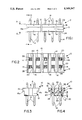
- FIG. 1 is a side elevational view of a header assembly embodying the concepts of the invention
- FIG. 2 is a top plan view of the header assembly
- FIG. 3 is an end elevational view of the header assembly
- FIG. 4 is a vertical section, on an enlarged scale and with the terminal pins in elevation, taken generally along line 4--4 of FIG. 1;
- FIG. 5 is a perspective view of an alternative embodiment of the present invention.
- FIG. 6 is a vertical section, on an enlarged scale and with the terminal pins in elevation, taken generally along line 6--6 of FIG. 5.
- the invention is embodied in a header assembly, generally designated 10, whichincludes an insulator block, generally designated 12, having a given thickness indicated by arrows "A" (FIG. 1), and a plurality of terminal pins 14 received in passages 20 (described hereinafter) in the insulator block.
- the first illustrated embodiment includes two rows of terminals pins in the insulator block but could include any desired number. To exemplify the miniaturization to which the invention is directed, the pinsare spaced apart 2.0 mm in each row, the rows are spaced 2.0 mm apart and each terminal pin is 0.50 mm in cross-dimensions such as the square pins shown.
- Insulator block 12 is unitarily molded of dielectric material such as plastic, or the like, and may be fabricated in a length which is longer than a desired length for a particular interconnection use. Specifically, insulator block 12 is shown in FIGS. 1 and 2 as being broken away at 15, representing that the block can be of a considerably greater length. Break-off grooves 16 are provided whereby the block, either before or after terminal pins 14 are mounted therein, can be broken into a particular length having a particular number of terminal pins for a particular interconnection application.
- insulator block 12 is provided with gripping means on the outside thereof to facilitate sliding the block off of terminal pins 14, as described hereinafter.
- the insulatorblock is provided with integral side flanges 18 projecting outwardly therefrom at the top thereof.
- the flanges define shoulders 18a on the underside thereof and under which gripping forces can be applied to lift the block off of terminal pins 14 in the direction of arrow "B".
- insulator block 12 is provided with a plurality of pin-receiving passages, generally designated 20, through the insulator block and extending between a top surface 22 and a bottom surface 24 of the block.
- Terminal pins 14 are inserted from the top into the through passages so that the pins project from bottom surface 24 for insertion into holes in a printed circuit board (not shown) and for solder connection to circuit traces on the board or in the holes.
- Each pin-receiving passage 20 is divided into three sections or areas, namely: a chamfered top area 26, a bottom interference-fit area 28 and a tapered area 30 between the top chamfered area and the bottom interference-fit area.
- the block 12 is thicker thanthe portion of the block that contacts the pins 14.
- a relatively thick block can be used which maintains the alignment of the pins to facilitate alignment and insertion with the appropriate holes in the printed circuit board yet still permit removal of the block after soldering.
- Top chamfered area 26 of each pin-receiving passage 20 is provided to define an enlarged mouth to facilitate inserting a pin into the respectivepassage during the manufacturing process.
- Tapered area 30 is provided for centering the pin upon further insertion of the pin into the passage.
- Interference-fit area 28 is provided to establish an interference-fit withthe terminal pin so that all of the terminal pins can be inserted into the holes in the printed circuit board by means of manipulating the insulator block, and thereafter to allow the block to be slid off the pins after thepins are soldered to the printed circuit board.
- the invention contemplates that interference-fitareas 28 between terminal pins 14 and the insulator block within pin-receiving passages 20 be less than the thickness "A" (FIG. 1) to reduce the amount of force required to slide the block off of the pins while still affording the block to be of a substantial thickness or size.
- the insulator block were only as thick as the interference-fit area 28, as indicated by double-headed arrows "C" (FIG. 4), the insulator block would be too thin to provide flanges 18 having anyrigidity and would likely be so flexible as to make alignment of all of thepins during insertion into the printed circuit board somewhat difficult.
- the design ofthe through passages in the insulator block enables a relatively rigid insulator block to be employed to fully protectthe terminal pins, to allow for the provision of gripping means such as flanges 18, and still reduce the amount of force required to remove the insulator block from the pins.
- the header assembly generally designated 40, includes an insulator block 42 having a given thickness "D" and a plurality of terminal pins 43 received in passages 44 in the insulator block.
- the insulator block 42 is provided with integral side flanges 46 that are similar to those shown in FIGS. 1-4 and serve the same purpose. Insulator block 42 is not shown as having break-off grooves, but such grooves could be provided if desired.
- each pin-receiving passage 44 includes a chamfered bottom area 52, a top interference-fit area 54 and a clearance area 56 in which the pin does not contact the passage between the chamfered bottom area and the top interference area.
- the width of top interference-fit area54 is designated as "E” and is substantially less than the thickness of block 42 which is designated "D".
- header assembly 40 is identical to that of header assembly 10 except that the pins are inserted into the passages 44 in insulator block 42 from the bottom past bottom surface 50.
- Insulator block 42 also includes stand-offs 58 for raising the insulator block 42 above the printed circuit board (not shown) to which the terminal pins 43 are soldered. After the pins are soldered to the board, block 42 is removed bygrasping flanges 46 and sliding the block upwards in the direction "F".
Landscapes
- Engineering & Computer Science (AREA)
- Manufacturing & Machinery (AREA)
- Manufacturing Of Electrical Connectors (AREA)
- Coupling Device And Connection With Printed Circuit (AREA)
Abstract
Description
Claims (11)
Priority Applications (4)
| Application Number | Priority Date | Filing Date | Title |
|---|---|---|---|
| US07/777,830 US5169347A (en) | 1991-10-15 | 1991-10-15 | Slip-off electrical connector header |
| JP4293700A JPH0650662B2 (en) | 1991-10-15 | 1992-10-07 | Slip-off electrical connector header |
| EP92117350A EP0541965A1 (en) | 1991-10-15 | 1992-10-10 | Slip-off electrical connector header |
| KR1019920018875A KR930009163A (en) | 1991-10-15 | 1992-10-14 | Slip off electrical splicer header |
Applications Claiming Priority (1)
| Application Number | Priority Date | Filing Date | Title |
|---|---|---|---|
| US07/777,830 US5169347A (en) | 1991-10-15 | 1991-10-15 | Slip-off electrical connector header |
Publications (1)
| Publication Number | Publication Date |
|---|---|
| US5169347A true US5169347A (en) | 1992-12-08 |
Family
ID=25111429
Family Applications (1)
| Application Number | Title | Priority Date | Filing Date |
|---|---|---|---|
| US07/777,830 Expired - Fee Related US5169347A (en) | 1991-10-15 | 1991-10-15 | Slip-off electrical connector header |
Country Status (4)
| Country | Link |
|---|---|
| US (1) | US5169347A (en) |
| EP (1) | EP0541965A1 (en) |
| JP (1) | JPH0650662B2 (en) |
| KR (1) | KR930009163A (en) |
Cited By (16)
| Publication number | Priority date | Publication date | Assignee | Title |
|---|---|---|---|---|
| US5242311A (en) * | 1993-02-16 | 1993-09-07 | Molex Incorporated | Electrical connector header with slip-off positioning cover and method of using same |
| US5281942A (en) * | 1991-06-21 | 1994-01-25 | Motorola Lighting, Inc. | Bobbin for an electrical winding and method of manufacture |
| US5340319A (en) * | 1992-08-07 | 1994-08-23 | Molex Incorporated | Electric connector for printed circuit boards |
| US5373626A (en) * | 1993-01-06 | 1994-12-20 | Elco Corporation | Removable pin carrier |
| US5439400A (en) * | 1993-07-01 | 1995-08-08 | Methode Electronics, Inc. | Disposable electrical connector header |
| US5579987A (en) * | 1992-02-18 | 1996-12-03 | Samsung Electronics Co., Ltd. | Semiconductor package vertical mounting device and mounting method |
| US5588849A (en) * | 1994-10-18 | 1996-12-31 | The Whitaker Corporation | Connector with pin terminals adapted for surface mounting |
| US5794336A (en) * | 1995-03-30 | 1998-08-18 | Thomas & Betts Corporation | Electrical connector having improved contact retention means |
| US5833498A (en) * | 1995-12-28 | 1998-11-10 | Berg Technology, Inc. | Electrical connector having improved retention feature and receptacle for use therein |
| US5964596A (en) * | 1998-02-02 | 1999-10-12 | Samtec, Inc. | Removable body for an electrical connector |
| US20040064164A1 (en) * | 2002-09-30 | 2004-04-01 | Ries Andrew J. | Connector module jumper for quadrapolar leads |
| US20040115997A1 (en) * | 2002-12-12 | 2004-06-17 | 3M Innovative Properties Company | Connector assembly |
| US20040209495A1 (en) * | 2002-12-06 | 2004-10-21 | Autosplice Systems Inc. | Solder reserve transfer device and process |
| US20060078216A1 (en) * | 2004-09-30 | 2006-04-13 | Fuji Photo Film Co., Ltd. | Image correction apparatus, method and program |
| US20120202371A1 (en) * | 2009-10-06 | 2012-08-09 | Phonak Ag | Integral connector for programming a hearing device |
| US9320151B2 (en) | 2011-10-17 | 2016-04-19 | General Electric Company | Protective sleeve for electrical components |
Families Citing this family (3)
| Publication number | Priority date | Publication date | Assignee | Title |
|---|---|---|---|---|
| ES1038860Y (en) * | 1997-11-25 | 1999-01-16 | Mecanismos Aux Ind | CONNECTOR FOR PINS FOR ELECTRONIC USE INTEGRATED IN PRINTED CIRCUITS. |
| US9960507B1 (en) * | 2017-04-28 | 2018-05-01 | Corning Optical Communications Rf Llc | Radio frequency (RF) connector pin assembly |
| US10199753B2 (en) | 2017-04-28 | 2019-02-05 | Corning Optical Communications Rf Llc | Multi-pin connector block assembly |
Citations (5)
| Publication number | Priority date | Publication date | Assignee | Title |
|---|---|---|---|---|
| US3545606A (en) * | 1968-06-11 | 1970-12-08 | Benny Morris Bennett | Flexible tape terminal assembly |
| US4061405A (en) * | 1974-09-09 | 1977-12-06 | Minter Jerry B | Apparatus for handling connectors |
| US4475284A (en) * | 1982-06-03 | 1984-10-09 | Teradyne, Inc. | Contact pin assembly tool |
| US4655517A (en) * | 1985-02-15 | 1987-04-07 | Crane Electronics, Inc. | Electrical connector |
| US5076796A (en) * | 1990-11-19 | 1991-12-31 | Molex Incorporated | Terminal pin for soldering to a printed circuit board |
Family Cites Families (5)
| Publication number | Priority date | Publication date | Assignee | Title |
|---|---|---|---|---|
| JPS593836A (en) * | 1982-06-29 | 1984-01-10 | 松下電工株式会社 | Device for starting discharge lamp |
| FR2561851B1 (en) * | 1984-03-26 | 1986-09-19 | Thomas & Betts Corp | DIVIDABLE BAR FOR HOLDING, LAYING ACCORDING TO A DETERMINED STEP, AND PROTECTION OF CONTACTS, PARTICULARLY FEMALE CONTACTS, TO BE WELDED ON A PRINTED CIRCUIT BOARD |
| JPH0537435Y2 (en) * | 1988-01-27 | 1993-09-21 | ||
| JPH034667U (en) * | 1989-06-07 | 1991-01-17 | ||
| JP3004667U (en) * | 1994-05-26 | 1994-11-22 | 能樹 羅 | Equipment for removing iron scraps generated during machining |
-
1991
- 1991-10-15 US US07/777,830 patent/US5169347A/en not_active Expired - Fee Related
-
1992
- 1992-10-07 JP JP4293700A patent/JPH0650662B2/en not_active Expired - Lifetime
- 1992-10-10 EP EP92117350A patent/EP0541965A1/en not_active Withdrawn
- 1992-10-14 KR KR1019920018875A patent/KR930009163A/en not_active Application Discontinuation
Patent Citations (5)
| Publication number | Priority date | Publication date | Assignee | Title |
|---|---|---|---|---|
| US3545606A (en) * | 1968-06-11 | 1970-12-08 | Benny Morris Bennett | Flexible tape terminal assembly |
| US4061405A (en) * | 1974-09-09 | 1977-12-06 | Minter Jerry B | Apparatus for handling connectors |
| US4475284A (en) * | 1982-06-03 | 1984-10-09 | Teradyne, Inc. | Contact pin assembly tool |
| US4655517A (en) * | 1985-02-15 | 1987-04-07 | Crane Electronics, Inc. | Electrical connector |
| US5076796A (en) * | 1990-11-19 | 1991-12-31 | Molex Incorporated | Terminal pin for soldering to a printed circuit board |
Cited By (21)
| Publication number | Priority date | Publication date | Assignee | Title |
|---|---|---|---|---|
| US5281942A (en) * | 1991-06-21 | 1994-01-25 | Motorola Lighting, Inc. | Bobbin for an electrical winding and method of manufacture |
| US5579987A (en) * | 1992-02-18 | 1996-12-03 | Samsung Electronics Co., Ltd. | Semiconductor package vertical mounting device and mounting method |
| US5340319A (en) * | 1992-08-07 | 1994-08-23 | Molex Incorporated | Electric connector for printed circuit boards |
| US5373626A (en) * | 1993-01-06 | 1994-12-20 | Elco Corporation | Removable pin carrier |
| US5242311A (en) * | 1993-02-16 | 1993-09-07 | Molex Incorporated | Electrical connector header with slip-off positioning cover and method of using same |
| US5439400A (en) * | 1993-07-01 | 1995-08-08 | Methode Electronics, Inc. | Disposable electrical connector header |
| US5588849A (en) * | 1994-10-18 | 1996-12-31 | The Whitaker Corporation | Connector with pin terminals adapted for surface mounting |
| US5794336A (en) * | 1995-03-30 | 1998-08-18 | Thomas & Betts Corporation | Electrical connector having improved contact retention means |
| US6033267A (en) * | 1995-12-28 | 2000-03-07 | Berg Technology, Inc. | Electrical connector having improved retention feature and receptacle for use therein |
| US5833498A (en) * | 1995-12-28 | 1998-11-10 | Berg Technology, Inc. | Electrical connector having improved retention feature and receptacle for use therein |
| US5964596A (en) * | 1998-02-02 | 1999-10-12 | Samtec, Inc. | Removable body for an electrical connector |
| US20040064164A1 (en) * | 2002-09-30 | 2004-04-01 | Ries Andrew J. | Connector module jumper for quadrapolar leads |
| US20040209495A1 (en) * | 2002-12-06 | 2004-10-21 | Autosplice Systems Inc. | Solder reserve transfer device and process |
| US6976855B2 (en) * | 2002-12-06 | 2005-12-20 | Auto Splice Systems Inc. | Solder reserve transfer device and process |
| US20040115997A1 (en) * | 2002-12-12 | 2004-06-17 | 3M Innovative Properties Company | Connector assembly |
| US6780069B2 (en) | 2002-12-12 | 2004-08-24 | 3M Innovative Properties Company | Connector assembly |
| US20060078216A1 (en) * | 2004-09-30 | 2006-04-13 | Fuji Photo Film Co., Ltd. | Image correction apparatus, method and program |
| US7286703B2 (en) * | 2004-09-30 | 2007-10-23 | Fujifilm Corporation | Image correction apparatus, method and program |
| US20120202371A1 (en) * | 2009-10-06 | 2012-08-09 | Phonak Ag | Integral connector for programming a hearing device |
| US8651895B2 (en) * | 2009-10-06 | 2014-02-18 | Phonak Ag | Integral connector for programming a hearing device |
| US9320151B2 (en) | 2011-10-17 | 2016-04-19 | General Electric Company | Protective sleeve for electrical components |
Also Published As
| Publication number | Publication date |
|---|---|
| KR930009163A (en) | 1993-05-22 |
| JPH05217657A (en) | 1993-08-27 |
| JPH0650662B2 (en) | 1994-06-29 |
| EP0541965A1 (en) | 1993-05-19 |
Similar Documents
| Publication | Publication Date | Title |
|---|---|---|
| US5169347A (en) | Slip-off electrical connector header | |
| US5242311A (en) | Electrical connector header with slip-off positioning cover and method of using same | |
| US5498167A (en) | Board to board electrical connectors | |
| US5681174A (en) | Electrical connector with releasable positioning cover | |
| US5320541A (en) | Electrical connector having terminals which cooperate with the edge of a circuit board | |
| US7927144B2 (en) | Electrical connector with interlocking plates | |
| US4159158A (en) | Displation connector having improved terminal supporting means | |
| KR970000122B1 (en) | Multi-conductor electrical connector and stamped and formed contacts for use therewith | |
| CA1240747A (en) | Electrical connector | |
| US4231628A (en) | Electrical connector receptacles | |
| US4188086A (en) | Connector for terminating flexible parallel conductors | |
| KR100192624B1 (en) | Electrical connector terminal and method of making electrical connector with the same | |
| US4417777A (en) | Integrated circuit carrier assembly | |
| US5644839A (en) | Surface mountable substrate edge terminal | |
| WO2011019572A2 (en) | Electrical connector system | |
| US4354718A (en) | Dual-in-line package carrier and socket assembly | |
| KR970702596A (en) | Low Profile Electrical Connector | |
| JPS5854474B2 (en) | Connector assembly for leadless integrated circuit package | |
| JPH07282888A (en) | Electric connector assembly | |
| US4655516A (en) | Chip carrier connector and method of making same | |
| KR970001944B1 (en) | Connector with press-fit terminal pins | |
| US5415560A (en) | Test clip for IC device | |
| US4380119A (en) | Method of making an electrical connector assembly | |
| US5439400A (en) | Disposable electrical connector header | |
| US7850489B1 (en) | Electrical connector system |
Legal Events
| Date | Code | Title | Description |
|---|---|---|---|
| AS | Assignment |
Owner name: MOLEX INCORPORATED, A CORP. OF DE, ILLINOIS Free format text: ASSIGNMENT OF ASSIGNORS INTEREST.;ASSIGNOR:SANG, LAI MAN;REEL/FRAME:005884/0582 Effective date: 19911009 |
|
| FPAY | Fee payment |
Year of fee payment: 4 |
|
| FEPP | Fee payment procedure |
Free format text: PAYOR NUMBER ASSIGNED (ORIGINAL EVENT CODE: ASPN); ENTITY STATUS OF PATENT OWNER: LARGE ENTITY |
|
| FPAY | Fee payment |
Year of fee payment: 8 |
|
| REMI | Maintenance fee reminder mailed | ||
| LAPS | Lapse for failure to pay maintenance fees | ||
| STCH | Information on status: patent discontinuation |
Free format text: PATENT EXPIRED DUE TO NONPAYMENT OF MAINTENANCE FEES UNDER 37 CFR 1.362 |
|
| FP | Lapsed due to failure to pay maintenance fee |
Effective date: 20041208 |