US6904112B1 - Method for modulating a basic clock signal for digital circuits and clock modulator for implementing the method - Google Patents
Method for modulating a basic clock signal for digital circuits and clock modulator for implementing the method Download PDFInfo
- Publication number
- US6904112B1 US6904112B1 US09/617,450 US61745000A US6904112B1 US 6904112 B1 US6904112 B1 US 6904112B1 US 61745000 A US61745000 A US 61745000A US 6904112 B1 US6904112 B1 US 6904112B1
- Authority
- US
- United States
- Prior art keywords
- delay
- clock signal
- random number
- switching edges
- delay units
- Prior art date
- Legal status (The legal status is an assumption and is not a legal conclusion. Google has not performed a legal analysis and makes no representation as to the accuracy of the status listed.)
- Expired - Lifetime, expires
Links
Images


Classifications
-
- H—ELECTRICITY
- H03—ELECTRONIC CIRCUITRY
- H03K—PULSE TECHNIQUE
- H03K5/00—Manipulating of pulses not covered by one of the other main groups of this subclass
- H03K5/13—Arrangements having a single output and transforming input signals into pulses delivered at desired time intervals
-
- G—PHYSICS
- G06—COMPUTING OR CALCULATING; COUNTING
- G06F—ELECTRIC DIGITAL DATA PROCESSING
- G06F1/00—Details not covered by groups G06F3/00 - G06F13/00 and G06F21/00
- G06F1/04—Generating or distributing clock signals or signals derived directly therefrom
- G06F1/10—Distribution of clock signals, e.g. skew
-
- H—ELECTRICITY
- H03—ELECTRONIC CIRCUITRY
- H03K—PULSE TECHNIQUE
- H03K5/00—Manipulating of pulses not covered by one of the other main groups of this subclass
- H03K5/13—Arrangements having a single output and transforming input signals into pulses delivered at desired time intervals
- H03K5/131—Digitally controlled
-
- H—ELECTRICITY
- H04—ELECTRIC COMMUNICATION TECHNIQUE
- H04B—TRANSMISSION
- H04B15/00—Suppression or limitation of noise or interference
- H04B15/02—Reducing interference from electric apparatus by means located at or near the interfering apparatus
- H04B15/04—Reducing interference from electric apparatus by means located at or near the interfering apparatus the interference being caused by substantially sinusoidal oscillations, e.g. in a receiver or in a tape-recorder
-
- H—ELECTRICITY
- H04—ELECTRIC COMMUNICATION TECHNIQUE
- H04B—TRANSMISSION
- H04B2215/00—Reducing interference at the transmission system level
- H04B2215/064—Reduction of clock or synthesizer reference frequency harmonics
-
- H—ELECTRICITY
- H04—ELECTRIC COMMUNICATION TECHNIQUE
- H04B—TRANSMISSION
- H04B2215/00—Reducing interference at the transmission system level
- H04B2215/064—Reduction of clock or synthesizer reference frequency harmonics
- H04B2215/067—Reduction of clock or synthesizer reference frequency harmonics by modulation dispersion
Definitions
- the invention relates to a method for modulating a basic clock signal for digital circuits and a clock modulator for modulating a basic clock signal for digital circuits.
- Modulation of the basic clock signal is used in order to give interference caused by the basic clock signal a broader-band configuration and thus to distribute the interference energy between additional frequencies and hence to reduce the absolute heights of the resulting interference spikes.
- the object of the invention is to provide a method for the frequency modulation of a basic clock signal which outputs a modulated clock signal which is identical on average to the basic clock signal, and a corresponding clock modulator for implementing the method.
- the object is achieved for a method the delay times of the delay units are calibrated, the delay units each having a plurality of delay elements and the delay elements being connected in or out individually and/or in groups. This makes it possible to compensate for effects such as, for example, current operating temperatures, changes in the voltage supply and ageing-dictated changes.
- This calibration is configured in a particularly simple manner if the delay elements are connected in or out in a stepwise approximated manner.
- This calibration can be carried out particularly rapidly and with always the same number of steps if firstly, during a coarse calibration, the same number of delay elements is connected in or out in each case in all the delay units and then, in a fine calibration, a respective delay element in one or more delay units is connected in or out.
- One manner of determining the distances between the switching edges may be realized by cyclically recurring random numbers, from which the respective distance is derived.
- the selection of the random numbers becomes particularly simple if the random numbers are inverted after n cycles for n cycles and the inverted numbers are then used for deriving the switching edges.
- the effect achieved as a result of this is that even given an unfavorable selection of the random numbers used, the modulated frequency on average corresponds to the fundamental frequency. This makes it possible, for example, to use the modulated frequency to provide an accurate time base for a clock, for example.
- the switching edges are derived not only as a function of the random number but also as a function of a modulation factor, it is possible to realize different modulation factors.
- One manner of determination of the next switching edge can be implemented by the formula specified herein. This makes it possible to freely select the modulation factor, the number of delay elements and of different random numbers or switching edges within the scope of the physical limits of the clock signal to be modulated and of the switching device.
- a clock modulator has a number of series-connected delay units with adjustable delay times between which taps are arranged, so that the basic clock signal can be conducted via a changing number of delay units and the distance between the switching edges can be altered in this way, the adjustability of the delay units being realized by virtue of the fact that the delay units are each constructed from a plurality of delay elements which can be connected and disconnected individually.
- the clock modulator can be used for different fundamental frequencies and modulation factors.
- the selection of the random numbers becomes simple by virtue of an inverting device for inverting the random numbers.
- This inverting device can be connected in after n cycles of the random numbers and can be disconnected again after a further n cycles.
- the random numbers are inverted, the inverted random numbers, instead of the random numbers, are used for deriving the distances between adjacent switching edges.
- the effect achieved as a result of this is that the average clock duration of the modulated frequency is equal to the duration of the modulated basic clock signal, irrespective of the selection of the random numbers.
- FIG. 1 shows a diagram containing the basic clock signal and the generation of the modulated clock signal
- FIG. 2 shows a block diagram of a possible exemplary embodiment
- FIG. 3 shows an exemplary embodiment of a particularly preferred clock modulator
- FIG. 4 shows a function diagram of the exemplary embodiment of FIG. 3 .
- FIG. 5 shows a block diagram of an exemplary embodiment of a delay unit
- FIG. 6 shows a possibility for approximated calibration of series-connected delay units.
- a random number generator supplies 5 different random numbers Z 0 to 4 in periodic cycles.
- the distances between the individual switching edges of the clock signal to be modulated are determined depending on the random number Z and the modulation factor K.
- the distance between the adjacent switching edges amounts to a half-period T 0 .
- the following distances between the switching edges result for the remaining random numbers.
- FIG. 2 For block diagram of an exemplary embodiment of the clock modulator according to the invention in FIG. 2 has n series-connected delay units D 1 to D n with upstream and downstream taps A 0 to A n connected to a multiplexer 1 .
- a calibrating device 2 compares the basic clock signal CL present at the input E with the signal present at the output A n of the last delay element D n . If the instants of the switching edges of the two signals do not correspond, the calibrating device 2 calibrates the delay units D 1 to D n in such a way that the two signals correspond.
- m random numbers are generated cyclically with the aid of a feedback shift register 3 .
- Different random number sequences can be selected by means of an initialization device 4 .
- the random numbers read from the feedback shift register are inverted by an inverter 5 , in order to obtain uniform distribution of the random numbers and thus of the different delays. If there are an even number of different random numbers, said number is reduced by one in a map device 6 , thereby producing an odd number of different random numbers. This reduction can be realized for example as follows: when the highest random number is present, it is not taken, rather the remaining random numbers are taken one after the other. This can be done for example as follows: when said highest random number is present, a counter which counts from zero up to the highest random number still allowed is read and is then incremented by one.
- the random numbers thus obtained are used, as described above with reference to FIG. 1 , in the arithmetic unit 7 in order to determine the tap A 0 to A n to which the multiplexer 1 must be switched so that the switching edge corresponding to the random number and to the modulation factor is obtained.
- delay units D 1 -D 7 are connected in series to form a delay chain via which the basic clock signal CLK is conducted.
- the basic clock signal CLK (corresponding to the signal TAPP 0 ) and the signals TAPP 1 -P 3 which leave the delay units D 1 -D 3 are respectively present at an input 20 a - d of a multiplexer 20 , and the signals TAP N 0 -N 3 which leave the delay units D 4 -D 7 are present at a respective input 20 a - d of the multiplexer 21 .
- the outputs of the multiplexers 20 , 21 are connected to the inputs of a multiplexer 22 , whose output is connected to the input of a toggle flip-flop 23 , at whose output the modulated clock signal f MOD is present.
- the signals TAPP 0 -TAPP 3 are also passed to a calibrating unit 24 , which monitors whether the delay of said signals is correct. If this is not the case, the delay units D 1 -D 4 are calibrated until the delay is correct.
- the values determined for delay units D 1 -D 4 are also accepted for the delay units D 5 to D 7 , since they have the same operating parameters as the delay units D 1 -D 4 , particularly if all the delay units D 1 -D 7 or even the entire clock modulator are integrated in an IC.
- This calibration may be effected continually or at specific time intervals or, by way of example, may be carried out in the event of changes in specific parameters such as, for example, temperature or circuit.
- FIG. 3 furthermore shows a multiplier 25 , two adders 26 , 27 , a register 28 , a toggle flip-flop 29 , a lock flip-flop 30 and a random number generator 31 .
- the next random number Z i+1 is present at the input 25 a
- the modulation factor K is present at the input 25 b
- the constant c is present at the input 26 a
- the position a i of the preceding switching edge SF, which is read from the register 28 is present at the input 26 b.
- the product from the multiplier 25 and the sum from the adder 26 are summed in the adder 27 to give a sum S.
- the highest bit of this sum S is passed to the set input of the lock flip-flop 30
- the second highest bit is passed to the input of the toggle flip-flop 29
- the two remaining, lower bits are passed to the register 28 .
- the output of the register 28 drives the two multiplexers 20 , 21 and is furthermore fed back to an input of the adder 26 .
- FIG. 4 shows an exemplary illustration of the method of operation of the above-described clock modulator in the form of a diagram.
- TAPP 0 to TAPP 3 denote the signals which are present at the inputs of the multiplexer 20
- TAPN 0 to N 3 the signals which are present at the inputs of the multiplexer 21 .
- LB denotes the number produced by the lowest two bits of the sum S and thus represents the number of the signal TAPP 0 -TAPP 3 and TAPN 0 -TAPN 3
- Z i denotes the random number which is present in each case
- UB denotes the number of the two upper bits of the sum S
- INT denotes the output of the toggle flip-flop 29
- LOCK denotes the output of the lock flip-flop 30 .
- the 3 means that the input TAPP 3 and respectively TAPN 3 of the multiplexer 21 is switched through, with the result that the signal which is present downstream of the delay unit D 3 is switched through, which signal, upon its next positive edge, will switch over the output of the toggle flip-flop 23 .
- FIG. 5 reveals the possible structure of a delay unit D.
- the delay unit D comprises m series-connected delay elements 10 .
- the delay elements 10 each have a clock input 11 , two clock outputs 12 , 13 and a control input 14 .
- the respective clock output 12 is connected to the output 14 of the delay unit D, while the respective clock output 13 is connected to the clock input 11 of the respectively succeeding delay element 10 .
- the control inputs 14 determine the clock output 12 , 13 at which the (delayed) clock signal is present and thus whether the clock signal is to be delayed further or is to pass undelayed to the output 14 . Consequently, the delay time of each delay unit D can be varied in a wide range.
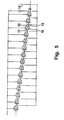
- the timing diagram in FIG. 6 shows one possibility for approximated calibration of the delay units from FIG. 3 .
- the same number of delay elements are used in each delay unit D 1 -D 4 in order to delay the clock signal CL. Since the clock signal is delayed by more than one complete half-period in the case of the delay unit D 4 , an identical number of delay elements are in each case connected out in the delay units D 1 -D 4 . This is carried out in a plurality of steps with a decreasing number until, by connecting in or out a respective delay element in each delay unit, the clock signal is delayed by almost half a period in the case of the delay unit D 4 and the end E of the coarse calibration is reached.
- the delay units D 5 -D 7 are then set in a corresponding manner.
Landscapes
- Engineering & Computer Science (AREA)
- Physics & Mathematics (AREA)
- Nonlinear Science (AREA)
- Theoretical Computer Science (AREA)
- Computer Networks & Wireless Communication (AREA)
- Signal Processing (AREA)
- General Engineering & Computer Science (AREA)
- General Physics & Mathematics (AREA)
- Pulse Circuits (AREA)
Abstract
Description
- 0=4t
- 1=5t
- 3=7t
- 4=8t
- 0=2t
- 1=4t
- 3=8t
- 4=10t
x=I*p+ax*t
where I is the interval in which the next switching edge lies, p is the number of possible switching points per half-period T0 and a is the position of the switching edge in the corresponding interval.
a i+1=(0+6−(5−I/2−1)×1)mod6=5mod6
5=I*6+5*1
from this it follows that:
I=0 a=5
a i+1=(5+6−(5−I/2−4)×1)mod6=13mod6
13=I*6+a*1
I=1 a=1
a i+1=(1+6−(5−I/2−2)×1)mod6=7mod6
7=I*6+a*1
I=1 a=1
a i+1=(1+6−(5−I/2−0)×1)mod6=5mod6
5=I*6+a*1
I=0 a=5
a i+1=(0+6−(5−I/2−1)×2)mod6=4mod6
4=I*6+a*1
I=0 a=4
a i+1=(4+6−(5−I/2−4)×2)mod6=14mod6
14=I*6+a*1
I=2 a=2
a i+1=(2+6−(5−I/2−2)×2)mod6=8mod6
6=I*6+a*1
I=1 a=2
a i+1=(2+6−(5−I/2−0)×2)mod6=4mod6
4=I*6+a*1
I=0 a=4
S=a i+1=(a i +K*Z i+1 +c)modp
where c=p−((N−1):2)*K
| | LB | ||
| 3 | 00 | 11 |
| 4 | 01 | 00 |
| 5 | 01 | 01 |
| 6 | 01 | 10 |
| 7 | 01 | 11 |
| 8 | 10 | 00 |
S=3+1×1+3=7 or, in binary, 0 1 1 1
is accepted into the
Claims (2)
Applications Claiming Priority (1)
| Application Number | Priority Date | Filing Date | Title |
|---|---|---|---|
| DE19933115A DE19933115A1 (en) | 1999-07-19 | 1999-07-19 | Method for modulating a basic clock for digital circuits and clock modulator for carrying out the method |
Publications (1)
| Publication Number | Publication Date |
|---|---|
| US6904112B1 true US6904112B1 (en) | 2005-06-07 |
Family
ID=7914851
Family Applications (1)
| Application Number | Title | Priority Date | Filing Date |
|---|---|---|---|
| US09/617,450 Expired - Lifetime US6904112B1 (en) | 1999-07-19 | 2000-07-17 | Method for modulating a basic clock signal for digital circuits and clock modulator for implementing the method |
Country Status (4)
| Country | Link |
|---|---|
| US (1) | US6904112B1 (en) |
| EP (1) | EP1071208B1 (en) |
| JP (1) | JP4597326B2 (en) |
| DE (2) | DE19933115A1 (en) |
Cited By (3)
| Publication number | Priority date | Publication date | Assignee | Title |
|---|---|---|---|---|
| US20040183469A1 (en) * | 2001-01-09 | 2004-09-23 | Yung-Lin Lin | Sequential burnst mode activation circuit |
| US7103622B1 (en) * | 2002-10-08 | 2006-09-05 | Analog Devices, Inc. | Direct digital synthesizer with output signal jitter reduction |
| US20070194817A1 (en) * | 2006-02-22 | 2007-08-23 | Analog Devices, Inc. | Spread-spectrum clocking |
Families Citing this family (3)
| Publication number | Priority date | Publication date | Assignee | Title |
|---|---|---|---|---|
| US6507247B2 (en) * | 2001-02-27 | 2003-01-14 | Corrent Corporation | Circuit and method for generating a variable frequency clock signal |
| DE10249886B4 (en) * | 2002-10-25 | 2005-02-10 | Sp3D Chip Design Gmbh | Method and apparatus for generating a clock signal having predetermined clocking characteristics |
| KR100856123B1 (en) * | 2006-03-20 | 2008-09-03 | 삼성전자주식회사 | Data processing apparatus and method for reducing EMI emission |
Citations (19)
| Publication number | Priority date | Publication date | Assignee | Title |
|---|---|---|---|---|
| US4933890A (en) | 1989-06-13 | 1990-06-12 | The Charles Stark Draper Laboratory, Inc. | Digital frequency synthesizer |
| US5252867A (en) | 1992-02-14 | 1993-10-12 | Vlsi Technology, Inc. | Self-compensating digital delay semiconductor device with selectable output delays and method therefor |
| DE4423186A1 (en) | 1993-07-01 | 1995-01-19 | Teradyne Inc | Method and device for testing integrated circuits |
| US5471165A (en) | 1993-02-24 | 1995-11-28 | Telefonaktiebolaget Lm Ericsson | Signal processing circuit and a method of delaying a binary periodic input signal |
| DE4442403A1 (en) | 1994-11-30 | 1996-09-05 | Itt Ind Gmbh Deutsche | Clock generator for generating a low-interference system clock |
| DE19517265A1 (en) | 1995-05-11 | 1996-11-14 | Vdo Schindling | Interference reduction method esp. for timing signal controlled devices |
| DE19546805A1 (en) | 1995-07-14 | 1997-01-16 | Lg Semicon Co Ltd | Pulse width modulation circuit |
| EP0828360A1 (en) | 1996-09-04 | 1998-03-11 | Micronas Intermetall GmbH | Clock generator for producing a low noise system clock |
| US5777501A (en) | 1996-04-29 | 1998-07-07 | Mosaid Technologies Incorporated | Digital delay line for a reduced jitter digital delay lock loop |
| US5789958A (en) | 1997-01-13 | 1998-08-04 | Credence Systems Corporation | Apparatus for controlling timing of signal pulses |
| US5805616A (en) * | 1994-11-10 | 1998-09-08 | Samsung Electronics, Co., Ltd. | Circuit of calculating errata locator and evaluator polynomial, calculating method thereof and reed-solomon decoder using the same |
| WO1998058449A2 (en) | 1997-06-18 | 1998-12-23 | Credence Systems Corporation | Programmable delay circuit having calibratable delays |
| DE19802065A1 (en) | 1998-01-21 | 1999-07-22 | Mannesmann Vdo Ag | Clock modulator for controlling microprocessors and / or other digital circuits |
| US5945862A (en) * | 1997-07-31 | 1999-08-31 | Rambus Incorporated | Circuitry for the delay adjustment of a clock signal |
| US6040726A (en) * | 1998-09-14 | 2000-03-21 | Lucent Technologies Inc. | Digital duty cycle correction loop apparatus and method |
| US6065127A (en) * | 1998-09-14 | 2000-05-16 | Globespan Semiconductor, Inc. | Multi-mode buffer for digital signal processor |
| US6259467B1 (en) * | 1999-02-09 | 2001-07-10 | International Business Machines Corporation | Multi stage oscillator phase alignment scheme |
| US6390579B1 (en) * | 1999-04-15 | 2002-05-21 | Hewlett-Packard Company | Pulse width modulator using delay-line technology with automatic calibration of delays to desired operating frequency |
| US6400735B1 (en) * | 1998-06-22 | 2002-06-04 | Xilinx, Inc. | Glitchless delay line using gray code multiplexer |
Family Cites Families (6)
| Publication number | Priority date | Publication date | Assignee | Title |
|---|---|---|---|---|
| JPS6263327A (en) * | 1985-09-13 | 1987-03-20 | Fujitsu Ten Ltd | Oscillation circuit of microcomputer |
| JP2576585B2 (en) * | 1988-04-30 | 1997-01-29 | 株式会社島津製作所 | Pulse generator |
| JPH02104124A (en) * | 1988-10-13 | 1990-04-17 | Matsushita Electric Ind Co Ltd | Pulse width modulation method |
| JPH05152908A (en) * | 1991-11-25 | 1993-06-18 | Nec Corp | Clock signal generating circuit |
| US5281874A (en) * | 1992-02-14 | 1994-01-25 | Vlsi Technology, Inc. | Compensated digital delay semiconductor device with selectable output taps and method therefor |
| US5442664A (en) * | 1993-12-20 | 1995-08-15 | Hewlett-Packard Company | Digitally phase modulated clock inhibiting reduced RF emissions |
-
1999
- 1999-07-19 DE DE19933115A patent/DE19933115A1/en not_active Ceased
-
2000
- 2000-07-03 EP EP00114213A patent/EP1071208B1/en not_active Expired - Lifetime
- 2000-07-03 DE DE50011544T patent/DE50011544D1/en not_active Expired - Lifetime
- 2000-07-17 US US09/617,450 patent/US6904112B1/en not_active Expired - Lifetime
- 2000-07-18 JP JP2000217479A patent/JP4597326B2/en not_active Expired - Lifetime
Patent Citations (21)
| Publication number | Priority date | Publication date | Assignee | Title |
|---|---|---|---|---|
| US4933890A (en) | 1989-06-13 | 1990-06-12 | The Charles Stark Draper Laboratory, Inc. | Digital frequency synthesizer |
| US5252867A (en) | 1992-02-14 | 1993-10-12 | Vlsi Technology, Inc. | Self-compensating digital delay semiconductor device with selectable output delays and method therefor |
| US5471165A (en) | 1993-02-24 | 1995-11-28 | Telefonaktiebolaget Lm Ericsson | Signal processing circuit and a method of delaying a binary periodic input signal |
| DE4423186A1 (en) | 1993-07-01 | 1995-01-19 | Teradyne Inc | Method and device for testing integrated circuits |
| US5805616A (en) * | 1994-11-10 | 1998-09-08 | Samsung Electronics, Co., Ltd. | Circuit of calculating errata locator and evaluator polynomial, calculating method thereof and reed-solomon decoder using the same |
| DE4442403A1 (en) | 1994-11-30 | 1996-09-05 | Itt Ind Gmbh Deutsche | Clock generator for generating a low-interference system clock |
| DE19517265A1 (en) | 1995-05-11 | 1996-11-14 | Vdo Schindling | Interference reduction method esp. for timing signal controlled devices |
| DE19546805A1 (en) | 1995-07-14 | 1997-01-16 | Lg Semicon Co Ltd | Pulse width modulation circuit |
| US5638017A (en) | 1995-07-14 | 1997-06-10 | Lg Semicon Co., Ltd. | Pulse width modulation circuit |
| US5777501A (en) | 1996-04-29 | 1998-07-07 | Mosaid Technologies Incorporated | Digital delay line for a reduced jitter digital delay lock loop |
| EP0828360A1 (en) | 1996-09-04 | 1998-03-11 | Micronas Intermetall GmbH | Clock generator for producing a low noise system clock |
| US5789958A (en) | 1997-01-13 | 1998-08-04 | Credence Systems Corporation | Apparatus for controlling timing of signal pulses |
| WO1998058449A2 (en) | 1997-06-18 | 1998-12-23 | Credence Systems Corporation | Programmable delay circuit having calibratable delays |
| US5945862A (en) * | 1997-07-31 | 1999-08-31 | Rambus Incorporated | Circuitry for the delay adjustment of a clock signal |
| DE19802065A1 (en) | 1998-01-21 | 1999-07-22 | Mannesmann Vdo Ag | Clock modulator for controlling microprocessors and / or other digital circuits |
| US6393078B1 (en) * | 1998-01-21 | 2002-05-21 | Mannesmann Vdo Ag | Clock modulator for driving microprocessors and/or other digital circuits |
| US6400735B1 (en) * | 1998-06-22 | 2002-06-04 | Xilinx, Inc. | Glitchless delay line using gray code multiplexer |
| US6040726A (en) * | 1998-09-14 | 2000-03-21 | Lucent Technologies Inc. | Digital duty cycle correction loop apparatus and method |
| US6065127A (en) * | 1998-09-14 | 2000-05-16 | Globespan Semiconductor, Inc. | Multi-mode buffer for digital signal processor |
| US6259467B1 (en) * | 1999-02-09 | 2001-07-10 | International Business Machines Corporation | Multi stage oscillator phase alignment scheme |
| US6390579B1 (en) * | 1999-04-15 | 2002-05-21 | Hewlett-Packard Company | Pulse width modulator using delay-line technology with automatic calibration of delays to desired operating frequency |
Cited By (9)
| Publication number | Priority date | Publication date | Assignee | Title |
|---|---|---|---|---|
| US20040183469A1 (en) * | 2001-01-09 | 2004-09-23 | Yung-Lin Lin | Sequential burnst mode activation circuit |
| US7477024B2 (en) * | 2001-01-09 | 2009-01-13 | O2Micro International Limited | Sequential burst mode activation circuit |
| US7847491B2 (en) | 2001-01-09 | 2010-12-07 | O2Micro International Limited | Sequential burst mode activation circuit |
| US7103622B1 (en) * | 2002-10-08 | 2006-09-05 | Analog Devices, Inc. | Direct digital synthesizer with output signal jitter reduction |
| US20070194817A1 (en) * | 2006-02-22 | 2007-08-23 | Analog Devices, Inc. | Spread-spectrum clocking |
| WO2007100529A3 (en) * | 2006-02-22 | 2007-11-15 | Analog Devices Inc | Spread-spectrum clocking |
| US7437590B2 (en) | 2006-02-22 | 2008-10-14 | Analog Devices, Inc. | Spread-spectrum clocking |
| JP2009527989A (en) * | 2006-02-22 | 2009-07-30 | アナログ・デバイシズ・インコーポレーテッド | Spread spectrum clocking |
| CN101411064B (en) * | 2006-02-22 | 2012-05-09 | 美国亚德诺半导体公司 | Method and device for generating spread spectrum clock signal |
Also Published As
| Publication number | Publication date |
|---|---|
| JP4597326B2 (en) | 2010-12-15 |
| EP1071208A2 (en) | 2001-01-24 |
| EP1071208B1 (en) | 2005-11-09 |
| DE50011544D1 (en) | 2005-12-15 |
| JP2001068979A (en) | 2001-03-16 |
| EP1071208A3 (en) | 2001-05-09 |
| DE19933115A1 (en) | 2001-01-25 |
Similar Documents
| Publication | Publication Date | Title |
|---|---|---|
| CN108336994B (en) | Clock synthesizer with integral nonlinearity interpolation (INL) distortion compensation | |
| US5719515A (en) | Digital delay line | |
| US9735787B2 (en) | Frequency synthesizer with dynamic phase and pulse-width control | |
| KR20100047217A (en) | System, method and apparatus having improved pulse width modulation frequency resolution | |
| WO2002031980A2 (en) | Cyclic phase signal generation from a single clock source using current phase interpolation | |
| US20050200393A1 (en) | Method and device for generating a clock signal with predetermined clock signal properties | |
| JPH03253108A (en) | Direct digital synthesizer and signal generation | |
| US6998893B2 (en) | Circuit and method for inducing jitter to a signal | |
| US6904112B1 (en) | Method for modulating a basic clock signal for digital circuits and clock modulator for implementing the method | |
| US5592659A (en) | Timing signal generator | |
| US7095264B2 (en) | Programmable jitter signal generator | |
| JP3524967B2 (en) | Timing generator for multiple reference oscillators | |
| JP3633988B2 (en) | Timing edge generation circuit for semiconductor IC test equipment | |
| US7312668B2 (en) | High resolution PWM generator or digitally controlled oscillator | |
| US6741660B1 (en) | Method for modulation of a basic clock for digital circuits, and a modulator for carrying out the method | |
| USRE36063E (en) | Timing generator with edge generators, utilizing programmable delays, providing synchronized timing signals at non-integer multiples of a clock signal | |
| US7733152B2 (en) | Control signal generating circuit enabling value of period of a generated clock signal to be set as the period of a reference signal multiplied or divided by an arbitrary real number | |
| RU2168268C1 (en) | Generator with separate digital phase and frequency control of pulses | |
| KR100807610B1 (en) | Frequency multiply circuit using smd, with arbitrary multiplication factor | |
| JP2000275309A (en) | Semiconductor device tester, timing generator, method for testing semiconductor device, and method for generating timing | |
| KR100202327B1 (en) | Timming generator for plural reference oscillator | |
| RU2259630C1 (en) | Device for automatic-phase control of pulse generator | |
| JP3060970B2 (en) | Pulse width modulation circuit | |
| US10763870B1 (en) | Digital fractional clock synthesizer with period modulation | |
| RU2223597C1 (en) | Digital frequency synthesizer |
Legal Events
| Date | Code | Title | Description |
|---|---|---|---|
| AS | Assignment |
Owner name: MANNESMANN VDO AG, GERMANY Free format text: ASSIGNMENT OF ASSIGNORS INTEREST;ASSIGNORS:SATTLER, DR. FRANK;KLUMB, WALTER;REEL/FRAME:011830/0751;SIGNING DATES FROM 20000927 TO 20001023 Owner name: FUJITSU MICROELECTRONICS EUROPE GMBH, GERMANY Free format text: ASSIGNMENT OF ASSIGNORS INTEREST;ASSIGNORS:SATTLER, DR. FRANK;KLUMB, WALTER;REEL/FRAME:011830/0751;SIGNING DATES FROM 20000927 TO 20001023 |
|
| STCF | Information on status: patent grant |
Free format text: PATENTED CASE |
|
| FPAY | Fee payment |
Year of fee payment: 4 |
|
| AS | Assignment |
Owner name: SIEMENS AKTIENGESELLSCHAFT, GERMANY Free format text: MERGER;ASSIGNOR:MANNESMANN VDO AKTIENGESELLSCHAFT;REEL/FRAME:026005/0303 Effective date: 20100315 |
|
| AS | Assignment |
Owner name: CONTINENTAL AUTOMOTIVE GMBH, GERMANY Free format text: ASSIGNMENT OF ASSIGNORS INTEREST;ASSIGNOR:SIEMENS AKTIENGESELLSCHAFT;REEL/FRAME:027263/0068 Effective date: 20110704 |
|
| FPAY | Fee payment |
Year of fee payment: 8 |
|
| FPAY | Fee payment |
Year of fee payment: 12 |