US6829694B2 - Reconfigurable parallel look up table system - Google Patents
Reconfigurable parallel look up table system Download PDFInfo
- Publication number
- US6829694B2 US6829694B2 US10/131,007 US13100702A US6829694B2 US 6829694 B2 US6829694 B2 US 6829694B2 US 13100702 A US13100702 A US 13100702A US 6829694 B2 US6829694 B2 US 6829694B2
- Authority
- US
- United States
- Prior art keywords
- look
- index register
- tables
- address
- values
- Prior art date
- Legal status (The legal status is an assumption and is not a legal conclusion. Google has not performed a legal analysis and makes no representation as to the accuracy of the status listed.)
- Expired - Lifetime, expires
Links
Images


Classifications
-
- G—PHYSICS
- G06—COMPUTING; CALCULATING OR COUNTING
- G06F—ELECTRIC DIGITAL DATA PROCESSING
- G06F9/00—Arrangements for program control, e.g. control units
- G06F9/06—Arrangements for program control, e.g. control units using stored programs, i.e. using an internal store of processing equipment to receive or retain programs
- G06F9/30—Arrangements for executing machine instructions, e.g. instruction decode
- G06F9/34—Addressing or accessing the instruction operand or the result ; Formation of operand address; Addressing modes
- G06F9/345—Addressing or accessing the instruction operand or the result ; Formation of operand address; Addressing modes of multiple operands or results
-
- G—PHYSICS
- G06—COMPUTING; CALCULATING OR COUNTING
- G06F—ELECTRIC DIGITAL DATA PROCESSING
- G06F12/00—Accessing, addressing or allocating within memory systems or architectures
- G06F12/02—Addressing or allocation; Relocation
- G06F12/0207—Addressing or allocation; Relocation with multidimensional access, e.g. row/column, matrix
Definitions
- This invention relates to a reconfigurable parallel look-up table system
- the invention results from the realization that a truly faster and more flexible look-up table system can be achieved by enabling a number of look-up tables in a memory to be accessed simultaneously by combining the values to be looked up with the values representing the starting addresses of the look-up tables to simultaneously translate each value into an address to locate in parallel the function of those values in each look-up table.
- This invention features a reconfigurable parallel look-up table system including a memory and a plurality of look-up tables stored on the memory.
- a row index register holds the values to be looked up in the look-up tables, and the column index register stores the value representing the starting address of each of the look-up tables stored in the memory.
- An address translation circuit is responsive to the column index register and the row index register to simultaneously generate an address for each value in the row index register to locate in parallel the functions of those values in each look-up table.
- the address translation circuit may include a multiplier circuit for multiplying the value representing the starting address by the length of each column and an adder circuit for combining the value in the row index register with the output of the multiplier circuit.
- the address translation circuit may include an OR circuit for combining the values from the row index register with the values in the column index register shifted toward the MSB by N bits in respect to the values in the row index register.
- the look-up tables may be all the same size.
- FIG. 1 is a simplified block diagram of a reconfigurable parallel look-up table system according to this invention
- FIG. 2 is a schematic diagram of a typical linear memory structure
- FIG. 3 is a schematic diagram illustrating the columns of FIG. 2 arranged in a side by side look-up table arrangement
- FIG. 4 is a simplified schematic diagram illustrating one approach to combining the row and column index register values to obtain an address for locating value functions in look-up tables
- FIG. 5 is a schematic diagram of the row and column index registers according to this invention to accomplish the address generation described in FIG. 4;
- FIG. 6 is a graphical illustration of the shifting and combination of the eight bits of information in each of the stages of the register of FIG. 5 showing the ultimate address generation effected;
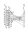
- FIG. 7 illustrates a sample of the number of different configurations of look-up tables that may be achieved with this invention
- FIG. 8 is a schematic diagram of one embodiment of a reconfigurable parallel look-up table according to this invention.
- FIG. 9 is a more detailed schematic diagram of one of the OR circuits of FIG. 8.
- FIGS. 10 and 11 are schematic diagrams showing two different configurations of parallel look-up tables that can be effected according to this invention.
- FIG. 1 a reconfigurable parallel look-up table system 10 according to this invention which includes a row index register R 2 , 12 and a column index register R 1 , 14 , an address translation circuit 16 and a memory 18 which contains a number of look-up tables.
- the output from memory 18 is delivered to output register 20 .
- Memory 18 includes a number of look-up tables and row index register 12 holds the values to be looked up in those look-up tables.
- row index register 12 may hold the angles that are to be looked up in the look-up tables at memory 18 where each of the look-up tables has a different function, one of the sine value, cosine value, tangent value, and so on for those angles.
- Column index register 14 stores a value representing the starting address of each look-up table stored in the memory. For example, if memory 18 holds eight look-up tables of 64 bytes each, the starting points for those look-up tables which coincide with the columns 30 , 32 , 34 , 36 , 38 , 40 , 42 , 44 will be 0 , 64 , 128 , 192 , 256 , 320 , 384 , and 448 .
- Address translation circuit 16 combines the value in the row index register 12 with a representation of the starting address of each of the look-up tables to simultaneously generate an address for each value in the index register to locate in parallel the function of those values in each look-up table.
- Memories are typically made in a linear fashion as shown in FIG. 3 for manufacturing convenience.
- a memory that has a storage capacity of 512 bytes each byte comprising eight bits will be constructed as indicated by memory 18 a , FIG. 2, where there are eight columns 30 - 44 running one after another and containing rows of bytes 0 - 63 , 64 - 127 , 128 - 191 , 192 - 255 , 256 - 319 , 320 - 383 , 384 - 447 , 448 - 511 .
- memory 18 a will more likely be envisioned as memory 18 b , FIG.
- each of the columns 30 - 44 are envisioned in side by side position each extending for sixty-four rows 46 , numbered 0 - 63 .
- the area to be addressed is in the fifth column and fourth row, namely shaded area 48 , this can be seen in FIG. 2 as the 324 th row in the 0 - 511 rows depicted there.
- the output of adder 52 will be 324 , precisely the address of location 48 shown as row 4 and column 5 in FIG. 3, also shown directly as address 324 in FIG. 2 .
- FIG. 5 where the row index register 12 b and the column index register 14 b are shown as eight stage registers, each stage representing a byte, each byte of 8bits.
- the first stage 60 resides the number four as previously, but in the first stage 62 of register 14 b resides the number forty, because this number will be multiplied by eight due to a hardwired shift of three bits to provide the number 320 as previously explained.
- FIG. 6 shows the eight bit structure with a “1” in the third bit position, 64 , representing binary four.
- Stage 62 of register 14 b is shown with its eight bits having a “1” in the fourth and sixth bit position where the “1” bit at 66 represents an eight and the “1” bit at 68 represents thirty-two for a total of forty.
- the eight bits from stage 62 of register 14 b have been shifted three bits to the left relative to the eight bits of stage 60 from register 12 b . This effectively multiplies by eight the value in stage 62 .
- reconfigurable parallel look-up system 1 O f FIG. 8 includes row index register 12 f and column index register 14 f , each of which have eight stages as explained previously with respect to FIG. 6 and a memory 18 f which includes eight columns of sixty-four bytes each as illustrated in FIG. 3 .
- the address translation circuit 16 f includes a number of OR circuits.
- One OR circuit is associated with each pair of stages from each of registers 12 f and 14 f . There are thus eight OR circuits, only three of which are shown for clarity, 90 , 92 and 94 .
- OR circuit 90 receives five of the eight inputs from eight bit stage 60 f , while the three remaining least significant bits from stage 60 are delivered directly to the memory address bus 96 .
- the other inputs to OR gate 90 are six bits from the first stage 62 f of register 14 f . These are combined as explained with respect to FIG. 6 so that the five bits from stage 60 f and the six bits from the shifted stage 62 f are OR-ed to produce a six bit output which is then combined with the three least significant bits from stage 60 f to provide the nine bit address on address bus 96 .
- OR circuits 92 and 94 and the other OR circuits omitted for clarity operate in the same way to address locations in memory 18 f.
- Each OR circuit as exemplified by OR circuit 90 , FIG. 9 includes five OR gates, 100 , 102 , 104 , 106 and 108 which combine the bits from the third, fourth, fifth, sixth and seventh positions of stage 60 f with those from positions zero, one, two, three, and four of stage 62 f , respectively, with the bits in stage 62 having been shifted by three places with respect to those in stage 60 f .
- the first three bits zero, one, two of stage 60 f are delivered directly, not through OR gates, to provide the nine bit address zero-eight at the output 110 .
- the most significant bit from position five in stage 62 f is also fed directly and not through any OR gate.
- register 14 g has stored in its stages 62 g 1 through 62 g 8 the values to be looked up, 0 , 8 , 16 , 24 , 32 , 40 , 48 , and 56 , respectively.
- the starting points of each look-up table will be respectively 0 , 64 , 128 , 192 , 256 , 320 , 384 , and 448 as previously explained.
- the values to be looked up in the look-up tables are stored in each of the stages 60 g 1 - 60 g 8 , these values can be stored in merely six bits since there are only sixty-four row addresses in each column or look-up table.
- the combination of the two values in the stages of registers 14 g and 12 g are accomplished as previously explained by the shifting and adding accomplished in the OR circuits 150 , 152 , 154 , 156 , 158 , 160 , 162 , and 164 .
- the reconfigurable parallel look-up table system 10 h can be configured to serve two look-up tables, each of 256 bytes by placing the values 32 in each of stages 62 h 1 - 62 h 4 and zeros in the remaining stages 62 h 5 - 52 h 8 .
- the 32 's in the first four stages the first four values are going to use the look-up table starting at 256 and going to 511 and the other four values are going to use the look up table starting at zero and going to 255 .
- the values in the stages of the row index register 12 h will be expressed now in eight bit form since the number of rows is 256 .
- stages 62 h 1 - 62 h 8 can be loaded alternately with the values 0 and 32, while the stages 60 h 1 - 60 h 8 can be loaded in like pairs so that 60 h 1 and 60 h 2 have the same value, 60 h 3 and 60 h 4 have the same value, and so on, so that sixteen bit words can be addressed and looked up with the least significant byte (LSB) using the table starting from 0 and going to 255 and the most significant byte (MSB) using the table starting from 256 and going to 511 .
- LSB least significant byte
- MSB most significant byte
Priority Applications (8)
| Application Number | Priority Date | Filing Date | Title |
|---|---|---|---|
| US10/131,007 US6829694B2 (en) | 2002-02-07 | 2002-04-24 | Reconfigurable parallel look up table system |
| JP2003566649A JP3947163B2 (ja) | 2002-02-07 | 2002-11-27 | 再構成可能な並列ルックアップテーブルシステム |
| AT02784666T ATE426203T1 (de) | 2002-02-07 | 2002-11-27 | Umkonfigurierbares parallelnachschlagetabellensystem |
| AU2002346595A AU2002346595A1 (en) | 2002-02-07 | 2002-11-27 | Reconfigurable parallel look up table system |
| EP02784666A EP1472604B8 (fr) | 2002-02-07 | 2002-11-27 | Systeme de table de recherche parallele reconfigurable |
| DE60231658T DE60231658D1 (de) | 2002-02-07 | 2002-11-27 | Umkonfigurierbares parallelnachschlagetabellensystem |
| PCT/US2002/038261 WO2003067364A2 (fr) | 2002-02-07 | 2002-11-27 | Systeme de table de recherche parallele reconfigurable |
| CNB028284852A CN100545818C (zh) | 2002-02-07 | 2002-11-27 | 可重新配置的并行查阅表系统 |
Applications Claiming Priority (2)
| Application Number | Priority Date | Filing Date | Title |
|---|---|---|---|
| US35533702P | 2002-02-07 | 2002-02-07 | |
| US10/131,007 US6829694B2 (en) | 2002-02-07 | 2002-04-24 | Reconfigurable parallel look up table system |
Publications (2)
| Publication Number | Publication Date |
|---|---|
| US20030149857A1 US20030149857A1 (en) | 2003-08-07 |
| US6829694B2 true US6829694B2 (en) | 2004-12-07 |
Family
ID=27668039
Family Applications (1)
| Application Number | Title | Priority Date | Filing Date |
|---|---|---|---|
| US10/131,007 Expired - Lifetime US6829694B2 (en) | 2002-02-07 | 2002-04-24 | Reconfigurable parallel look up table system |
Country Status (8)
| Country | Link |
|---|---|
| US (1) | US6829694B2 (fr) |
| EP (1) | EP1472604B8 (fr) |
| JP (1) | JP3947163B2 (fr) |
| CN (1) | CN100545818C (fr) |
| AT (1) | ATE426203T1 (fr) |
| AU (1) | AU2002346595A1 (fr) |
| DE (1) | DE60231658D1 (fr) |
| WO (1) | WO2003067364A2 (fr) |
Cited By (8)
| Publication number | Priority date | Publication date | Assignee | Title |
|---|---|---|---|---|
| US20070094474A1 (en) * | 2005-10-26 | 2007-04-26 | James Wilson | Lookup table addressing system and method |
| US20070094483A1 (en) * | 2005-10-26 | 2007-04-26 | James Wilson | Pipelined digital signal processor |
| US20080005526A1 (en) * | 2006-07-03 | 2008-01-03 | Sun Microsystems, Inc. | Local contiguous memory space reservation and memory holes elimination |
| US20080010439A1 (en) * | 2005-10-26 | 2008-01-10 | Yosef Stein | Variable length decoder system and method |
| US20090089649A1 (en) * | 2007-09-27 | 2009-04-02 | James Wilson | Programmable compute unit with internal register and bit FIFO for executing Viterbi code |
| US20110052059A1 (en) * | 2009-08-27 | 2011-03-03 | Canon Kabushiki Kaisha | Generating image histogram by parallel processing |
| US8384722B1 (en) | 2008-12-17 | 2013-02-26 | Matrox Graphics, Inc. | Apparatus, system and method for processing image data using look up tables |
| US10936570B2 (en) | 2017-12-22 | 2021-03-02 | Teradata Us, Inc. | Online and dynamic table reconfiguration |
Families Citing this family (15)
| Publication number | Priority date | Publication date | Assignee | Title |
|---|---|---|---|---|
| US7895253B2 (en) | 2001-11-30 | 2011-02-22 | Analog Devices, Inc. | Compound Galois field engine and Galois field divider and square root engine and method |
| US6766345B2 (en) | 2001-11-30 | 2004-07-20 | Analog Devices, Inc. | Galois field multiplier system |
| US7269615B2 (en) * | 2001-12-18 | 2007-09-11 | Analog Devices, Inc. | Reconfigurable input Galois field linear transformer system |
| US7082452B2 (en) * | 2001-11-30 | 2006-07-25 | Analog Devices, Inc. | Galois field multiply/multiply-add/multiply accumulate |
| US7177891B2 (en) * | 2002-10-09 | 2007-02-13 | Analog Devices, Inc. | Compact Galois field multiplier engine |
| US7283628B2 (en) | 2001-11-30 | 2007-10-16 | Analog Devices, Inc. | Programmable data encryption engine |
| US7508937B2 (en) * | 2001-12-18 | 2009-03-24 | Analog Devices, Inc. | Programmable data encryption engine for advanced encryption standard algorithm |
| US7000090B2 (en) * | 2002-01-21 | 2006-02-14 | Analog Devices, Inc. | Center focused single instruction multiple data (SIMD) array system |
| US6865661B2 (en) * | 2002-01-21 | 2005-03-08 | Analog Devices, Inc. | Reconfigurable single instruction multiple data array |
| US6941446B2 (en) * | 2002-01-21 | 2005-09-06 | Analog Devices, Inc. | Single instruction multiple data array cell |
| US7421076B2 (en) * | 2003-09-17 | 2008-09-02 | Analog Devices, Inc. | Advanced encryption standard (AES) engine with real time S-box generation |
| US7512647B2 (en) * | 2004-11-22 | 2009-03-31 | Analog Devices, Inc. | Condensed Galois field computing system |
| DE102007051345A1 (de) * | 2007-10-26 | 2009-04-30 | Fraunhofer-Gesellschaft zur Förderung der angewandten Forschung e.V. | Explosivstoffladung |
| US20120201373A1 (en) * | 2011-02-03 | 2012-08-09 | Futurewei Technologies, Inc. | Design of a Good General-Purpose Hash Function with Limited Resources |
| US9141131B2 (en) * | 2011-08-26 | 2015-09-22 | Cognitive Electronics, Inc. | Methods and systems for performing exponentiation in a parallel processing environment |
Citations (16)
| Publication number | Priority date | Publication date | Assignee | Title |
|---|---|---|---|---|
| US3303477A (en) | 1963-10-08 | 1967-02-07 | Telefunken Patent | Apparatus for forming effective memory addresses |
| US5062057A (en) * | 1988-12-09 | 1991-10-29 | E-Machines Incorporated | Computer display controller with reconfigurable frame buffer memory |
| US5101338A (en) | 1988-04-27 | 1992-03-31 | Nec Corporation | Memory access control device which can be formed by a reduced number of lsi's |
| US5386523A (en) | 1992-01-10 | 1995-01-31 | Digital Equipment Corporation | Addressing scheme for accessing a portion of a large memory space |
| US5696941A (en) | 1994-02-02 | 1997-12-09 | Samsung Electronics Co., Ltd. | Device for converting data using look-up tables |
| US5832290A (en) | 1994-06-13 | 1998-11-03 | Hewlett-Packard Co. | Apparatus, systems and method for improving memory bandwidth utilization in vector processing systems |
| US5996066A (en) | 1996-10-10 | 1999-11-30 | Sun Microsystems, Inc. | Partitioned multiply and add/subtract instruction for CPU with integrated graphics functions |
| US5996057A (en) | 1998-04-17 | 1999-11-30 | Apple | Data processing system and method of permutation with replication within a vector register file |
| US6138208A (en) | 1998-04-13 | 2000-10-24 | International Business Machines Corporation | Multiple level cache memory with overlapped L1 and L2 memory access |
| US6223320B1 (en) | 1998-02-10 | 2001-04-24 | International Business Machines Corporation | Efficient CRC generation utilizing parallel table lookup operations |
| US6285607B1 (en) * | 1998-03-27 | 2001-09-04 | Memory Corporation Plc | Memory system |
| US6480845B1 (en) * | 2000-06-14 | 2002-11-12 | Bull Hn Information Systems Inc. | Method and data processing system for emulating virtual memory working spaces |
| US6539477B1 (en) * | 2000-03-03 | 2003-03-25 | Chameleon Systems, Inc. | System and method for control synthesis using a reachable states look-up table |
| US20030103626A1 (en) * | 2001-11-30 | 2003-06-05 | Yosef Stein | Programmable data encryption engine |
| US20030133568A1 (en) * | 2001-12-18 | 2003-07-17 | Yosef Stein | Programmable data encryption engine for advanced encryption standard algorithm |
| US20040145942A1 (en) * | 2001-05-16 | 2004-07-29 | Katarzyna Leijten-Nowak | Reconfigurable logic device |
Family Cites Families (2)
| Publication number | Priority date | Publication date | Assignee | Title |
|---|---|---|---|---|
| US5839072A (en) * | 1996-03-26 | 1998-11-17 | Ericsson Inc. | Routing an incoming call to a ported mobile station within a telecommunications network |
| US6446198B1 (en) * | 1999-09-30 | 2002-09-03 | Apple Computer, Inc. | Vectorized table lookup |
-
2002
- 2002-04-24 US US10/131,007 patent/US6829694B2/en not_active Expired - Lifetime
- 2002-11-27 JP JP2003566649A patent/JP3947163B2/ja not_active Expired - Fee Related
- 2002-11-27 CN CNB028284852A patent/CN100545818C/zh not_active Expired - Fee Related
- 2002-11-27 AT AT02784666T patent/ATE426203T1/de not_active IP Right Cessation
- 2002-11-27 WO PCT/US2002/038261 patent/WO2003067364A2/fr active Application Filing
- 2002-11-27 DE DE60231658T patent/DE60231658D1/de not_active Expired - Lifetime
- 2002-11-27 EP EP02784666A patent/EP1472604B8/fr not_active Expired - Lifetime
- 2002-11-27 AU AU2002346595A patent/AU2002346595A1/en not_active Abandoned
Patent Citations (16)
| Publication number | Priority date | Publication date | Assignee | Title |
|---|---|---|---|---|
| US3303477A (en) | 1963-10-08 | 1967-02-07 | Telefunken Patent | Apparatus for forming effective memory addresses |
| US5101338A (en) | 1988-04-27 | 1992-03-31 | Nec Corporation | Memory access control device which can be formed by a reduced number of lsi's |
| US5062057A (en) * | 1988-12-09 | 1991-10-29 | E-Machines Incorporated | Computer display controller with reconfigurable frame buffer memory |
| US5386523A (en) | 1992-01-10 | 1995-01-31 | Digital Equipment Corporation | Addressing scheme for accessing a portion of a large memory space |
| US5696941A (en) | 1994-02-02 | 1997-12-09 | Samsung Electronics Co., Ltd. | Device for converting data using look-up tables |
| US5832290A (en) | 1994-06-13 | 1998-11-03 | Hewlett-Packard Co. | Apparatus, systems and method for improving memory bandwidth utilization in vector processing systems |
| US5996066A (en) | 1996-10-10 | 1999-11-30 | Sun Microsystems, Inc. | Partitioned multiply and add/subtract instruction for CPU with integrated graphics functions |
| US6223320B1 (en) | 1998-02-10 | 2001-04-24 | International Business Machines Corporation | Efficient CRC generation utilizing parallel table lookup operations |
| US6285607B1 (en) * | 1998-03-27 | 2001-09-04 | Memory Corporation Plc | Memory system |
| US6138208A (en) | 1998-04-13 | 2000-10-24 | International Business Machines Corporation | Multiple level cache memory with overlapped L1 and L2 memory access |
| US5996057A (en) | 1998-04-17 | 1999-11-30 | Apple | Data processing system and method of permutation with replication within a vector register file |
| US6539477B1 (en) * | 2000-03-03 | 2003-03-25 | Chameleon Systems, Inc. | System and method for control synthesis using a reachable states look-up table |
| US6480845B1 (en) * | 2000-06-14 | 2002-11-12 | Bull Hn Information Systems Inc. | Method and data processing system for emulating virtual memory working spaces |
| US20040145942A1 (en) * | 2001-05-16 | 2004-07-29 | Katarzyna Leijten-Nowak | Reconfigurable logic device |
| US20030103626A1 (en) * | 2001-11-30 | 2003-06-05 | Yosef Stein | Programmable data encryption engine |
| US20030133568A1 (en) * | 2001-12-18 | 2003-07-17 | Yosef Stein | Programmable data encryption engine for advanced encryption standard algorithm |
Cited By (14)
| Publication number | Priority date | Publication date | Assignee | Title |
|---|---|---|---|---|
| US7728744B2 (en) | 2005-10-26 | 2010-06-01 | Analog Devices, Inc. | Variable length decoder system and method |
| US8024551B2 (en) | 2005-10-26 | 2011-09-20 | Analog Devices, Inc. | Pipelined digital signal processor |
| US8458445B2 (en) | 2005-10-26 | 2013-06-04 | Analog Devices Inc. | Compute units using local luts to reduce pipeline stalls |
| US20080010439A1 (en) * | 2005-10-26 | 2008-01-10 | Yosef Stein | Variable length decoder system and method |
| US8285972B2 (en) | 2005-10-26 | 2012-10-09 | Analog Devices, Inc. | Lookup table addressing system and method |
| US20070094474A1 (en) * | 2005-10-26 | 2007-04-26 | James Wilson | Lookup table addressing system and method |
| US20070094483A1 (en) * | 2005-10-26 | 2007-04-26 | James Wilson | Pipelined digital signal processor |
| US7478119B2 (en) * | 2006-07-03 | 2009-01-13 | Sun Microsystems, Inc. | System and method for transposing memory patterns within the physical memory space |
| US20080005526A1 (en) * | 2006-07-03 | 2008-01-03 | Sun Microsystems, Inc. | Local contiguous memory space reservation and memory holes elimination |
| US20090089649A1 (en) * | 2007-09-27 | 2009-04-02 | James Wilson | Programmable compute unit with internal register and bit FIFO for executing Viterbi code |
| US8301990B2 (en) | 2007-09-27 | 2012-10-30 | Analog Devices, Inc. | Programmable compute unit with internal register and bit FIFO for executing Viterbi code |
| US8384722B1 (en) | 2008-12-17 | 2013-02-26 | Matrox Graphics, Inc. | Apparatus, system and method for processing image data using look up tables |
| US20110052059A1 (en) * | 2009-08-27 | 2011-03-03 | Canon Kabushiki Kaisha | Generating image histogram by parallel processing |
| US10936570B2 (en) | 2017-12-22 | 2021-03-02 | Teradata Us, Inc. | Online and dynamic table reconfiguration |
Also Published As
| Publication number | Publication date |
|---|---|
| CN100545818C (zh) | 2009-09-30 |
| WO2003067364A3 (fr) | 2003-10-02 |
| EP1472604A4 (fr) | 2008-03-26 |
| CN1623141A (zh) | 2005-06-01 |
| JP2005517233A (ja) | 2005-06-09 |
| EP1472604B1 (fr) | 2009-03-18 |
| ATE426203T1 (de) | 2009-04-15 |
| DE60231658D1 (de) | 2009-04-30 |
| US20030149857A1 (en) | 2003-08-07 |
| JP3947163B2 (ja) | 2007-07-18 |
| AU2002346595A1 (en) | 2003-09-02 |
| WO2003067364A2 (fr) | 2003-08-14 |
| AU2002346595A8 (en) | 2003-09-02 |
| EP1472604B8 (fr) | 2009-11-25 |
| EP1472604A2 (fr) | 2004-11-03 |
Similar Documents
| Publication | Publication Date | Title |
|---|---|---|
| US6829694B2 (en) | Reconfigurable parallel look up table system | |
| US7519795B2 (en) | Method and system for performing permutations with bit permutation instructions | |
| US8285972B2 (en) | Lookup table addressing system and method | |
| US6952478B2 (en) | Method and system for performing permutations using permutation instructions based on modified omega and flip stages | |
| US20030103626A1 (en) | Programmable data encryption engine | |
| US6922472B2 (en) | Method and system for performing permutations using permutation instructions based on butterfly networks | |
| JP5478068B2 (ja) | 改善されたパイプライン化デジタル信号プロセッサ | |
| JP2007508653A (ja) | 高速テーブルルックアップ用メモリおよび低消費電力機構 | |
| KR100377176B1 (ko) | 데이터 암호화 표준 알고리즘을 이용한 암호화 장치 | |
| US20090168999A1 (en) | Method and apparatus for performing cryptographic operations | |
| EP2160838A1 (fr) | Accès multiple pour un turbo décodeur parallèle | |
| US6671771B2 (en) | Hash CAM having a reduced width comparison circuitry and its application | |
| US6442729B1 (en) | Convolution code generator and digital signal processor which includes the same | |
| US10320412B2 (en) | Memory compression operable for non-contiguous write/read addresses | |
| US6640296B2 (en) | Data processing method and device for parallel stride access | |
| US6438674B1 (en) | Hash Cam having a reduced size memory array and its application | |
| US6865272B2 (en) | Executing permutations | |
| US6609142B1 (en) | Method of performing multiplication with accumulation in a Galois body | |
| US7350019B2 (en) | Content addressable memory device capable of being used in cascaded fashion | |
| US20150006600A1 (en) | Lookup table sharing for memory-based computing | |
| CN1795637A (zh) | 用于密钥扩展功能的低速存储器硬件实施的方法和设备 | |
| JP2017174478A (ja) | 半導体装置、検索システムおよび検索方法 | |
| Doering | Flexible matrix decompressor circuit | |
| WO2004063842A2 (fr) | Implantation materielle flexible de fonctions de hachage | |
| Diab et al. | Mars cryptography on dynamic reconfigurable systems |
Legal Events
| Date | Code | Title | Description |
|---|---|---|---|
| AS | Assignment |
Owner name: ANALOG DEVICES, INC., MASSACHUSETTS Free format text: ASSIGNMENT OF ASSIGNORS INTEREST;ASSIGNOR:STEIN, YOSEF;REEL/FRAME:012835/0342 Effective date: 20020419 |
|
| AS | Assignment |
Owner name: ANALOG DEVICES, INC., MASSACHUSETTS Free format text: ASSIGNMENT OF ASSIGNORS INTEREST;ASSIGNOR:PRIMO, HAIM;REEL/FRAME:013367/0163 Effective date: 20020919 |
|
| STCF | Information on status: patent grant |
Free format text: PATENTED CASE |
|
| FPAY | Fee payment |
Year of fee payment: 4 |
|
| FPAY | Fee payment |
Year of fee payment: 8 |
|
| FPAY | Fee payment |
Year of fee payment: 12 |