US6826840B1 - Semiconductor wafer scribing system - Google Patents

Semiconductor wafer scribing system Download PDF

Info

Publication number
US6826840B1
US6826840B1 US10/462,398 US46239803A US6826840B1 US 6826840 B1 US6826840 B1 US 6826840B1 US 46239803 A US46239803 A US 46239803A US 6826840 B1 US6826840 B1 US 6826840B1
Authority
US
United States
Prior art keywords
wafer
scribe tool
scribe
linear
encoder
Prior art date
Legal status (The legal status is an assumption and is not a legal conclusion. Google has not performed a legal analysis and makes no representation as to the accuracy of the status listed.)
Expired - Fee Related
Application number
US10/462,398
Inventor
Paul C. Lindsey
Jeffery D. Atkinson
Current Assignee (The listed assignees may be inaccurate. Google has not performed a legal analysis and makes no representation or warranty as to the accuracy of the list.)
Micro Processing Technology Inc
Original Assignee
Micro Processing Technology Inc
Priority date (The priority date is an assumption and is not a legal conclusion. Google has not performed a legal analysis and makes no representation as to the accuracy of the date listed.)
Filing date
Publication date
Application filed by Micro Processing Technology Inc filed Critical Micro Processing Technology Inc
Priority to US10/462,398 priority Critical patent/US6826840B1/en
Assigned to MICRO PROCESSING TECHNOLOGY INC. reassignment MICRO PROCESSING TECHNOLOGY INC. ASSIGNMENT OF ASSIGNORS INTEREST (SEE DOCUMENT FOR DETAILS). Assignors: ATKINSON, JEFFREY D., LINDSEY, PAUL C.
Application granted granted Critical
Publication of US6826840B1 publication Critical patent/US6826840B1/en
Anticipated expiration legal-status Critical
Expired - Fee Related legal-status Critical Current

Links

Images

Classifications

    • HELECTRICITY
    • H01ELECTRIC ELEMENTS
    • H01LSEMICONDUCTOR DEVICES NOT COVERED BY CLASS H10
    • H01L21/00Processes or apparatus adapted for the manufacture or treatment of semiconductor or solid state devices or of parts thereof
    • H01L21/67Apparatus specially adapted for handling semiconductor or electric solid state devices during manufacture or treatment thereof; Apparatus specially adapted for handling wafers during manufacture or treatment of semiconductor or electric solid state devices or components ; Apparatus not specifically provided for elsewhere
    • H01L21/67005Apparatus not specifically provided for elsewhere
    • H01L21/67011Apparatus for manufacture or treatment
    • H01L21/67092Apparatus for mechanical treatment

Definitions

  • This invention relates to the manufacture of semiconductor devices and circuits and more particularly to an apparatus and method for scribing semiconductor wafers.
  • the individual devices or circuits are usually separated from each other by sawing with a diamond-coated saw blade or by scribing the wafer with a sharply pointed diamond scribe and fracturing the wafer along the scribed lines.
  • scribing and cleaving is the preferred method of separating the individual units on the semiconductor wafer.
  • the diamond scribe tip is placed on the surface of the wafer near the distal edge of the wafer and the wafer and diamond scribe tip are moved laterally relative to each other for a distance equal to the entire width of the wafer, forming a scribe line.
  • the diamond scribe tip is raised from the surface of the wafer and the diamond scribe tip and the wafer are indexed relative to each other in the direction perpendicular to the scribe line for a distance equal to the width of an individual device.
  • the diamond scribe tip is again placed on the surface of the wafer and the wafer and the wafer and diamond scribe tip are moved laterally relative to each other again for a distance equal to the entire width of the wafer forming a second scribe line. This process continues until the proximal edge of the wafer surface is reached.
  • the wafer is then rotated 90 degrees and the process described above is repeated.
  • the purpose of this invention to provide a system to scribe semiconductor wafers, in order to separate them into individual devices, that provides more precise control over the motion of a diamond scribe tip relative the surface of a semiconductor wafer.
  • the second purpose of this invention is to provide a system to precisely control the scribe force applied between the diamond scribe tip and the surface of the wafer.
  • the rotary stage on which the semiconductor wafer is held, is rigidly affixed to a base plate.
  • the diamond scribe tip is moved relative to the surface of the wafer using a gantry arrangement whereby motion stages using linear motors and linear encoders are used to precisely position the diamond scribe tip relative to the surface of the wafer.
  • the weight of the moving portion of the apparatus is much less than in prior art. This allows the stages to be moved faster and with more precision. This results in better control of the characteristics of the scribe line and higher wafer throughput for greater manufacturing efficiencies.
  • the force applied to the surface of the semiconductor wafer by the scribe tip is measured and controlled by a unique structure.
  • the measurement of the force is accomplished using a plurality of flexible beams whose deflection is measured precisely using a linear encoder.
  • the applied force is controlled using a linear motor that is part of a vertical motion stage that supports the force measuring apparatus.
  • FIG. 1 is a frontal, perspective view of apparatus constructed in accordance with the teachings of the present invention
  • FIG. 2 is a rear, perspective view of the apparatus
  • FIG. 3 is a top, plan of the apparatus illustrating representative alternative positions of selected structural components thereof during operation of the apparatus;
  • FIG. 4 is a frontal, elevational view of the apparatus
  • FIG. 5 is an enlarged, perspective view of that portion of the apparatus delineated by line 5 — 5 in FIG. 1;
  • FIG. 6 is an enlarged, perspective view of that portion of the apparatus delineated by line 6 — 6 in FIG. 2;
  • FIG. 7 is an enlarged, perspective view illustrating the scribe and scribe holder of the present invention along with associated structure in the process of scribing a semi-conductor wafer;
  • FIG. 8 is a side, elevational view of the scribe holder when scribing the wafer
  • FIG. 9 is a view similar to FIG. 7, but illustrating the scribe and scribe holder in elevated condition relative to the wafer and wafer support;
  • FIG. 10 is a view similar to FIG. 8, but illustrating the scribe and scribe holder in the elevated condition of FIG. 9;
  • FIG. 11 is a view similar to FIG. 7, but illustrating formation of a second scribe line in the wafer by the scribe.
  • FIG. 12 is a diagrammatic presentation of the control system utilized in the invention.
  • apparatus constructed in accordance with the present invention includes a precision rotary stage or wafer support 10 is rigidly mounted to a base plate 12 with the axis of rotation thereof normal to the surface of the base plate.
  • a porous ceramic vacuum chuck 14 is mounted on top of the rotary stage 10 .
  • the semiconductor wafer 16 to be scribed is placed on the vacuum chuck 14 .
  • a multi-stage gantry 20 consisting of three precision linear stages is mounted on the base plate 12 adjacent to the wafer support.
  • the first linear stage of the gantry is comprised of a pair of first linear stage side segments 22 disposed at opposed sides of the wafer support.
  • Each linear stage side segment includes a high precision bearing 24 , a linear motor 26 , and a high precision linear encoder 28 .
  • the precision bearing 24 may be an air bearing or an ultra high precision rail and block bearing using recirculating balls or rollers.
  • the linear motor 26 may be a U-channel style of linear motor, a thrust tube style of linear motor, or a piezoelectic linear motor.
  • a second linear stage, the cross stage 30 of the gantry, is comprised of a high precision bearing 32 , a linear motor 34 , and a high precision linear encoder 36 .
  • the precision bearing 32 is an air bearing.
  • the linear motor 34 may be U-channel style of linear motor, a thrust tube style of linear motor, or a piezoelectic linear motor.
  • a third precision linear stage 40 is mounted vertically on the bearing block 42 of the gantry cross stage bearing 32 .
  • the vertical stage 40 is comprised of a high precision bearing including shaft 44 , a linear motor 46 , and a high precision linear encoder 48 .
  • the precision bearing is an air bearing.
  • the linear motor 46 may be a U-channel style of linear motor, a thrust tube style of linear motor, or a piezoelectric linear motor.
  • the vertical stage is mounted differently than the other linear stages.
  • the bearing block 50 of the vertical stage is rigidly mounted to the bearing block 42 of the cross stage while the vertical stage air bearing shaft 44 is allowed to move.
  • the force measurement structure 60 is mounted at the lower end of the vertical stage air bearing shaft 44 by a small, high precision rotary stage 54 .
  • Force measurement structure 60 is on the rotary stage.
  • the scribe tool holder 52 at the end of the force measurement structure 60 provides a means to hold a diamond scribe tool 64 which is comprised of a diamond scribe tip 66 mounted on one end of a stainless steel shaft.
  • a high power microscope 70 is mounted on the cross stage bearing block 42 and a video camera 72 is mounted on the top of the microscope.
  • the invention incorporates a unique force measurement and control arrangement.
  • parallel flexible strips or beams 74 are held at one end of thereof in a rigid mount 76 incorporated on the scribe tool holder.
  • the flexible beams comprise part of the scribe tool holder and are located between the scribe tool and the rigid mount 76 , allowing deflection of the tool holder.
  • An encoder scale 78 is mounted on the rear side of the scribe tool holder 52 .
  • Located on the rigid mount 76 in a position to view the encoder scale, is a precision linear encoder 79 .
  • the rigid mount 76 is connected to the end of the vertical air bearing shaft 44 by way of the small, high precision rotary stage 54 ., The vertical air bearing shaft 44 is moved by the vertical stage linear motor 46 .
  • FIG. 12 is a simplified drawing of the control system used in this invention.
  • the mechanism described above is connected by appropriate cables to servo amplifiers 80 and a control computer or controller 82 .
  • Video signals from the video camera 72 on the microscope 70 are transmitted by appropriate cables to a video signal controller 84 , the latter being connected to the control computer 82 .
  • rotary stage 10 is rotated, allowing circuits or devices on the wafer to be aligned relative to the lateral and distal/proximal motion of the first and second gantry stages.
  • the rotary stage 10 also allows the wafer to be rotated 90 degrees in order to scribe the second direction on the wafer surface, During operation of the apparatus, the rotary stage 10 and wafer are fixed against movement as previously described.
  • the lateral motion of the diamond scribe tip relative to the surface of the wafer is effected by the cross stage 30 and the indexing of the diamond scribe from the distal edge of the wafer to the proximal edge of the wafer is effected by the gantry stages comprising stage side segments 22 (see FIG. 3 ).
  • the angle at which the diamond scribe tip addresses the wafer surface is effected by the small rotary stage 54 .
  • the vertical stage 40 of the gantry provides the means to raise and lower the diamond scribe tip relative to the wafer surface as well as to control the force that the diamond scribe tip applies to the wafer (see FIGS. 4, 7 - 10 ).
  • the flexible beams 74 When the diamond scribe tip is pressed into the surface of the wafer, the flexible beams 74 will bend and the tool holder 52 will deflect in direct proportion to the force applied by the diamond scribe tip to the wafer surface (see FIG. 8 ). This deflection is measured by the encoder 79 reading the encoder scale 78 mounted on the tool holder 52 . If the force is smaller than desired, the linear motor 46 of vertical stage 40 is used to move the vertical stage shaft 44 down, thus deflecting the flexible beams 74 by a greater amount and applying a larger force by the diamond scribe tip to the surface of the wafer.
  • the control system operates by determining the position of each stage in the apparatus by reading the output signal from its associated encoder. These signals are conducted through appropriate cabling to the servo amplifiers 80 where they are used to configure and control the electronic commutation of the motors. The encoder signals are then passed through appropriate cabling to the control computer 82 . In the controller 82 the positions of the mechanism stages, as indicated by the associated encoder signals, are compared to the desired positions and command signals are generated that are sent to the appropriate servo amplifiers 80 . The servo amplifiers 80 then send the appropriate motor control signals to the stages of the apparatus.
  • the encoder signal from the force sensor encoder is conducted by appropriate cabling directly to the control computer 82 .
  • the control computer 82 analyzes the signal from the force encoder and sends an appropriate servo amplifier command signal to the vertical stage servo amplifier, which in turn then sends the appropriate motor control signal to the vertical stage motor to control the force.
  • the output signal from the video camera 72 on the microscope 70 is conducted through appropriate cabling to a video signal controller 84 .
  • the video signal is then passed to the controller 82 where it is displayed on a computer monitor as well as being used by the computer to implement pattern recognition and machine vision software routines.
  • the control computer 82 also contains software routines to select different process conditions and to provide fully automatic sequencing of the motions of the stages of the apparatus to perform the desired scribing process.
  • Apparatus constructed in accordance with the teachings this invention has exhibited significantly improved performance over what is currently known in the art.
  • the linear speed of the diamond scribe tip relative to the wafer is 5 ⁇ -10 ⁇ faster than existing wafer scribing apparatus resulting in a proportional increase in manufacturing efficiency of wafer scribing.
  • the apparatus Using linear encoders with a resolution of 0.1 micron, the apparatus has a precision of positioning control of a few tenths of microns compared to around 1.0 microns that is currently known in the art.
  • This improved control of the positioning of the diamond scribe tip relative to the surface of the wafer results in more consistent positioning and directional control of the scribe line, which in turn results in a higher yield of successfully cleaved circuits or devices.
  • the linear motors used on the gantry side stage segments are Thrusttube motors, model number T1106, manufactured by Copley Controls Corporation.
  • the linear motor used on the gantry cross stage is a Thrusttube motor, model number T1108, manufactured by Copley Controls Corporation.
  • the linear motor used on the vertical stage is a Thrusttube motor, model number T1106, manufactured by Copley Controls Corpoation.
  • the bearings used on the end gantry stages are model number SHS15VUU-324LUP, manufactured by THK Company, Ltd.
  • the encoders used on all of the linear stages and on the force sensor are model number RGH25U15J00A, manufactured by Renishaw Inc.
  • the flexible beams used in the force measurement portion of this invention may be made of any suitably flexible, resilient material, such as stainless steel, spring steel, titanium, beryllium cooper, etc.
  • the material chosen was 304 stainless steel.
  • the number of beams used should be greater than 1 to prevent torsion twisting of the beam but can be any greater number.
  • Using a 0.1 micron resolution encoder resulted in 60 encoder counts per gram of force between the diamond scribe tip and the wafer surface. This results in the ability to control the force between the diamond scribe tip and the wafer surface to within a few tenths of a gram.
  • the linear encoder is a digital device, it is more tolerant of electrical noise from the motor drive system than an analog device such as a load cell. This improved control of the force between the diamond scribe tip and the surface of the wafer results in more consistent control of scribe line depth and of the stress imparted to the material near the scribe line. This, in turn, results in a higher yield of successfully cleaved circuits or devices.

Abstract

A method and apparatus for scribing a fixed, stationary semi-conductor wager wherein a multi-stage gantry is employed to move a scribe tool relative to the wafer. The force applied to the wafer by the scribe tool is controlled by an encoder detecting flexing of a scribe tool holder.

Description

TECHNICAL FIELD
This invention relates to the manufacture of semiconductor devices and circuits and more particularly to an apparatus and method for scribing semiconductor wafers.
BACKGROUND OF THE INVENTION
After devices or circuits are fabricated on a semiconductor wafer, the individual devices or circuits are usually separated from each other by sawing with a diamond-coated saw blade or by scribing the wafer with a sharply pointed diamond scribe and fracturing the wafer along the scribed lines. In certain types of devices or semiconductor materials, scribing and cleaving is the preferred method of separating the individual units on the semiconductor wafer.
In order to scribe a semiconductor wafer, the diamond scribe tip is placed on the surface of the wafer near the distal edge of the wafer and the wafer and diamond scribe tip are moved laterally relative to each other for a distance equal to the entire width of the wafer, forming a scribe line. The diamond scribe tip is raised from the surface of the wafer and the diamond scribe tip and the wafer are indexed relative to each other in the direction perpendicular to the scribe line for a distance equal to the width of an individual device. The diamond scribe tip is again placed on the surface of the wafer and the wafer and the wafer and diamond scribe tip are moved laterally relative to each other again for a distance equal to the entire width of the wafer forming a second scribe line. This process continues until the proximal edge of the wafer surface is reached. The wafer is then rotated 90 degrees and the process described above is repeated.
Current apparatus used to scribe semiconductor wafers provide the motion of the diamond scribe tip relative to the surface of the wafer by holding the diamond tip fixed in one or both lateral directions and moving the table on which the wafer is mounted in one or both of the lateral directions. This approach is evident in Kulicke, U.S. Pat. No. 3,094,785, and Turner, U.S. Pat. No. 5,820,006. This method worked well when semiconductor wafers were small. However, as the wafer diameters have gotten much larger, to 200 mm and 300 mm diameter, the size and weight of the mechanism needed to move the larger table holding the wafer has increased dramatically. This makes it difficult to precisely control the position of the diamond scribe tip relative to the surface of the wafer and requires slowing the motion of the mechanism in order to maintain adequate control.
One of the most important process parameters in achieving a successful scribe line in the surface of the wafer, which in turn results in a successful cleave, is the scribe force applied to the diamond scribe tip. Several different methods have been used to control the scribe force in different scribe apparatus. Kulicke, in U.S. Pat. No. 3,094,785, uses changeable weights acting on the scribe arm that in turn applies force to the scribe tip. Lin, in U.S. Pat. No. 4,502,225, uses a series of levers and springs to apply the scribe force. Other apparatus use air pressure acting on the scribe arm to control the scribe force. Turner, in U.S. Pat. No. 5,820,006; describes a method of electronically controlling the scribe force by using a load cell mounted in a voice coil. Since load cells are analog devices, this approach will not work well, as the electrical noise from the motor drive system will interfere with the analog output from the load cell.
DISCLOSURE OF INVENTION
The purpose of this invention to provide a system to scribe semiconductor wafers, in order to separate them into individual devices, that provides more precise control over the motion of a diamond scribe tip relative the surface of a semiconductor wafer. The second purpose of this invention is to provide a system to precisely control the scribe force applied between the diamond scribe tip and the surface of the wafer.
Unlike prior art, in apparatus constructed in accordance with the teachings of the present invention, the rotary stage, on which the semiconductor wafer is held, is rigidly affixed to a base plate. The diamond scribe tip is moved relative to the surface of the wafer using a gantry arrangement whereby motion stages using linear motors and linear encoders are used to precisely position the diamond scribe tip relative to the surface of the wafer. In this configuration the weight of the moving portion of the apparatus is much less than in prior art. This allows the stages to be moved faster and with more precision. This results in better control of the characteristics of the scribe line and higher wafer throughput for greater manufacturing efficiencies.
The force applied to the surface of the semiconductor wafer by the scribe tip is measured and controlled by a unique structure. The measurement of the force is accomplished using a plurality of flexible beams whose deflection is measured precisely using a linear encoder. The applied force is controlled using a linear motor that is part of a vertical motion stage that supports the force measuring apparatus.
Other features, advantages and objects of the present invention will become apparent with reference to the following description and accompanying drawings.
BRIEF DESCRIPTION OF DRAWINGS
FIG. 1 is a frontal, perspective view of apparatus constructed in accordance with the teachings of the present invention;
FIG. 2 is a rear, perspective view of the apparatus;
FIG. 3 is a top, plan of the apparatus illustrating representative alternative positions of selected structural components thereof during operation of the apparatus;
FIG. 4 is a frontal, elevational view of the apparatus;
FIG. 5 is an enlarged, perspective view of that portion of the apparatus delineated by line 55 in FIG. 1;
FIG. 6 is an enlarged, perspective view of that portion of the apparatus delineated by line 66 in FIG. 2;
FIG. 7 is an enlarged, perspective view illustrating the scribe and scribe holder of the present invention along with associated structure in the process of scribing a semi-conductor wafer;
FIG. 8 is a side, elevational view of the scribe holder when scribing the wafer;
FIG. 9 is a view similar to FIG. 7, but illustrating the scribe and scribe holder in elevated condition relative to the wafer and wafer support;
FIG. 10 is a view similar to FIG. 8, but illustrating the scribe and scribe holder in the elevated condition of FIG. 9;
FIG. 11 is a view similar to FIG. 7, but illustrating formation of a second scribe line in the wafer by the scribe; and
FIG. 12 is a diagrammatic presentation of the control system utilized in the invention.
BEST MODE FOR CARRYING OUT THE INVENTION
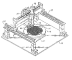
Referring now to the drawings, apparatus constructed in accordance with the present invention includes a precision rotary stage or wafer support 10 is rigidly mounted to a base plate 12 with the axis of rotation thereof normal to the surface of the base plate. A porous ceramic vacuum chuck 14 is mounted on top of the rotary stage 10. The semiconductor wafer 16 to be scribed is placed on the vacuum chuck 14.
A multi-stage gantry 20 consisting of three precision linear stages is mounted on the base plate 12 adjacent to the wafer support. The first linear stage of the gantry is comprised of a pair of first linear stage side segments 22 disposed at opposed sides of the wafer support. Each linear stage side segment includes a high precision bearing 24, a linear motor 26, and a high precision linear encoder 28. In the preferred embodiment of the invention, the precision bearing 24 may be an air bearing or an ultra high precision rail and block bearing using recirculating balls or rollers. The linear motor 26 may be a U-channel style of linear motor, a thrust tube style of linear motor, or a piezoelectic linear motor.
A second linear stage, the cross stage 30 of the gantry, is comprised of a high precision bearing 32, a linear motor 34, and a high precision linear encoder 36. In the preferred embodiment of the invention, the precision bearing 32 is an air bearing. The linear motor 34 may be U-channel style of linear motor, a thrust tube style of linear motor, or a piezoelectic linear motor.
A third precision linear stage 40 is mounted vertically on the bearing block 42 of the gantry cross stage bearing 32. The vertical stage 40 is comprised of a high precision bearing including shaft 44, a linear motor 46, and a high precision linear encoder 48. In the preferred embodiment of the invention, the precision bearing is an air bearing. The linear motor 46 may be a U-channel style of linear motor, a thrust tube style of linear motor, or a piezoelectric linear motor. The vertical stage is mounted differently than the other linear stages. The bearing block 50 of the vertical stage is rigidly mounted to the bearing block 42 of the cross stage while the vertical stage air bearing shaft 44 is allowed to move.
The force measurement structure 60 is mounted at the lower end of the vertical stage air bearing shaft 44 by a small, high precision rotary stage 54. Force measurement structure 60 is on the rotary stage. The scribe tool holder 52 at the end of the force measurement structure 60 provides a means to hold a diamond scribe tool 64 which is comprised of a diamond scribe tip 66 mounted on one end of a stainless steel shaft.
A high power microscope 70 is mounted on the cross stage bearing block 42 and a video camera 72 is mounted on the top of the microscope.
The invention incorporates a unique force measurement and control arrangement. With particular reference to FIGS. 7-11, parallel flexible strips or beams 74 are held at one end of thereof in a rigid mount 76 incorporated on the scribe tool holder. The flexible beams comprise part of the scribe tool holder and are located between the scribe tool and the rigid mount 76, allowing deflection of the tool holder. An encoder scale 78 is mounted on the rear side of the scribe tool holder 52. Located on the rigid mount 76, in a position to view the encoder scale, is a precision linear encoder 79. The rigid mount 76 is connected to the end of the vertical air bearing shaft 44 by way of the small, high precision rotary stage 54., The vertical air bearing shaft 44 is moved by the vertical stage linear motor 46.
FIG. 12 is a simplified drawing of the control system used in this invention. The mechanism described above is connected by appropriate cables to servo amplifiers 80 and a control computer or controller 82. Video signals from the video camera 72 on the microscope 70 are transmitted by appropriate cables to a video signal controller 84, the latter being connected to the control computer 82.
With regard to operation of the apparatus, rotary stage 10 is rotated, allowing circuits or devices on the wafer to be aligned relative to the lateral and distal/proximal motion of the first and second gantry stages. The rotary stage 10 also allows the wafer to be rotated 90 degrees in order to scribe the second direction on the wafer surface, During operation of the apparatus, the rotary stage 10 and wafer are fixed against movement as previously described.
The lateral motion of the diamond scribe tip relative to the surface of the wafer is effected by the cross stage 30 and the indexing of the diamond scribe from the distal edge of the wafer to the proximal edge of the wafer is effected by the gantry stages comprising stage side segments 22 (see FIG. 3).
The angle at which the diamond scribe tip addresses the wafer surface is effected by the small rotary stage 54. The vertical stage 40 of the gantry provides the means to raise and lower the diamond scribe tip relative to the wafer surface as well as to control the force that the diamond scribe tip applies to the wafer (see FIGS. 4, 7-10).
When the diamond scribe tip is pressed into the surface of the wafer, the flexible beams 74 will bend and the tool holder 52 will deflect in direct proportion to the force applied by the diamond scribe tip to the wafer surface (see FIG. 8). This deflection is measured by the encoder 79 reading the encoder scale 78 mounted on the tool holder 52. If the force is smaller than desired, the linear motor 46 of vertical stage 40 is used to move the vertical stage shaft 44 down, thus deflecting the flexible beams 74 by a greater amount and applying a larger force by the diamond scribe tip to the surface of the wafer.
The control system operates by determining the position of each stage in the apparatus by reading the output signal from its associated encoder. These signals are conducted through appropriate cabling to the servo amplifiers 80 where they are used to configure and control the electronic commutation of the motors. The encoder signals are then passed through appropriate cabling to the control computer 82. In the controller 82 the positions of the mechanism stages, as indicated by the associated encoder signals, are compared to the desired positions and command signals are generated that are sent to the appropriate servo amplifiers 80. The servo amplifiers 80 then send the appropriate motor control signals to the stages of the apparatus.
The encoder signal from the force sensor encoder is conducted by appropriate cabling directly to the control computer 82. The control computer 82 analyzes the signal from the force encoder and sends an appropriate servo amplifier command signal to the vertical stage servo amplifier, which in turn then sends the appropriate motor control signal to the vertical stage motor to control the force.
The output signal from the video camera 72 on the microscope 70 is conducted through appropriate cabling to a video signal controller 84. The video signal is then passed to the controller 82 where it is displayed on a computer monitor as well as being used by the computer to implement pattern recognition and machine vision software routines. In addition to the direct monitoring and mechanism control functions it performs, the control computer 82 also contains software routines to select different process conditions and to provide fully automatic sequencing of the motions of the stages of the apparatus to perform the desired scribing process.
Apparatus constructed in accordance with the teachings this invention has exhibited significantly improved performance over what is currently known in the art. The linear speed of the diamond scribe tip relative to the wafer is 5×-10×faster than existing wafer scribing apparatus resulting in a proportional increase in manufacturing efficiency of wafer scribing. Using linear encoders with a resolution of 0.1 micron, the apparatus has a precision of positioning control of a few tenths of microns compared to around 1.0 microns that is currently known in the art. This improved control of the positioning of the diamond scribe tip relative to the surface of the wafer results in more consistent positioning and directional control of the scribe line, which in turn results in a higher yield of successfully cleaved circuits or devices.
To achieve these results, the linear motors used on the gantry side stage segments are Thrusttube motors, model number T1106, manufactured by Copley Controls Corporation. The linear motor used on the gantry cross stage is a Thrusttube motor, model number T1108, manufactured by Copley Controls Corporation. The linear motor used on the vertical stage is a Thrusttube motor, model number T1106, manufactured by Copley Controls Corpoation. The bearings used on the end gantry stages are model number SHS15VUU-324LUP, manufactured by THK Company, Ltd. The encoders used on all of the linear stages and on the force sensor are model number RGH25U15J00A, manufactured by Renishaw Inc.
The flexible beams used in the force measurement portion of this invention may be made of any suitably flexible, resilient material, such as stainless steel, spring steel, titanium, beryllium cooper, etc. In our early investigations, the material chosen was 304 stainless steel. The number of beams used should be greater than 1 to prevent torsion twisting of the beam but can be any greater number. In our early investigations, we chose to use four beams as a good compromise between limiting torsion twisting and achieving reasonable flexure response. Using four beams made from 0.010 inch thick 304 stainless steel resulted in approximately 6 microns of motion measured by the encoder for each gram of force between the diamond scribe tip and the wafer surface. Using a 0.1 micron resolution encoder resulted in 60 encoder counts per gram of force between the diamond scribe tip and the wafer surface. This results in the ability to control the force between the diamond scribe tip and the wafer surface to within a few tenths of a gram. In addition, since the linear encoder is a digital device, it is more tolerant of electrical noise from the motor drive system than an analog device such as a load cell. This improved control of the force between the diamond scribe tip and the surface of the wafer results in more consistent control of scribe line depth and of the stress imparted to the material near the scribe line. This, in turn, results in a higher yield of successfully cleaved circuits or devices.

Claims (25)

What is claimed is:
1. Apparatus for scribing semiconductor wafers comprising, in combination:
a wafer support for rigidly supporting a wafer and maintaining said wafer against movement;
a scribe tool;
a scribe tool holder holding said scribe tool;
support structure supporting said scribe tool holder, said support structure operable to selectively bring said scribe tool into engagement with said wafer and to move said scribe tool relative to said wafer while in engagement therewith and while said wafer is rigidly supported by and maintained against movement by said wafer support to form a scribe line in said wafer, said scribe tool holder including at least one flexible scribe tool holder element located adjacent to said scribe tool and bendable responsive to pressure being exerted on a wafer fixedly held on said wafer support by said scribe tool.
2. The apparatus according to claim 1 wherein said support structure is a multi-stage support structure including a first linear stage comprising a pair of first linear stage side segments disposed at opposed sides of said wafer support for moving said scribe tool holder and scribe tool in a first predetermined direction, a second linear stage extending between and movable relative to said first linear side segments for moving said scribe tool holder and scribe tool in a second predetermined direction, and a third linear stage depending from said second linear stage for moving said scribe tool holder and said scribe tool selectively toward or away from said wafer support.
3. The apparatus according to claim 2 wherein at least one of said linear stages includes a bearing, a linear motor movable relative to said bearing and a linear encoder operatively associated with said linear motor for providing linear encoder output signals indicating the position of said linear motor relative to said bearing to a controller employed to control operation of the multi-stage support structure.
4. The apparatus according to claim 3 wherein said bearing is a rigid elongated member.
5. The apparatus according to claim 4 wherein said bearing is an air bearing.
6. The apparatus according to claim 2 wherein said third linear stage includes a linear motor and a shaft operatively associated with said linear motor and vertically movable with respect thereto, said scribe tool holder being connected to and movable with said shaft in a vertical direction.
7. The apparatus according to claim 6 wherein said shaft is an air bearing.
8. The apparatus according to claim 6 wherein said third linear stage further includes a linear encoder operatively associated with said linear motor and said shaft for providing linear encoder output signals indicating the position of said shaft relative to said linear motor to a controller employed to control operation of the multi-stage support structure.
9. The apparatus according to claim 2 wherein said first linear stage and said second linear stage each include a bearing, a linear motor movable along said bearing and a linear encoder operatively associated with said linear motor and said bearing for providing linear encoder output signals indicating the position of said linear motor relative to said bearing to a controller employed to control operation of said multi-stage support structure, said first and second predetermined directions being orthogonal to one another.
10. The apparatus according to claim 1 wherein said scribe tool holder is selectively rotatably adjustable to adjust the angle at which the scribe tool addresses a surface of a wafer rigidly supported by said wafer support.
11. The apparatus according to claim 1 additionally comprising a sensor operatively associated with said scribe tool holder to sense bending of said at least one flexible scribe holder element.
12. The apparatus according to claim 11 wherein said sensor comprises an encoder for measuring deflection of said scribe holder.
13. The apparatus according to claim 12 wherein said scribe holder includes an encoder scale readable by said encoder.
14. The apparatus according to claim 12 wherein said support structure is a multi-stage support structure including a linear stage for moving said scribe tool holder and said scribe tool selectively toward or away from said wafer support, said encoder comprising part of said linear stage and providing encoder output signals directly proportional to deflection of said scribe tool holder.
15. The apparatus according to claim 14 wherein said linear gantry stage additionally includes a linear motor and a shaft operatively associated with said linear motor and movable with respect thereto, said scribe tool holder being connected to said shaft and movable therewith, movement of said shaft and said scribe tool holder being responsive to output signals from said encoder.
16. The apparatus according to claim 14 wherein said encoder is a digital encoder and wherein said encoder output signals are digital signals.
17. The apparatus according to claim 1 wherein said scribe tool holder includes a plurality of flexible scribe tool holder elements.
18. The apparatus according to claim 17 wherein said flexible scribe tool holder elements comprise substantially parallel, flexible beams cooperable to resist torsional twisting of said scribe tool holder.
19. A method for scribing semiconductor wafers, said method comprising the steps of:
rigidly supporting a wafer on a wafer support;
maintaining said wafer support and wafer against movement;
supporting a scribe tool holder holding a scribe tool from support structure disposed adjacent to said wafer support;
employing said support structure to selectively move said scribe tool holder and selectively bring said scribe tool into engagement with said wafer; and
while said scribe tool is in engagement with said wafer and while said wafer is rigidly supported on and maintained against movement by said wafer support, utilizing said support structure to move said scribe tool holder and scribe tool relative to said wafer to form a scribe line in said wafer, said scribe tool holder including at least one flexible scribe tool holder element adjacent to said scribe tool, said method including the step of bending said at least one flexible scribe tool holder element responsive to pressure being exerted on said wafer by said scribe tool.
20. The method according to claim 19 wherein said support structure includes a linear stage including a linear motor, a bearing supporting said linear motor and a linear encoder, said method further comprising the steps of:
utilizing the linear encoder to sense the position of said linear motor on said bearing;
providing output signals from said linear encoder to a controller indicating the position of said linear motor relative to said bearing; and
utilizing said controller to selectively reposition said linear motor relative to said bearing.
21. The method according to claim 19 including the step of adjusting the angle at which said scribe tool addresses a surface of the wafer prior to the step of bringing the scribe tool into engagement with said wafer.
22. The method according to claim 19 including the additional step of employing a sensor to sense bending of said at least one flexible scribe tool holder element.
23. The method according to claim 22 wherein said sensor comprises an encoder, said method including utilizing said encoder to measure deflection of said scribe tool holder.
24. The method according to claim 23 wherein said support structure is a multi-stage support member including a linear stage, said method including employing said linear stage to move said scribe tool holder and said scribe tool selectively toward or away from said wafer support and wafer, said method further including utilizing said encoder to generate encoder output signals sent to a controller directly proportional to deflection of said scribe holder when said scribe engages the wafer, and responsive to receipt of said encoder output signals by said controller, utilizing said controller to control operation of said linear stage to selectively vary the pressure exerted by said scribe tool on said wafer.
25. The method according to claim 24 wherein said encoder is a digital encoder and wherein said output signals are digital signals.
US10/462,398 2003-06-16 2003-06-16 Semiconductor wafer scribing system Expired - Fee Related US6826840B1 (en)

Priority Applications (1)

Application Number Priority Date Filing Date Title
US10/462,398 US6826840B1 (en) 2003-06-16 2003-06-16 Semiconductor wafer scribing system

Applications Claiming Priority (1)

Application Number Priority Date Filing Date Title
US10/462,398 US6826840B1 (en) 2003-06-16 2003-06-16 Semiconductor wafer scribing system

Publications (1)

Publication Number Publication Date
US6826840B1 true US6826840B1 (en) 2004-12-07

Family

ID=33476647

Family Applications (1)

Application Number Title Priority Date Filing Date
US10/462,398 Expired - Fee Related US6826840B1 (en) 2003-06-16 2003-06-16 Semiconductor wafer scribing system

Country Status (1)

Country Link
US (1) US6826840B1 (en)

Cited By (23)

* Cited by examiner, † Cited by third party
Publication number Priority date Publication date Assignee Title
US20030048448A1 (en) * 2001-03-19 2003-03-13 Fleming Timothy J. Automated apparatus for testing optical filters
US20030048455A1 (en) * 2001-03-19 2003-03-13 Fleming Timothy J. Goniometer
US20030059100A1 (en) * 2001-03-19 2003-03-27 Fleming Timothy J. Method and apparatus for calibrating a vision system to a parts handling device
US20050005466A1 (en) * 2003-07-07 2005-01-13 Samsung Electronics Co., Ltd. Apparatus for measuring horizontal level of a wafer chuck
US20050174139A1 (en) * 2003-10-14 2005-08-11 Mahendran Chidambaram Apparatus for high speed probing of flat panel displays
US20050181527A1 (en) * 2002-07-22 2005-08-18 Sumitomo Electric Industries, Ltd., A Osaka, Japan Corporation Method for forming scribed groove and scribing apparatus
US20060179670A1 (en) * 2005-02-15 2006-08-17 Columbia Marking Tools Apparatus and method for controlling a programmable marking scribe
US7165331B1 (en) * 2005-05-24 2007-01-23 Micro Processing Technology, Inc. Apparatus and method for scribing a semiconductor wafer while controlling scribing forces
US20070186426A1 (en) * 2006-02-16 2007-08-16 Precise Automation. Llc Robotic system with traction drive
NL2000501C2 (en) * 2007-02-22 2008-08-25 Consulo Device and method for diagnosing a disorder.
CN100435314C (en) * 2005-07-12 2008-11-19 Lkt自动化配备私人有限公司 Adjustable tool holder
US20110023593A1 (en) * 2009-08-03 2011-02-03 HONG FU JIN PRECISION INDUSTRY (ShenZhen CO., LTD. Coating rigidity testing device
US20110168039A1 (en) * 2010-01-13 2011-07-14 Roland Dg Corporation Stamping machine
US8220685B1 (en) * 2005-09-08 2012-07-17 Micro Processing Technology, Inc. System for breaking a semiconductor wafer or other workpiece along a scribe line
US20130008042A1 (en) * 2010-03-10 2013-01-10 Kuroda Precision Industries Ltd. Control Device for a Parallel Slider Device, Control Method Therefor and Measuring Device Using Same
US8375594B1 (en) * 2010-06-09 2013-02-19 Bruker Nano Inc. Pneumatic counterbalance for optical head gantry
US8450188B1 (en) 2011-08-02 2013-05-28 Micro Processing Technology, Inc. Method of removing back metal from an etched semiconductor scribe street
US20160379849A1 (en) * 2015-06-23 2016-12-29 LatticeGear, LLC Device and method for scribing a bottom-side of a substrate while viewing the top side
US20170227343A1 (en) * 2014-04-04 2017-08-10 Hexagon Metrology, Inc. Coordinate measuring machine with carbon fiber air bearings
CN109176928A (en) * 2018-09-14 2019-01-11 苏州迈为科技股份有限公司 A kind of cell piece dicing device and dicing method
USD863389S1 (en) * 2017-11-28 2019-10-15 Red Technology Co., Ltd. Portable dot peen marking machine
CN112201600A (en) * 2020-10-14 2021-01-08 北京中科镭特电子有限公司 Wafer splitting and expanding device and wafer splitting and expanding method
CN112201600B (en) * 2020-10-14 2024-03-08 北京中科镭特电子有限公司 Wafer splitting and expanding device and wafer splitting and expanding method

Citations (7)

* Cited by examiner, † Cited by third party
Publication number Priority date Publication date Assignee Title
US3094785A (en) 1960-12-20 1963-06-25 Kulicke & Soffa Mfg Co Automatic semi-conductor wafer scriber
US3680213A (en) * 1969-02-03 1972-08-01 Karl O Reichert Method of grooving semiconductor wafer for the dividing thereof
US4502225A (en) 1983-05-06 1985-03-05 Rca Corporation Mechanical scriber for semiconductor devices
US4697348A (en) * 1984-09-06 1987-10-06 United Innovations Division Of United Engineers, Inc. Positioning systems
US4825555A (en) * 1986-10-31 1989-05-02 Dainippon Screen Mfg. Co., Ltd. Apparatus for automatic forming on a film material of both a mask film pattern and a positioning hole
US5820006A (en) 1994-01-18 1998-10-13 Dynatex International, Inc. Apparatus for scribing and/or breaking semiconductor wafers
US20030177650A1 (en) * 2002-03-19 2003-09-25 Beldex Corporation Scribe device

Patent Citations (7)

* Cited by examiner, † Cited by third party
Publication number Priority date Publication date Assignee Title
US3094785A (en) 1960-12-20 1963-06-25 Kulicke & Soffa Mfg Co Automatic semi-conductor wafer scriber
US3680213A (en) * 1969-02-03 1972-08-01 Karl O Reichert Method of grooving semiconductor wafer for the dividing thereof
US4502225A (en) 1983-05-06 1985-03-05 Rca Corporation Mechanical scriber for semiconductor devices
US4697348A (en) * 1984-09-06 1987-10-06 United Innovations Division Of United Engineers, Inc. Positioning systems
US4825555A (en) * 1986-10-31 1989-05-02 Dainippon Screen Mfg. Co., Ltd. Apparatus for automatic forming on a film material of both a mask film pattern and a positioning hole
US5820006A (en) 1994-01-18 1998-10-13 Dynatex International, Inc. Apparatus for scribing and/or breaking semiconductor wafers
US20030177650A1 (en) * 2002-03-19 2003-09-25 Beldex Corporation Scribe device

Cited By (35)

* Cited by examiner, † Cited by third party
Publication number Priority date Publication date Assignee Title
US20030048455A1 (en) * 2001-03-19 2003-03-13 Fleming Timothy J. Goniometer
US20030059100A1 (en) * 2001-03-19 2003-03-27 Fleming Timothy J. Method and apparatus for calibrating a vision system to a parts handling device
US6983547B2 (en) 2001-03-19 2006-01-10 Veeco Instruments Inc. Goniometer
US7065892B2 (en) * 2001-03-19 2006-06-27 Veeco Instruments Inc. Method and apparatus for calibrating a vision system to a parts handling device
US20030048448A1 (en) * 2001-03-19 2003-03-13 Fleming Timothy J. Automated apparatus for testing optical filters
US20050181527A1 (en) * 2002-07-22 2005-08-18 Sumitomo Electric Industries, Ltd., A Osaka, Japan Corporation Method for forming scribed groove and scribing apparatus
US7131209B2 (en) * 2003-07-07 2006-11-07 Samsung Electronics Co., Ltd. Apparatus for measuring horizontal level of a wafer chuck
US20050005466A1 (en) * 2003-07-07 2005-01-13 Samsung Electronics Co., Ltd. Apparatus for measuring horizontal level of a wafer chuck
US20050174139A1 (en) * 2003-10-14 2005-08-11 Mahendran Chidambaram Apparatus for high speed probing of flat panel displays
US20060179670A1 (en) * 2005-02-15 2006-08-17 Columbia Marking Tools Apparatus and method for controlling a programmable marking scribe
WO2006088991A2 (en) * 2005-02-15 2006-08-24 Columbia Marking Tools Apparatus and method for controlling a programmable marking scribe
WO2006088991A3 (en) * 2005-02-15 2007-01-11 Columbia Marking Tools Apparatus and method for controlling a programmable marking scribe
US7191529B2 (en) * 2005-02-15 2007-03-20 Columbia Marking Tools Apparatus and method for controlling a programmable marking scribe
US7165331B1 (en) * 2005-05-24 2007-01-23 Micro Processing Technology, Inc. Apparatus and method for scribing a semiconductor wafer while controlling scribing forces
CN100435314C (en) * 2005-07-12 2008-11-19 Lkt自动化配备私人有限公司 Adjustable tool holder
US8220685B1 (en) * 2005-09-08 2012-07-17 Micro Processing Technology, Inc. System for breaking a semiconductor wafer or other workpiece along a scribe line
US20070186426A1 (en) * 2006-02-16 2007-08-16 Precise Automation. Llc Robotic system with traction drive
US7343684B2 (en) * 2006-02-16 2008-03-18 Brian Carlisle Robotic system with traction drive
NL2000501C2 (en) * 2007-02-22 2008-08-25 Consulo Device and method for diagnosing a disorder.
US8215163B2 (en) * 2009-08-03 2012-07-10 Hong Fu Jin Precision Industry (Shenzhen) Co., Ltd. Coating rigidity testing device
US20110023593A1 (en) * 2009-08-03 2011-02-03 HONG FU JIN PRECISION INDUSTRY (ShenZhen CO., LTD. Coating rigidity testing device
US20110168039A1 (en) * 2010-01-13 2011-07-14 Roland Dg Corporation Stamping machine
US8539683B2 (en) * 2010-01-13 2013-09-24 Roland Dg Corporation Stamping machine
US20130008042A1 (en) * 2010-03-10 2013-01-10 Kuroda Precision Industries Ltd. Control Device for a Parallel Slider Device, Control Method Therefor and Measuring Device Using Same
US8819952B2 (en) * 2010-03-10 2014-09-02 Kuroda Precision Industries Ltd. Control device for a parallel slider device, control method and measuring device using same
US8375594B1 (en) * 2010-06-09 2013-02-19 Bruker Nano Inc. Pneumatic counterbalance for optical head gantry
US8450188B1 (en) 2011-08-02 2013-05-28 Micro Processing Technology, Inc. Method of removing back metal from an etched semiconductor scribe street
US10323920B2 (en) * 2014-04-04 2019-06-18 Hexagon Metrology, Inc. Coordinate measuring machine with carbon fiber air bearings
US20170227343A1 (en) * 2014-04-04 2017-08-10 Hexagon Metrology, Inc. Coordinate measuring machine with carbon fiber air bearings
US10068782B2 (en) * 2015-06-23 2018-09-04 LatticeGear, LLC Device and method for scribing a bottom-side of a substrate while viewing the top side
US20160379849A1 (en) * 2015-06-23 2016-12-29 LatticeGear, LLC Device and method for scribing a bottom-side of a substrate while viewing the top side
USD863389S1 (en) * 2017-11-28 2019-10-15 Red Technology Co., Ltd. Portable dot peen marking machine
CN109176928A (en) * 2018-09-14 2019-01-11 苏州迈为科技股份有限公司 A kind of cell piece dicing device and dicing method
CN112201600A (en) * 2020-10-14 2021-01-08 北京中科镭特电子有限公司 Wafer splitting and expanding device and wafer splitting and expanding method
CN112201600B (en) * 2020-10-14 2024-03-08 北京中科镭特电子有限公司 Wafer splitting and expanding device and wafer splitting and expanding method

Similar Documents

Publication Publication Date Title
US6826840B1 (en) Semiconductor wafer scribing system
JP2896746B2 (en) Work holder for rotary grinding machine for grinding semiconductor wafers and method for positioning the work holder
KR100269964B1 (en) Work piece position decision method and its apparatus
KR102080447B1 (en) Kinematic holding system for a placement head of a placement apparatus
JPS6336888B2 (en)
US7165331B1 (en) Apparatus and method for scribing a semiconductor wafer while controlling scribing forces
CN101146657B (en) Scribe device
EP2189235A1 (en) Bond head for heavy wire bonder with first module and second lockable/unlockabe module
KR100663939B1 (en) Long range stage with full stroke nano resolution for high vacuum
JP2007054922A (en) Grinding apparatus and grinding method for plate-like material to be ground
JPH106199A (en) Curved surface polishing method and curved surface polishing device
US6758721B2 (en) Apparatus and method for lapping magnetic heads
WO2001096068A1 (en) Device and method for measuring amount of grinding in magnetic head producing process
WO2010020778A1 (en) High speed shear test device and method
JPH11198018A (en) Endless wire saw attached with stationary abrasive grain
CN103501943A (en) Stabilizing device for a cutting disk
CN108557756B (en) A kind of micromachined knife rest with force servo function
KR101976997B1 (en) Apparatus and Method for forming a probe pin
US20040094010A1 (en) Cutting device for breaking fragile materials such as semiconductor wafers or the like
WO2022259641A1 (en) Deburring device and deburring unit
JPH1074712A (en) Wafer breaking device
CN220388129U (en) Mounting device for a workpiece and machining system
JP3544159B2 (en) Peeling / cleaning equipment
JP4118022B2 (en) Scribing method and scribing apparatus
JP2001110754A (en) Cutting device

Legal Events

Date Code Title Description
AS Assignment

Owner name: MICRO PROCESSING TECHNOLOGY INC., CALIFORNIA

Free format text: ASSIGNMENT OF ASSIGNORS INTEREST;ASSIGNORS:LINDSEY, PAUL C.;ATKINSON, JEFFREY D.;REEL/FRAME:014185/0937

Effective date: 20030611

FEPP Fee payment procedure

Free format text: PAYOR NUMBER ASSIGNED (ORIGINAL EVENT CODE: ASPN); ENTITY STATUS OF PATENT OWNER: SMALL ENTITY

FPAY Fee payment

Year of fee payment: 4

FPAY Fee payment

Year of fee payment: 8

REMI Maintenance fee reminder mailed
LAPS Lapse for failure to pay maintenance fees
STCH Information on status: patent discontinuation

Free format text: PATENT EXPIRED DUE TO NONPAYMENT OF MAINTENANCE FEES UNDER 37 CFR 1.362

FP Lapsed due to failure to pay maintenance fee

Effective date: 20161207