US6806509B2 - Light-emitting semiconductor potting composition and light-emitting semiconductor device - Google Patents
Light-emitting semiconductor potting composition and light-emitting semiconductor device Download PDFInfo
- Publication number
- US6806509B2 US6806509B2 US10/797,139 US79713904A US6806509B2 US 6806509 B2 US6806509 B2 US 6806509B2 US 79713904 A US79713904 A US 79713904A US 6806509 B2 US6806509 B2 US 6806509B2
- Authority
- US
- United States
- Prior art keywords
- light
- emitting semiconductor
- composition
- cured
- semiconductor device
- Prior art date
- Legal status (The legal status is an assumption and is not a legal conclusion. Google has not performed a legal analysis and makes no representation as to the accuracy of the status listed.)
- Expired - Lifetime
Links
- GLVBGZSAQSKIRJ-UHFFFAOYSA-N C=C[Si](C)(C)O[Si](C)(C)O[Si](C)(C)C=C.[H][Si](C)(C)O[Si]([H])(C)O[Si](C)(C)O[Si]([H])(C)C Chemical compound C=C[Si](C)(C)O[Si](C)(C)O[Si](C)(C)C=C.[H][Si](C)(C)O[Si]([H])(C)O[Si](C)(C)O[Si]([H])(C)C GLVBGZSAQSKIRJ-UHFFFAOYSA-N 0.000 description 2
- UHHGHJCFXFPHQG-UHFFFAOYSA-N C=C[Si](C)(C)O[Si](C)(C)O[Si](O[Si](C)(C)C=C)(C1=CC=CC=C1)C1=CC=CC=C1.[H][Si](C)(C)O[Si]([H])(C)O[Si](C)(C)O[Si]([H])(C)C Chemical compound C=C[Si](C)(C)O[Si](C)(C)O[Si](O[Si](C)(C)C=C)(C1=CC=CC=C1)C1=CC=CC=C1.[H][Si](C)(C)O[Si]([H])(C)O[Si](C)(C)O[Si]([H])(C)C UHHGHJCFXFPHQG-UHFFFAOYSA-N 0.000 description 2
- MLOZMNYRRLJJSY-UHFFFAOYSA-N C=C[Si](C)(C)O[Si](C)(C)OCC[Si](O[Si](C)(C)O[Si](C)(C)C=C)(O[Si](O[Si](C)(C)C=C)(C1=CC=CC=C1)C1=CC=CC=C1)C1=CC=CC=C1.C=C[Si](C)(C)O[Si](C)(C)O[Si](O[Si](C)(C)C=C)(C1=CC=CC=C1)C1=CC=CC=C1.C=C[Si](C)(C)O[Si](C)(C)O[Si](O[Si](C)(C)C=C)(C1=CC=CC=C1)C1=CC=CC=C1.C=C[Si](C)(C)O[Si](C)(C)O[Si](O[Si](C)(O[Si](C)(C)C=C)C1=CC=CC=C1)(C1=CC=CC=C1)C1=CC=CC=C1 Chemical compound C=C[Si](C)(C)O[Si](C)(C)OCC[Si](O[Si](C)(C)O[Si](C)(C)C=C)(O[Si](O[Si](C)(C)C=C)(C1=CC=CC=C1)C1=CC=CC=C1)C1=CC=CC=C1.C=C[Si](C)(C)O[Si](C)(C)O[Si](O[Si](C)(C)C=C)(C1=CC=CC=C1)C1=CC=CC=C1.C=C[Si](C)(C)O[Si](C)(C)O[Si](O[Si](C)(C)C=C)(C1=CC=CC=C1)C1=CC=CC=C1.C=C[Si](C)(C)O[Si](C)(C)O[Si](O[Si](C)(O[Si](C)(C)C=C)C1=CC=CC=C1)(C1=CC=CC=C1)C1=CC=CC=C1 MLOZMNYRRLJJSY-UHFFFAOYSA-N 0.000 description 1
- JHEAVSYFTRWNGT-UHFFFAOYSA-N C=C[Si](C)(C)O[Si](C)(C)O[Si](OC)(OC)OC.C=C[Si](C)(O[Si](C)(C)O[Si](CCCOC(C)C1CO1)(OC)OC)O[Si](CCCOCC1CO1)(OC)OC.[H][Si](C)(C)O[Si](C)(C)O[Si](OC)(OC)OC.[H][Si](C)(O[Si](C)(C)C)O[SiH]1(C)(O[Si](C)(C)O[SiH]2(C)(O[Si](C)(C)C)CC2[Si](OC)(OC)OC)CCC1OCC1CO1 Chemical compound C=C[Si](C)(C)O[Si](C)(C)O[Si](OC)(OC)OC.C=C[Si](C)(O[Si](C)(C)O[Si](CCCOC(C)C1CO1)(OC)OC)O[Si](CCCOCC1CO1)(OC)OC.[H][Si](C)(C)O[Si](C)(C)O[Si](OC)(OC)OC.[H][Si](C)(O[Si](C)(C)C)O[SiH]1(C)(O[Si](C)(C)O[SiH]2(C)(O[Si](C)(C)C)CC2[Si](OC)(OC)OC)CCC1OCC1CO1 JHEAVSYFTRWNGT-UHFFFAOYSA-N 0.000 description 1
- FWAFYWSMKJKQJI-UHFFFAOYSA-N C=C[Si](C)(C)O[Si](C)(C)O[Si](O[Si](C)(C)C=C)(C1=CC=CC=C1)C1=CC=CC=C1 Chemical compound C=C[Si](C)(C)O[Si](C)(C)O[Si](O[Si](C)(C)C=C)(C1=CC=CC=C1)C1=CC=CC=C1 FWAFYWSMKJKQJI-UHFFFAOYSA-N 0.000 description 1
- CPSDVVMHJBTCSS-UHFFFAOYSA-N C=C[Si](C)(C)O[Si](C)(C)O[Si](O[Si](C)(C)C=C)(C1=CC=CC=C1)C1=CC=CC=C1.[H][Si](C)(C)O[Si](C)(C)O[Si](OC)(OC)OC.[H][Si](C)(C)O[Si](O[Si]([H])(C)C)(O[Si]([H])(C)C)C1=CC=CC=C1 Chemical compound C=C[Si](C)(C)O[Si](C)(C)O[Si](O[Si](C)(C)C=C)(C1=CC=CC=C1)C1=CC=CC=C1.[H][Si](C)(C)O[Si](C)(C)O[Si](OC)(OC)OC.[H][Si](C)(C)O[Si](O[Si]([H])(C)C)(O[Si]([H])(C)C)C1=CC=CC=C1 CPSDVVMHJBTCSS-UHFFFAOYSA-N 0.000 description 1
- ZRSINDFGOHFXAY-UHFFFAOYSA-N CO[Si](C)(C)C.CO[Si](C)(C)C1=CC=CC=C1.CO[Si](C)(C1=CC=CC=C1)C1=CC=CC=C1 Chemical compound CO[Si](C)(C)C.CO[Si](C)(C)C1=CC=CC=C1.CO[Si](C)(C1=CC=CC=C1)C1=CC=CC=C1 ZRSINDFGOHFXAY-UHFFFAOYSA-N 0.000 description 1
- QUHITNXQBKGHFN-UHFFFAOYSA-N [H][Si](C)(C)O[Si]([H])(C)O[Si](C)(C)O[Si]([H])(C)C.[H][Si]1(C)CCCCO[Si](C)(CCCOCC2CO2)O[Si](C)(CC[Si](OC)(OC)OC)O1 Chemical compound [H][Si](C)(C)O[Si]([H])(C)O[Si](C)(C)O[Si]([H])(C)C.[H][Si]1(C)CCCCO[Si](C)(CCCOCC2CO2)O[Si](C)(CC[Si](OC)(OC)OC)O1 QUHITNXQBKGHFN-UHFFFAOYSA-N 0.000 description 1
- ZISQZTPWLOCXDO-UHFFFAOYSA-N [H][Si]1(C)CCCCO[SiH]2(C)(CCC2OCC2CO2)O[Si](C)(CC[Si](OC)(OC)OC)O1.[H][Si]1(C)CCCCO[Si](C)(CC[Si](OC)(OC)OC)O1.[H][Si]1(C)CCCCO[Si](C)(CC[Si](OC)(OC)OC)O1 Chemical compound [H][Si]1(C)CCCCO[SiH]2(C)(CCC2OCC2CO2)O[Si](C)(CC[Si](OC)(OC)OC)O1.[H][Si]1(C)CCCCO[Si](C)(CC[Si](OC)(OC)OC)O1.[H][Si]1(C)CCCCO[Si](C)(CC[Si](OC)(OC)OC)O1 ZISQZTPWLOCXDO-UHFFFAOYSA-N 0.000 description 1
Images


Classifications
-
- H—ELECTRICITY
- H10—SEMICONDUCTOR DEVICES; ELECTRIC SOLID-STATE DEVICES NOT OTHERWISE PROVIDED FOR
- H10H—INORGANIC LIGHT-EMITTING SEMICONDUCTOR DEVICES HAVING POTENTIAL BARRIERS
- H10H20/00—Individual inorganic light-emitting semiconductor devices having potential barriers, e.g. light-emitting diodes [LED]
- H10H20/80—Constructional details
- H10H20/85—Packages
- H10H20/852—Encapsulations
- H10H20/854—Encapsulations characterised by their material, e.g. epoxy or silicone resins
-
- C—CHEMISTRY; METALLURGY
- C08—ORGANIC MACROMOLECULAR COMPOUNDS; THEIR PREPARATION OR CHEMICAL WORKING-UP; COMPOSITIONS BASED THEREON
- C08L—COMPOSITIONS OF MACROMOLECULAR COMPOUNDS
- C08L83/00—Compositions of macromolecular compounds obtained by reactions forming in the main chain of the macromolecule a linkage containing silicon with or without sulfur, nitrogen, oxygen or carbon only; Compositions of derivatives of such polymers
- C08L83/04—Polysiloxanes
-
- C—CHEMISTRY; METALLURGY
- C08—ORGANIC MACROMOLECULAR COMPOUNDS; THEIR PREPARATION OR CHEMICAL WORKING-UP; COMPOSITIONS BASED THEREON
- C08G—MACROMOLECULAR COMPOUNDS OBTAINED OTHERWISE THAN BY REACTIONS ONLY INVOLVING UNSATURATED CARBON-TO-CARBON BONDS
- C08G77/00—Macromolecular compounds obtained by reactions forming a linkage containing silicon with or without sulfur, nitrogen, oxygen or carbon in the main chain of the macromolecule
- C08G77/04—Polysiloxanes
- C08G77/12—Polysiloxanes containing silicon bound to hydrogen
-
- C—CHEMISTRY; METALLURGY
- C08—ORGANIC MACROMOLECULAR COMPOUNDS; THEIR PREPARATION OR CHEMICAL WORKING-UP; COMPOSITIONS BASED THEREON
- C08G—MACROMOLECULAR COMPOUNDS OBTAINED OTHERWISE THAN BY REACTIONS ONLY INVOLVING UNSATURATED CARBON-TO-CARBON BONDS
- C08G77/00—Macromolecular compounds obtained by reactions forming a linkage containing silicon with or without sulfur, nitrogen, oxygen or carbon in the main chain of the macromolecule
- C08G77/04—Polysiloxanes
- C08G77/14—Polysiloxanes containing silicon bound to oxygen-containing groups
- C08G77/18—Polysiloxanes containing silicon bound to oxygen-containing groups to alkoxy or aryloxy groups
-
- C—CHEMISTRY; METALLURGY
- C08—ORGANIC MACROMOLECULAR COMPOUNDS; THEIR PREPARATION OR CHEMICAL WORKING-UP; COMPOSITIONS BASED THEREON
- C08G—MACROMOLECULAR COMPOUNDS OBTAINED OTHERWISE THAN BY REACTIONS ONLY INVOLVING UNSATURATED CARBON-TO-CARBON BONDS
- C08G77/00—Macromolecular compounds obtained by reactions forming a linkage containing silicon with or without sulfur, nitrogen, oxygen or carbon in the main chain of the macromolecule
- C08G77/04—Polysiloxanes
- C08G77/20—Polysiloxanes containing silicon bound to unsaturated aliphatic groups
-
- C—CHEMISTRY; METALLURGY
- C08—ORGANIC MACROMOLECULAR COMPOUNDS; THEIR PREPARATION OR CHEMICAL WORKING-UP; COMPOSITIONS BASED THEREON
- C08G—MACROMOLECULAR COMPOUNDS OBTAINED OTHERWISE THAN BY REACTIONS ONLY INVOLVING UNSATURATED CARBON-TO-CARBON BONDS
- C08G77/00—Macromolecular compounds obtained by reactions forming a linkage containing silicon with or without sulfur, nitrogen, oxygen or carbon in the main chain of the macromolecule
- C08G77/70—Siloxanes defined by use of the MDTQ nomenclature
-
- C—CHEMISTRY; METALLURGY
- C08—ORGANIC MACROMOLECULAR COMPOUNDS; THEIR PREPARATION OR CHEMICAL WORKING-UP; COMPOSITIONS BASED THEREON
- C08K—Use of inorganic or non-macromolecular organic substances as compounding ingredients
- C08K5/00—Use of organic ingredients
- C08K5/54—Silicon-containing compounds
-
- H—ELECTRICITY
- H10—SEMICONDUCTOR DEVICES; ELECTRIC SOLID-STATE DEVICES NOT OTHERWISE PROVIDED FOR
- H10W—GENERIC PACKAGES, INTERCONNECTIONS, CONNECTORS OR OTHER CONSTRUCTIONAL DETAILS OF DEVICES COVERED BY CLASS H10
- H10W72/00—Interconnections or connectors in packages
- H10W72/50—Bond wires
- H10W72/551—Materials of bond wires
- H10W72/552—Materials of bond wires comprising metals or metalloids, e.g. silver
- H10W72/5522—Materials of bond wires comprising metals or metalloids, e.g. silver comprising gold [Au]
-
- H—ELECTRICITY
- H10—SEMICONDUCTOR DEVICES; ELECTRIC SOLID-STATE DEVICES NOT OTHERWISE PROVIDED FOR
- H10W—GENERIC PACKAGES, INTERCONNECTIONS, CONNECTORS OR OTHER CONSTRUCTIONAL DETAILS OF DEVICES COVERED BY CLASS H10
- H10W72/00—Interconnections or connectors in packages
- H10W72/851—Dispositions of multiple connectors or interconnections
- H10W72/874—On different surfaces
- H10W72/884—Die-attach connectors and bond wires
-
- H—ELECTRICITY
- H10—SEMICONDUCTOR DEVICES; ELECTRIC SOLID-STATE DEVICES NOT OTHERWISE PROVIDED FOR
- H10W—GENERIC PACKAGES, INTERCONNECTIONS, CONNECTORS OR OTHER CONSTRUCTIONAL DETAILS OF DEVICES COVERED BY CLASS H10
- H10W90/00—Package configurations
- H10W90/701—Package configurations characterised by the relative positions of pads or connectors relative to package parts
- H10W90/731—Package configurations characterised by the relative positions of pads or connectors relative to package parts of die-attach connectors
- H10W90/736—Package configurations characterised by the relative positions of pads or connectors relative to package parts of die-attach connectors between a chip and a stacked lead frame, conducting package substrate or heat sink
-
- H—ELECTRICITY
- H10—SEMICONDUCTOR DEVICES; ELECTRIC SOLID-STATE DEVICES NOT OTHERWISE PROVIDED FOR
- H10W—GENERIC PACKAGES, INTERCONNECTIONS, CONNECTORS OR OTHER CONSTRUCTIONAL DETAILS OF DEVICES COVERED BY CLASS H10
- H10W90/00—Package configurations
- H10W90/701—Package configurations characterised by the relative positions of pads or connectors relative to package parts
- H10W90/751—Package configurations characterised by the relative positions of pads or connectors relative to package parts of bond wires
- H10W90/756—Package configurations characterised by the relative positions of pads or connectors relative to package parts of bond wires between a chip and a stacked lead frame, conducting package substrate or heat sink
Definitions
- This invention relates to a potting composition used for the embedment and protection of light-emitting semiconductor members and a light-emitting semiconductor device comprising a light-emitting semiconductor member embedded in the potting composition.
- LED light-emitting diodes
- Traditional light-emitting semiconductor devices such as light-emitting diodes (LED) are lamp-type light-emitting semiconductor devices in which a light-emitting semiconductor member is disposed on a lead electrode and encapsulated with a transparent resin to a cannonball shape as shown in FIG. 3 . They are recently replaced by the “surface mount” type as a result of simplification of the mounting technology.
- surface mounting light-emitting semiconductor devices as shown in FIGS. 1 and 2 become the mainstream.
- the device includes a housing 1 of glass fiber-reinforced epoxy resin, a light-emitting semiconductor member 2 , lead electrodes 3 and 4 , a die-bonding material 5 , gold wires 6 , and an encapsulant or potting composition 7 .
- compositions are used for the embedment of light-emitting semiconductor members such as LED, it is required that the cured resin compositions be transparent.
- compositions comprising an epoxy resin such as a bisphenol A epoxy resin or alicyclic epoxy resin and an acid anhydride curing agent are generally used (see Japanese Patent No. 3,241,338 corresponding to JP-A 11-274571 and JP-A 7-025987).
- resin compositions comprising an organic compound having at least two carbon-to-carbon double bonds (which are reactive with SiH groups) in a molecule, a silicon compound having at least two SiH groups in a molecule, and a hydrosilylating catalyst were proposed for the embedment and protection of optical semiconductor members (see JP-A 2002-327126 and JP-A 2002-338833).
- the high-hardness silicone resins are less adhesive.
- a problem arises in a thermal shock test between ⁇ 40° C. and 120° C., that the silicone resin separates from the ceramic or plastic housing.
- optical crystals of various compound semiconductors used in light-emitting members such as SiC, GaAs, GaP, GaAsP, GaAlAs, InAlGaP, InGaN, and GaN, have high refractive indices. If the refractive index of potting resin is low as in the case of dimethylsilicone resin, light is reflected at the interface between the potting resin and the optical crystal, resulting in a lower emission efficiency.
- An object of the invention is to provide a light-emitting semiconductor potting composition having minimized internal stress, improved adhesion and high light transmittance, and a light-emitting semiconductor device having a high emission efficiency.
- an addition reaction-curing silicone resin composition comprising a phenyl group-containing organopolysiloxane having a vinyl group at an end of its molecular chain as a base polymer and optionally, an organosilicon compound having a silicon atom-bonded alkoxy group possesses both low stress and transparency in the cured state and exhibits satisfactory adhesive properties.
- the present invention is predicated on this finding.
- the present invention provides a light-emitting semiconductor potting composition comprising
- R is a monovalent organic group, at least 5 mol % of R being phenyl, and “a” is a number of 1.5 to 3.0,
- R 1 is a monovalent organic group
- b is a positive number of 0.7 to 2.1
- c is a positive number of 0.001 to 1.0
- the sum of b+c is 0.8 to 3, in an amount to give 0.7 to 10 silicon atom-bonded hydrogen atoms per vinyl group in component (A),
- (D) 0 to 10 parts by weight of an organosilicon compound having an alkoxy group bonded to a silicon atom.
- the cured product of the composition should have a refractive index of 1.41 to 1.56 at 25° C. and 589 nm (sodium D line).
- the present invention provides a light-emitting semiconductor device comprising a ceramic and/or plastic housing defining an open interior and a light-emitting semiconductor member disposed in the housing; or a light-emitting semiconductor device comprising a ceramic and/or plastic housing defining an open interior and a light-emitting semiconductor member disposed on lead electrodes in the housing.
- the interior of the housing is filled with the potting composition in the cured state so that the semiconductor member is embedded in and protected with the cured composition.
- FIG. 1 is a schematic cross section of an exemplary surface mounting light-emitting semiconductor device in which a light-emitting member is die-bonded to an insulating housing.
- FIG. 2 is a schematic cross section of another exemplary surface mounting light-emitting semiconductor device in which a light-emitting member is die-bonded to lead electrodes inserted through a housing.
- FIG. 3 is a schematic cross section of an LED as a lamp type light-emitting semiconductor device.
- component (A) is a main component or base polymer of the potting composition. It cures through crosslinking with component (B) under the catalysis of component (C). It is an organopolysiloxane having a vinyl group at an end, especially each end of its molecular chain, represented by the average compositional formula (1):
- R is a monovalent organic group, at least 5 mol % of R being phenyl, and “a” is a number of 1.5 to 3.0.
- Suitable organic groups represented by R include substituted or unsubstituted monovalent hydrocarbon groups having 1 to 10 carbon atoms, especially 1 to 8 carbon atoms, for example, alkyl groups such as methyl, ethyl, propyl, isopropyl, butyl, isobutyl, tert-butyl, pentyl, neopentyl, hexyl, cyclohexyl, octyl, nonyl and decyl; aryl groups such as phenyl, tolyl, xylyl and naphthyl; aralkyl groups such as benzyl, phenylethyl and phenylpropyl; alkenyl groups such as vinyl, allyl, propenyl, isopropenyl, butenyl, hexenyl, cyclohexenyl and octenyl; and substituted ones of the foregoing in which some or all of the
- At least two of R groups are vinyl groups. That is, the organopolysiloxane should have a vinyl group bonded to a silicon atom at an end of its molecular chain, especially at each end thereof.
- the organopolysiloxane may have an alkenyl group such as vinyl on a side chain (i.e., as a monovalent organic group R bonded to a silicon atom midway in the molecular chain).
- the content of alkenyl groups inclusive of vinyl is preferably 0.01 to 20 mol %, especially 0.1 to 10 mol % of the entire organic groups R when the elasticity, elongation, physical strength and other properties of the potting composition in the cured state are taken into account.
- At least 5 mol % of R groups are phenyl groups. If phenyl groups are less than 5 mol % of R, the potting composition in the cured state has poor heat resistance or poor low-temperature characteristics, incurring a decline of reliability in a thermal shock test. Thus, at least 5 mol % of R groups should be phenyl groups. Preferably at least 7 mol %, more preferably at least 10 mol % of R should be phenyl groups. The upper limit is not critical although the phenyl group content is preferably up to 80 mol %, especially up to 60 mol %.
- a vinyl group is essentially located at an end, that is, a silicon atom on at least one end of the molecular chain has a vinyl group attached thereto.
- vinyl groups there are included phenyl groups, especially both methyl and phenyl groups. Namely, while the silicone rubber composition of the invention crosslinks by way of terminal vinyl groups on the organopolysiloxane, methyl is most preferred among the aforementioned groups as the monovalent organic groups other than the phenyl and vinyl groups, from the standpoints of heat resistance and cost.
- the subscript “a” is a positive number of 1.5 to 3.0.
- the organopolysiloxane may be either of straight chain, branched chain or three-dimensional network. Most often, it is a basically straight chain diorganopolysiloxane whose backbone consists of repeating diorganosiloxane units (R 2 SiO 2/2 ) and which is blocked with triorganosiloxy groups (R 3 SiO 1/2 ) at both ends of its molecular chain.
- the subscript “a” is preferably a number of 1.8 to 2.2, more preferably 1.95 to 2.05.
- the organopolysiloxane preferably has a viscosity of about 0.1 to 20 Pa.s, especially about 0.5 to 10 Pa.s at 23° C.
- a viscosity of less than 0.1 Pa.s indicates an excess fluidity, sometimes forming more burrs when molded.
- a viscosity of more than 20 Pa.s may impede escape of air bubbles entrained upon mixing of necessary components.
- organopolysiloxane (A) is given below.
- Component (B) is essential for forming a cured product of component (A) by inducing addition reaction with component (A) for crosslinking under the catalysis of component (C). It is an organohydrogenpolysiloxane having at least two hydrogen atoms, preferably at least three hydrogen atoms, each directly bonded to a silicon atom in a molecule, represented by the average compositional formula (2):
- R 1 is a monovalent organic group
- b and c are positive numbers in the range: 0.7 ⁇ b ⁇ 2.1, 0.001 ⁇ c ⁇ 1.0, and 0.8 ⁇ b+c ⁇ 3.
- Suitable organic groups represented by R 1 include substituted or unsubstituted monovalent hydrocarbon groups having 1 to 10 carbon atoms, especially 1 to 8 carbon atoms, as exemplified above for R in formula (1). Those groups free of aliphatic unsaturation are preferred, with methyl and phenyl being more preferred.
- subscripts b and c are positive numbers as defined above, and preferably in the range: 0.9 ⁇ b ⁇ 2, 0.01 ⁇ c ⁇ 2, and 1 ⁇ b+c ⁇ 2.6.
- organohydrogenpolysiloxane examples include 1,1,3,3-tetramethyldisiloxane, 1,3,5,7-tetramethylcyclotetrasiloxane, both end trimethylsiloxy-capped methylhydrogenpolysiloxane, both end trimethylsiloxy-capped dimethylsiloxane-methylhydrogensiloxane copolymers, both end dimethylhydrogensiloxy-capped dimethylpolysiloxane, both end dimethylhydrogensiloxy-capped dimethylsiloxane-methylhydrogensiloxane copolymers, both end trimethylsiloxy-capped methylhydrogensiloxane-diphenylsiloxane copolymers, both end trimethylsiloxy-capped methylhydrogensiloxane-diphenylsiloxane-dimethylsiloxane copolymers, copolymers consisting of (CH 3 ) 2 HSiO 1/2 units and SiO 4/2 units,
- the molecular structure of the organohydrogen-polysiloxane may be either straight, branched, cyclic or three-dimensional network.
- the number of silicon atoms per molecule, i.e., degree of polymerization is preferably in the range of about 3 to about 1,000, more preferably about 3 to about 300.
- the organohydrogenpolysiloxane has a viscosity of 0.1 to 5,000 mPa.s at 23° C. A viscosity of less than 0.1 mPa.s may allow quick volatilization upon heat curing whereas a viscosity in excess of 5,000 mPa.s may impede potting operation.
- the organohydrogenpolysiloxane has at least two, preferably at least three silicon atom-bonded hydrogen atoms (SiH groups) in a molecule. With too many SiH groups, however, cured products become too brittle. Then the number of SiH groups is preferably limited to 50 or less, especially 30 or less.
- An appropriate amount of the organohydrogen-polysiloxane (B) blended is such as to give 0.7 to 10 silicon atom-bonded hydrogen atoms (SiH groups) per vinyl group in component (A). Less than 0.7 lead to slow curing whereas more than 10 SiH groups form a cured product which is too brittle.
- the preferred number of SiH groups is 0.8 to 5.
- Component (C) is a platinum group metal catalyst for promoting the addition reaction between vinyl groups in component (A) and SiH groups in component (B). Owing to the action of component (C), the inventive composition can be cured.
- Typical catalysts include platinum catalysts such as microparticulate platinum, microparticulate platinum adsorbed to carbon powder support, chloroplatinic acid, alcohol-modified chloroplatinic acid, olefin complexes of chloroplatinic acid, vinylsiloxane coordinate compounds of chloroplatinic acid, and platinum black, as well as palladium catalysts and rhodium catalysts.
- the catalyst may be used in a catalytic amount, specifically in an amount to give about 1 to 1,000 ppm of platinum group metal based on the weight of components (A) and (B) combined.
- the curing rate is low at less than 1 ppm whereas more than 1,000 ppm leads to a short pot-life after mixing of all the components and is uneconomical.
- the preferred catalytic amount is 5 to 500 ppm.
- Component (D) serves to improve the adhesion of the inventive silicone rubber composition in the cured state.
- It is an organosilicon compound having an alkoxy group bonded to a silicon atom, typically selected from organosilanes, partial hydrolytic condensate thereof and organopolysiloxanes having a silicon atom-bonded alkoxy group.
- the organosilane is preferably an alkoxysilane having the following general formula (3):
- R 2 is an unsubstituted monovalent hydrocarbon group having 1 to 10 carbon atoms including an alkyl group (such as methyl, ethyl, propyl, isopropyl, butyl, isobutyl, tert-butyl, hexyl, and cyclohexyl groups), an alkenyl group (such as vinyl, allyl, propenyl, hexenyl, and cyclohexenyl groups), and an aryl group (such as phenyl, tolyl, and xylyl groups), or a substituted monovalent hydrocarbon group having 1 to 10 carbon atoms including epoxy group-substituted alkyl groups, (meth)acryloxy group-substituted alkyl groups, amino group-substituted alkyl groups, and (N-substituted amino group)-substituted alkyl groups which have epoxy group
- the partial hydrolytic condensate of the alkoxysilane of formula (3) (i.e., the organosiloxane oligomer having at least one, preferably at least two residual alkoxy groups in the molecule which is obtained from the alkoxysilane of formula (3)) is also used.
- alkoxysilane of formula (3) examples include tetramethoxysilane, tetraethoxysilane, dimethyldimethoxysilane, methylphenyldimethoxysilane, methylphenyldiethoxysilane, phenyltrimethoxysilane, methyltrimethoxysilane, methyltriethoxysilane, vinyltrimethoxysilane, allyltrimethoxysilane, allyltriethoxysilane, 3-glycidoxypropyltrimethoxysilane, and 3-methacryloxypropyltrimethoxysilane.
- the partial hydrolytic condensates thereof are also used.
- alkoxy group-containing siloxane compounds of straight chain or cyclic structure i.e., organosiloxane oligomers having about 4 to about 30 silicon atoms, especially about 4 to about 20 silicon atoms as represented by the formulae below are used.
- n and n are integers of at least 1.
- organosilicon compounds as component (D) those organosilicon compounds having silicon atom-bonded alkoxy groups and silicon atom-bonded alkenyl groups or silicon atom-bonded hydrogen atoms (i.e., SiH groups) in a molecule are preferred because the cured compositions are more adhesive.
- Component (D) is included in an amount of 0 to 10 parts by weight, preferably 0.5 to 10 parts by weight, more preferably 0.5 to 3 parts by weight, per 100 parts by weight of component (A). More than 10 pbw of component (D) per 100 pbw of component (A) results in a cured product which is too hard and undesirably becomes less adhesive.
- component (D) has silicon atom-bonded alkenyl groups or silicon atom-bonded hydrogen atoms (i.e., SiH groups)
- the molar ratio Y/X of the total amount Y of SiH groups to the total amount X of alkenyl groups in the composition including components (A), (B) and (D) is preferably from about 0.7 to about 10 mol/mol, more preferably from about 0.8 to about 5 mol/mol.
- the potting composition (silicone rubber composition) of the invention cures into a silicone resin.
- Model 2010 Prism Coupler (Metricon Corp.) or a goniometer (Moller-Wedel) the refractive index of the silicone resin can be measured at the emission wavelength of a light-emitting member.
- the refractive index of a silicone resin at a certain wavelength is in accord with the Sellmeier equation, the refractive index at any wavelength can be computed from the refractive index measured at 589 nm. See Cooper P. R., 1982, Refractive index measurements of paraffin, a silicone elastomer, and an epoxy resin over the 500-1,500 nm spectral range, Appl. Opt., 21, 3413-15.
- the refractive index of a silicone resin obtained by curing of the inventive composition can be managed in terms of the refractive index at 589 nm (D line of sodium).
- the silicone resin obtained by curing of the inventive composition should preferably have a refractive index at 25° C. and 589 nm of 1.41 to 1.56. If this refractive index is less than 1.41, emission efficiency becomes low due to interfacial reflection. If the refractive index is more than 1.56, the silicone resin becomes more crystalline and has a more birefringence, leading to a lower emission output.
- the preferred refractive index at 25° C. and 589 nm is in the range of 1.43 to 1.55.
- the refractive index of the cured product (the cured resin) can be adjusted by selecting compositional structures of components (A) and (B), especially phenyl group contents of components (A) and (B).
- the inventive silicone resin composition never undergoes separation upon resin curing or IR reflow during mounting operation. Since the cured resin is low elastic as demonstrated by a Durometer Type A hardness of up to 75, it can absorb the stresses induced by a difference in coefficient of thermal expansion from the ceramic or plastic housing. Then the cured resin develops no cracks even after 1,000 cycles of a thermal shock test between a low temperature of ⁇ 40° C. and a high temperature of 120° C.
- the Durometer Type A hardness of the cured product (the cured resin) is generally up to 75, preferably 5 to 75, more preferably 10 to 20, and most preferably 20 to 65 .
- the Durometer Type A hardness of the cured product can be adjusted by selecting a crosslink density of the composition which is evaluated as a molar ratio (Y/X) of the content of SiH groups (Y) to the content of alkenyl groups (X) bonded to silicon atoms, an amount of organopolysiloxanes such as methylpolysiloxanes, vinylmethylpolysiloxanes and methylhydrogenpolysiloxanes having three-dimensional network structure (or resin structure) containing SiO 2 , units, and an amount of reinforcing fillers.
- a crosslink density of the composition which is evaluated as a molar ratio (Y/X) of the content of SiH groups (Y) to the content of alkenyl groups (X) bonded to silicon atoms, an amount of organopolysiloxanes such as methylpolysiloxanes, vinylmethylpolysiloxanes and methylhydrogenpolysiloxanes having three-dimensional network structure (or
- the silicone rubber composition of the invention is readily prepared by mixing the four components (A) to (D) and heating the mixture. Cure takes place even at room temperature once the four components are combined together. It is then preferred to add minor amounts of reaction inhibitors such as acetylene alcohol compounds, triazoles, nitrile compounds or phosphorus compounds to the composition for extending the pot-life. It is also acceptable to add phosphors and light scattering agents such as titanium oxide fine powder (TiO 2 ) for wavelength tailoring to the inventive silicone rubber composition.
- reaction inhibitors such as acetylene alcohol compounds, triazoles, nitrile compounds or phosphorus compounds
- reinforcing fillers such as fumed silica and precipitated silica, flame retardants, organic solvents and the like may be added insofar as the objects of the invention are not compromised.
- the potting composition (silicone rubber composition) of the invention is liquid at room temperature. Specifically, it preferably has a viscosity at 23° C. of 10 to 1,000,000 mPa.s, especially 100 to 1,000,000 mPa.s.
- the potting composition of the invention is used for the embedment and protection of light-emitting semiconductor members.
- the light-emitting semiconductor members to which the invention is applicable include light-emitting diodes (LED), organic electroluminescent devices (organic EL), laser diodes, and LED arrays. It is not critical how to embed light-emitting semiconductor members.
- a light-emitting semiconductor member 2 is disposed in an open interior of a housing 1 , the interior is filled with the potting composition 7 so as to surround the light-emitting semiconductor member 2 , and the composition is cured.
- the curing conditions may be selected from a wide range from about 72 hours at room temperature (25° C.) to about 3 minutes at 200° C. and in accordance with working conditions.
- An appropriate set of conditions may be determined by taking a balance with productivity and the heat resistance of a light-emitting semiconductor member and a housing.
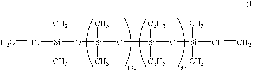
- a silicone base die-bonding material was prepared by intimately mixing 100 parts of a vinyl-terminated dimethyldiphenylpolysiloxane (viscosity 3 Pa.s) having formula (I), 2.5 parts of a methylhydrogenpolysiloxane (viscosity 15 mPa.s) having formula (II), 0.03 part of 2-ethylhexyl alcohol-modified chloroplatinic acid solution (Pt concentration 2 wt %), 0.05 part of ethynylcyclohexyl alcohol, 7 parts of 3-glycidoxypropyltrimethoxysilane, and 400 parts of spherical alumina fine powder having an average particle diameter of 9 ⁇ m.
- a light-emitting semiconductor device as shown in FIG. 1 was fabricated.
- An LED chip including an emissive layer of InGaN and having a main emission peak at 470 nm was used as a light-emitting member 2 .
- the light-emitting member 2 was secured to a housing 1 of glass fiber-reinforced epoxy resin having a pair of lead electrodes 3 and 4 , by using the silicone base die-bonding material 5 and heating at 180° C. for 10 minutes.
- Gold wires 6 were bonded to the light-emitting member 2 and the lead electrodes 3 and 4 for electrical connection.
- a potting composition 7 was cast into the interior of the housing 1 and cured at 180° C. for one hour, completing a light-emitting semiconductor device.
- a constant current flow was conducted across the light-emitting semiconductor device fabricated by the above potting method, whereby it emitted light toward a photo detector. After 5 seconds from the current conduction, the current output of the photo detector was measured as a measure of luminance. The luminance was reported as a relative value based on a luminance of 1.00 for the light-emitting semiconductor device of Example 1.
- a current flow of 20 mA was conducted across the light-emitting semiconductor device in a 150° C. atmosphere for 1,000 hours. Thereafter, room temperature was resumed, and a constant current flow was conducted across the light-emitting semiconductor device. After 5 seconds from the current conduction, the current output of the photo detector was measured. It was compared with the current output before the high-temperature current conduction, determining a luminance drop by heat degradation. The result was reported as a relative value based on the initial luminance of 1.00 for the light-emitting semiconductor device of Example 1.
- a silicone potting material was prepared by intimately mixing 100 parts of a vinyl-terminated dimethyldiphenylpolysiloxane (viscosity 3 Pa.s) having formula (I), 2.5 parts of a methylhydrogenpolysiloxane (viscosity 15 mPa.s) having formula (II), 0.03 part of 2-ethylhexyl alcohol-modified chloroplatinic acid solution (Pt concentration 2 wt %), 0.05 part of ethynylcyclohexyl alcohol, and 2 parts of an alkoxy-containing silicone compound having formula (III).
- the potting material cured into a silicone resin which had a Durometer type A hardness of 33 and a refractive index of 1.48 at 25° C. and 589 nm. Using the potting material, a light-emitting semiconductor device was fabricated as above.
- a silicone potting material was prepared by intimately mixing 100 parts of a vinyl-terminated dimethyldiphenylpolysiloxane (viscosity 5 Pa.s) having formula (IV), 7.0 parts of a methylhydrogenpolysiloxane (viscosity 90 mPa.s) having formula (V), 0.03 part of 2-ethylhexyl alcohol-modified chloroplatinic acid solution (Pt concentration 2 wt %), 0.05 part of ethynylcyclohexyl alcohol, and 3 parts of 3-methacryloxypropyltrimethoxysilane.
- the potting material cured into a silicone resin which had a Durometer type A hardness of 24 and a refractive index of 1.45 at 25° C. and 589 nm. Using the potting material, a light-emitting semiconductor device was fabricated as above.
- a silicone potting material was prepared by intimately mixing 100 parts of a vinyl-terminated dimethyldiphenylpolysiloxane (viscosity 2 Pa.s) having formula (VI), 4.1 parts of a phenylmethylhydrogenpolysiloxane (viscosity 30 mPa.s) having formula (VII), 0.03 part of 2-ethylhexyl alcohol-modified chloroplatinic acid solution (Pt concentration 2 wt %), 0.05 part of ethynylcyclohexyl alcohol, and 2 parts of an alkoxy-containing silicone compound having formula (VIII).
- the potting material cured into a silicone resin which had a Durometer type A hardness of 62 and a refractive index of 1.53 at 25° C. and 589 nm. Using the potting material, a light-emitting semiconductor device was fabricated as above.
- an organic solvent xylene
- a bisphenol A epoxy resin EP 827 by Yuka Shell Epoxy Co., Ltd.
- polydimethylsiloxane having two amino groups and a molecular weight of 1,680.
- the blend was heat treated at 150° C., after which the organic solvent was volatilized off, yielding a modified bisphenol A epoxy resin.
- 120 parts of the modified bisphenol A epoxy resin was blended with 100 parts of 4-methylhexahydrophthalic anhydride and 0.4 part of 2-ethyl-4-methylimidazole. They were intimately mixed to give an epoxy potting material.
- the epoxy potting material cured into a resin which had a Durometer type A hardness of 92 and a refractive index of 1.56 at 25° C. and 589 nm.
- a light-emitting semiconductor device was fabricated as above.
- a silicone potting material was prepared by intimately mixing 100 parts of a vinyl-terminated dimethylpolysiloxane (viscosity 3 Pa.s) having formula (IX), 2.0 parts of a methylhydrogenpolysiloxane (viscosity 15 mPa.s) having formula (II), 0.03 part of 2-ethylhexyl alcohol-modified chloroplatinic acid solution (Pt concentration 2 wt %), and 0.05 part of ethynylcyclohexyl alcohol.
- the potting material cured into a silicone resin which had a Durometer type A hardness of 58 and a refractive index of 1.40 at 25° C. and 589 nm. Using the potting material, a light-emitting semiconductor device was fabricated as above.
- a silicone potting material was prepared by intimately mixing 50 parts of a vinylmethylpolysiloxane of resin structure consisting of 50 mol % SiO 2 units, 42.5 mol % (CH 3 ) 3 SiO 0.5 units and 7.5 mol % Vi(CH 3 ) 2 SiO 0.5 units wherein Vi is vinyl, 50 parts of a vinyl-terminated dimethylpolysiloxane (viscosity 3 Pa.s) having formula (IX), 4.0 parts of a methylhydrogenpolysiloxane (viscosity 15 mPa.s) having formula (II), 0.03 part of 2-ethylhexyl alcohol-modified chloroplatinic acid solution (Pt concentration 2 wt %), and 0.05 part of ethynylcyclohexyl alcohol.
- the potting material cured into a silicone resin which had a Durometer type A hardness of 80 and a refractive index of 1.41 at 25° C. and 589 nm. Using the potting material, a light-emitting semiconductor device was fabricated as above.
- Table 1 shows the test results of the potting materials of Examples and Comparative Examples.
- Example Comparative Example 1 2 3 1 2 3 Resin hardness 33 24 62 92 58 80 Resin refractive 1.48 1.45 1.53 1.56 1.40 1.41 index Luminance* 1.00 1.00 1.06 1.10 0.65 0.70 Luminance drop by 0.99 0.98 1.02 0.12 0.65 0.68 current conduction* Thermal shock test 0/50 0/50 1/50 50/50 separated separated (cracked samples) 30/50 50/50 *relative value based on an initial luminance of 1.00 for the light-emitting semiconductor device of Example 1.
- the light-emitting semiconductor device in which the light-emitting semiconductor member is embedded and protected with the potting composition of the invention undergoes little discoloration and maintains a high emission efficiency in the heating tests.
- the invention that offers a light-emitting semiconductor device featuring a long life and energy saving is of great industrial worth.
Landscapes
- Chemical & Material Sciences (AREA)
- Health & Medical Sciences (AREA)
- Chemical Kinetics & Catalysis (AREA)
- Medicinal Chemistry (AREA)
- Polymers & Plastics (AREA)
- Organic Chemistry (AREA)
- Led Device Packages (AREA)
- Compositions Of Macromolecular Compounds (AREA)
- Structures Or Materials For Encapsulating Or Coating Semiconductor Devices Or Solid State Devices (AREA)
Abstract
Description


| TABLE 1 | ||
| Example | Comparative Example | |
| 1 | 2 | 3 | 1 | 2 | 3 | |
| Resin hardness | 33 | 24 | 62 | 92 | 58 | 80 |
| Resin refractive | 1.48 | 1.45 | 1.53 | 1.56 | 1.40 | 1.41 |
| index | ||||||
| Luminance* | 1.00 | 1.00 | 1.06 | 1.10 | 0.65 | 0.70 |
| Luminance drop by | 0.99 | 0.98 | 1.02 | 0.12 | 0.65 | 0.68 |
| current conduction* | ||||||
| Thermal shock test | 0/50 | 0/50 | 1/50 | 50/50 | separated | separated |
| (cracked samples) | 30/50 | 50/50 | ||||
| *relative value based on an initial luminance of 1.00 for the light-emitting semiconductor device of Example 1. | ||||||
Claims (5)
Applications Claiming Priority (2)
| Application Number | Priority Date | Filing Date | Title |
|---|---|---|---|
| JP2003066304 | 2003-03-12 | ||
| JP2003-066304 | 2003-03-12 |
Publications (2)
| Publication Number | Publication Date |
|---|---|
| US20040178509A1 US20040178509A1 (en) | 2004-09-16 |
| US6806509B2 true US6806509B2 (en) | 2004-10-19 |
Family
ID=32959242
Family Applications (1)
| Application Number | Title | Priority Date | Filing Date |
|---|---|---|---|
| US10/797,139 Expired - Lifetime US6806509B2 (en) | 2003-03-12 | 2004-03-11 | Light-emitting semiconductor potting composition and light-emitting semiconductor device |
Country Status (3)
| Country | Link |
|---|---|
| US (1) | US6806509B2 (en) |
| JP (1) | JP2010174250A (en) |
| TW (1) | TW200427111A (en) |
Cited By (56)
| Publication number | Priority date | Publication date | Assignee | Title |
|---|---|---|---|---|
| US20050173708A1 (en) * | 2004-02-06 | 2005-08-11 | Toyoda Gosei Co., Ltd. | Light emitting device and sealing material |
| US20050244649A1 (en) * | 2004-04-30 | 2005-11-03 | Shin-Etsu Chemical Co., Ltd. | Epoxy-silicone mixed resin composition and light-emitting semiconductor device |
| US20060105481A1 (en) * | 2004-11-18 | 2006-05-18 | 3M Innovative Properties Company | Method of making light emitting device with silicon-containing encapsulant |
| US20060105480A1 (en) * | 2004-11-18 | 2006-05-18 | Boardman Larry D | Method of making light emitting device with silicon-containing encapsulant |
| US20060134440A1 (en) * | 2004-10-27 | 2006-06-22 | Crivello James V | Silicone encapsulants for light emitting diodes |
| US20060159937A1 (en) * | 2005-01-20 | 2006-07-20 | Shin-Etsu Chemical Co., Ltd. | Silicone-sealed LED |
| US20060235142A1 (en) * | 2003-10-10 | 2006-10-19 | Hostman John B | Carbinol functional silicone resins |
| US20070092636A1 (en) * | 2005-10-24 | 2007-04-26 | 3M Innovative Properties Company | Method of making light emitting device having a molded encapsulant |
| US20070092736A1 (en) * | 2005-10-21 | 2007-04-26 | 3M Innovative Properties Company | Method of making light emitting device with silicon-containing encapsulant |
| US20070092737A1 (en) * | 2005-10-21 | 2007-04-26 | 3M Innovative Properties Company | Method of making light emitting device with silicon-containing encapsulant |
| US20070197742A1 (en) * | 2006-02-20 | 2007-08-23 | Shin-Etsu Chemical Co., Ltd. | Heat curable silicone composition |
| US20070269586A1 (en) * | 2006-05-17 | 2007-11-22 | 3M Innovative Properties Company | Method of making light emitting device with silicon-containing composition |
| US20070287208A1 (en) * | 2006-05-17 | 2007-12-13 | 3M Innovative Properties Company | Method of Making Light Emitting Device With Multilayer Silicon-Containing Encapsulant |
| US20070293623A1 (en) * | 2006-06-14 | 2007-12-20 | Shin-Etsu Chemical Co., Ltd | Phosphor-filled curable silicone resin composition and cured product thereof |
| US20080027200A1 (en) * | 2006-07-26 | 2008-01-31 | Shin -Etsu Chemical Co., Ltd. | Phosphor-containing curable silicone composition for led and led light-emitting device using the composition |
| US20080079182A1 (en) * | 2006-08-17 | 2008-04-03 | 3M Innovative Properties Company | Method of making a light emitting device having a molded encapsulant |
| US20080090986A1 (en) * | 2006-10-16 | 2008-04-17 | Garo Khanarian | Heat stable aryl polysiloxane compositions |
| WO2008063884A1 (en) * | 2006-11-20 | 2008-05-29 | 3M Innovative Properties Company | Optical bonding composition for led light source |
| WO2008064070A1 (en) * | 2006-11-17 | 2008-05-29 | 3M Innovative Properties Company | Optical bonding composition for led light source |
| US20080185601A1 (en) * | 2005-05-26 | 2008-08-07 | Lawrence Frisch | Process and Silicone Encapsulant Composition for Molding Small Shapes |
| US20080203415A1 (en) * | 2007-02-13 | 2008-08-28 | 3M Innovative Properties Company | Led devices having lenses and methods of making same |
| US20080207078A1 (en) * | 2005-08-04 | 2008-08-28 | Taiwan Oasis Technology Co., Ltd. | Multi-wavelength LED construction & manufacturing proces |
| US20080210948A1 (en) * | 2004-09-06 | 2008-09-04 | The Kansai Electric Power Co., Inc. | High-Heat-Resistive Semiconductor Device |
| US20090003758A1 (en) * | 2006-02-01 | 2009-01-01 | Jon Degroot | Impact Resistant Optical Waveguide and Method of Manufacture Thereof |
| US20090076184A1 (en) * | 2007-09-14 | 2009-03-19 | 3M Innovative Properties Company | Light emitting device having silicon-containing composition and method of making same |
| US20090146175A1 (en) * | 2006-01-17 | 2009-06-11 | Maneesh Bahadur | Thermal stable transparent silicone resin compositions and methods for their preparation and use |
| US20090171013A1 (en) * | 2007-12-26 | 2009-07-02 | Taguchi Yusuke | White heat-curable silicone resin composition, optoelectronic part case, and molding method |
| US20090239997A1 (en) * | 2008-03-18 | 2009-09-24 | Taguchi Yusuke | White thermosetting silicone resin composition for molding an optical semiconductor case and optical semiconductor case |
| US7595515B2 (en) | 2005-10-24 | 2009-09-29 | 3M Innovative Properties Company | Method of making light emitting device having a molded encapsulant |
| US20090304961A1 (en) * | 2008-06-09 | 2009-12-10 | Taguchi Yusuke | White heat-curable silicone resin composition and optoelectronic part case |
| US20090306263A1 (en) * | 2008-06-09 | 2009-12-10 | Taguchi Yusuke | White heat-curable silicone resin composition and optoelectronic part case |
| US20100048140A1 (en) * | 2006-11-20 | 2010-02-25 | Toyota Jidosha Kabushiki Kaisha | Device for measuring a position of a mobile station |
| US20100051970A1 (en) * | 2006-11-17 | 2010-03-04 | Ouderkirk Andrew J | Planarized led with optical extractor |
| US20100078581A1 (en) * | 2008-09-29 | 2010-04-01 | Scully Signal Company | Fluid overfill probe with thermal stress prevention |
| RU2401846C2 (en) * | 2006-04-25 | 2010-10-20 | Учреждение Российской академии наук Институт синтетических полимерных материалов им. Н.С. Ениколопова РАН (ИСПМ РАН) | Functional polyorganosiloxanes and curable composition based on said polyorganosiloxanes |
| US20100276721A1 (en) * | 2006-02-24 | 2010-11-04 | Dow Corning Corporation | Light Emitting Device Encapsulated with Silicones and Curable Silicone Compositions for Preparing the Silicones |
| RU2427592C2 (en) * | 2007-04-24 | 2011-08-27 | Учреждение Российской академии наук Институт синтетических полимерных материалов им. Н.С. Ениколопова РАН (ИСПМ) | Method of producing functional polyorganosiloxanes and composition based thereon |
| US20110215707A1 (en) * | 2010-03-03 | 2011-09-08 | LumenFlow Corp. | Constrained folded path resonant white light scintillator |
| US20110227235A1 (en) * | 2008-09-05 | 2011-09-22 | Makoto Yoshitake | Curable Organopolysiloxane Composition, Optical Semiconductor Element Sealant, and Optical Semiconductor Device |
| US8044412B2 (en) | 2006-01-20 | 2011-10-25 | Taiwan Semiconductor Manufacturing Company, Ltd | Package for a light emitting element |
| US8071987B2 (en) | 2006-09-29 | 2011-12-06 | Osram Opto Semiconductors Gmbh | Housing for an optoelectronic component, optoelectronic component, and method for producing a housing for an optoelectronic component |
| US20120068560A1 (en) * | 2010-09-22 | 2012-03-22 | Alstom Technology Ltd | Arrangement of conducting bar ends |
| US20130082369A1 (en) * | 2010-04-02 | 2013-04-04 | Kaneka Corporation | Curable resin composition, curable resin composition tablet, molded body, semiconductor package, semiconductor component and light emitting diode |
| US20140103546A1 (en) * | 2012-10-16 | 2014-04-17 | Brewer Science Inc. | Silicone polymers with high refractive indices and extended pot life |
| US8759468B2 (en) | 2011-05-11 | 2014-06-24 | Henkel (China) Company Limited | Silicone resin with improved barrier properties |
| US20140175505A1 (en) * | 2011-07-14 | 2014-06-26 | Ryosuke Yamazaki | Sealing agent for optical semiconductor devices, and optical semiconductor device |
| US20140367723A1 (en) * | 2012-02-02 | 2014-12-18 | Dow Corning Toray Co., Ltd. | Curable Silicone Composition, Cured Product Thereof, And Optical Semiconductor Device |
| US8946353B2 (en) | 2008-10-31 | 2015-02-03 | Dow Corning Toray Co. Ltd. | Curable organopolysiloxane composition, optical semiconductor element sealant, and optical semiconductor device |
| US20150353733A1 (en) * | 2014-06-06 | 2015-12-10 | Shin-Etsu Chemical Co., Ltd. | White thermosetting silicone resin composition for a light-emitting semiconductor device and a case for installing a light-emitting semiconductor element |
| WO2016151192A1 (en) | 2015-03-20 | 2016-09-29 | Inkron Oy | High-ri siloxane monomers, their polymerization and use |
| US9540488B1 (en) | 2015-12-16 | 2017-01-10 | Industrial Technology Research Institute | Siloxane resin composition, and photoelectric device employing the same |
| WO2018011475A1 (en) | 2016-07-14 | 2018-01-18 | Inkron Oy | Siloxane monomers, their polymerization and uses thereof |
| US9944031B2 (en) | 2007-02-13 | 2018-04-17 | 3M Innovative Properties Company | Molded optical articles and methods of making same |
| US10115714B2 (en) | 2015-09-04 | 2018-10-30 | Kabushiki Kaisha Toshiba | Semiconductor device and optical coupling device |
| US20200197551A1 (en) * | 2012-08-28 | 2020-06-25 | Sensor Electronic Technology, Inc. | Ultraviolet Gradient Sterilization, Disinfection, and Storage System |
| US11773222B2 (en) | 2021-08-25 | 2023-10-03 | Industrial Technology Research Institute | Curable composition and electronic device employing the same |
Families Citing this family (26)
| Publication number | Priority date | Publication date | Assignee | Title |
|---|---|---|---|---|
| CN100444371C (en) | 2004-09-13 | 2008-12-17 | 国际整流器公司 | Power Semiconductor Packaging |
| CN100416871C (en) * | 2004-12-09 | 2008-09-03 | 璨圆光电股份有限公司 | Light emitting diode packaging structure |
| JP5705396B2 (en) * | 2005-01-24 | 2015-04-22 | モメンティブ・パフォーマンス・マテリアルズ・ジャパン合同会社 | Silicone composition for sealing light emitting device and light emitting device |
| JP4648099B2 (en) * | 2005-06-07 | 2011-03-09 | 信越化学工業株式会社 | Silicone resin composition for die bonding |
| KR100665375B1 (en) * | 2006-02-22 | 2007-01-09 | 삼성전기주식회사 | LED Package |
| WO2007135707A1 (en) | 2006-05-18 | 2007-11-29 | Nichia Corporation | Resin molded body and surface-mounted light emitting device, and manufacturing method thereof |
| US20090065792A1 (en) | 2007-09-07 | 2009-03-12 | 3M Innovative Properties Company | Method of making an led device having a dome lens |
| CN100490201C (en) * | 2007-12-20 | 2009-05-20 | 宁波安迪光电科技有限公司 | White light LED |
| JP5136963B2 (en) * | 2008-03-24 | 2013-02-06 | 信越化学工業株式会社 | Curable silicone rubber composition and semiconductor device |
| JP4862032B2 (en) * | 2008-12-05 | 2012-01-25 | 信越化学工業株式会社 | Addition-curable silicone composition that provides a cured product having a high refractive index, and an optical element sealing material comprising the composition |
| JP5746227B2 (en) | 2010-03-05 | 2015-07-08 | モメンティブ パフォーマンス マテリアルズ ゲーエムベーハー | Curable polyorganosiloxane composition for use as a sealant for solar cell modules |
| JP2011219597A (en) * | 2010-04-08 | 2011-11-04 | Nitto Denko Corp | Silicone resin sheet |
| JP2012052035A (en) * | 2010-09-01 | 2012-03-15 | Shin-Etsu Chemical Co Ltd | Addition-curable silicone composition, optical element encapsulating material comprising the composition, and semiconductor device in which optical element is encapsulated with cured product of the optical element encapsulating material |
| JP2012074512A (en) * | 2010-09-28 | 2012-04-12 | Sekisui Chem Co Ltd | Die-bonding material for optical semiconductor device and optical semiconductor device using the same |
| KR101472829B1 (en) * | 2011-04-21 | 2014-12-15 | 제이에스알 가부시끼가이샤 | Curable composition, cured product, photo-semiconductor device, and polysiloxane |
| JP5575820B2 (en) * | 2012-01-31 | 2014-08-20 | 信越化学工業株式会社 | Curable organopolysiloxane composition, optical element sealing material, and optical element |
| KR102071013B1 (en) | 2012-05-14 | 2020-01-29 | 모멘티브 퍼포먼스 머티리얼즈 인크. | High refractive index material |
| US9287475B2 (en) * | 2012-07-20 | 2016-03-15 | Cree, Inc. | Solid state lighting component package with reflective polymer matrix layer |
| JP6006632B2 (en) | 2012-12-18 | 2016-10-12 | 信越化学工業株式会社 | Addition-curing silicone composition and optical element |
| CN103724939A (en) * | 2013-12-26 | 2014-04-16 | 东莞市广海大橡塑科技有限公司 | Packaged diode |
| JPWO2015115341A1 (en) * | 2014-01-31 | 2017-03-23 | 住友化学株式会社 | Manufacturing method of semiconductor light emitting device |
| JP6100717B2 (en) | 2014-03-05 | 2017-03-22 | 信越化学工業株式会社 | Addition-curing silicone composition and optical element |
| CN105199397B (en) * | 2014-06-17 | 2018-05-08 | 广州慧谷化学有限公司 | A kind of curable organopolysiloxane composition and semiconductor devices |
| JP6751368B2 (en) * | 2017-04-27 | 2020-09-02 | 信越化学工業株式会社 | Addition-curable silicone composition, method for producing the composition, and optical semiconductor device |
| JP7090842B2 (en) * | 2017-07-27 | 2022-06-27 | 日本電気硝子株式会社 | Wavelength conversion member and light emitting device |
| CN114088557B (en) * | 2021-12-31 | 2023-07-07 | 广东皓明有机硅材料有限公司 | Method for testing poisoning resistance of addition type organic silicon pouring sealant and application thereof |
Citations (11)
| Publication number | Priority date | Publication date | Assignee | Title |
|---|---|---|---|---|
| US4741861A (en) * | 1985-02-25 | 1988-05-03 | Shin-Etsu Chemical Co., Ltd. | Silicone-based antifoam composition and a method for the preparation of the same |
| US5314979A (en) * | 1990-12-10 | 1994-05-24 | Shin-Etsu Chemical Co., Ltd. | Optical fibers and core - forming compositions |
| JPH0725987A (en) | 1993-07-14 | 1995-01-27 | Nitto Denko Corp | Epoxy resin composition for optical semiconductor encapsulation |
| JPH11274571A (en) | 1998-01-26 | 1999-10-08 | Nichia Chem Ind Ltd | Semiconductor light emitting device |
| US6010646A (en) * | 1997-04-11 | 2000-01-04 | Potters Industries, Inc. | Electroconductive composition and methods for producing such composition |
| JP2001217467A (en) | 2000-02-02 | 2001-08-10 | Ind Technol Res Inst | High efficiency white light emitting diode |
| US6403226B1 (en) * | 1996-05-17 | 2002-06-11 | 3M Innovative Properties Company | Electronic assemblies with elastomeric members made from cured, room temperature curable silicone compositions having improved stress relaxation resistance |
| US20020145152A1 (en) | 2001-04-09 | 2002-10-10 | Kabushiki Kaisha Toshiba | Light emitting device |
| JP2002314143A (en) | 2001-04-09 | 2002-10-25 | Toshiba Corp | Light emitting device |
| JP2002327126A (en) | 2001-02-23 | 2002-11-15 | Kanegafuchi Chem Ind Co Ltd | Composition for optical material, optical material, method for producing the same, liquid crystal display device and light emitting diode using the same |
| JP2002338833A (en) | 2001-02-23 | 2002-11-27 | Kanegafuchi Chem Ind Co Ltd | Composition for optical material, optical material, method for producing the same, liquid crystal display device and light emitting diode using the same |
Family Cites Families (6)
| Publication number | Priority date | Publication date | Assignee | Title |
|---|---|---|---|---|
| JPH03766A (en) * | 1989-05-30 | 1991-01-07 | Toshiba Silicone Co Ltd | Polyorganosiloxane composition |
| JP3615784B2 (en) * | 1994-04-21 | 2005-02-02 | ダウ コーニング アジア株式会社 | Resin composition for optical element and optical element |
| JP3922785B2 (en) * | 1998-02-09 | 2007-05-30 | モメンティブ・パフォーマンス・マテリアルズ・ジャパン合同会社 | Optical semiconductor insulation coating protective agent |
| JP4040858B2 (en) * | 2001-10-19 | 2008-01-30 | 東レ・ダウコーニング株式会社 | Curable organopolysiloxane composition and semiconductor device |
| JP4409160B2 (en) * | 2002-10-28 | 2010-02-03 | 東レ・ダウコーニング株式会社 | Curable organopolysiloxane composition and semiconductor device |
| JP4766222B2 (en) * | 2003-03-12 | 2011-09-07 | 信越化学工業株式会社 | Light emitting semiconductor coating protective material and light emitting semiconductor device |
-
2004
- 2004-03-08 TW TW093106063A patent/TW200427111A/en not_active IP Right Cessation
- 2004-03-11 US US10/797,139 patent/US6806509B2/en not_active Expired - Lifetime
-
2010
- 2010-03-19 JP JP2010064144A patent/JP2010174250A/en active Pending
Patent Citations (14)
| Publication number | Priority date | Publication date | Assignee | Title |
|---|---|---|---|---|
| US4741861A (en) * | 1985-02-25 | 1988-05-03 | Shin-Etsu Chemical Co., Ltd. | Silicone-based antifoam composition and a method for the preparation of the same |
| US5314979A (en) * | 1990-12-10 | 1994-05-24 | Shin-Etsu Chemical Co., Ltd. | Optical fibers and core - forming compositions |
| JPH0725987A (en) | 1993-07-14 | 1995-01-27 | Nitto Denko Corp | Epoxy resin composition for optical semiconductor encapsulation |
| US6403226B1 (en) * | 1996-05-17 | 2002-06-11 | 3M Innovative Properties Company | Electronic assemblies with elastomeric members made from cured, room temperature curable silicone compositions having improved stress relaxation resistance |
| US6010646A (en) * | 1997-04-11 | 2000-01-04 | Potters Industries, Inc. | Electroconductive composition and methods for producing such composition |
| JPH11274571A (en) | 1998-01-26 | 1999-10-08 | Nichia Chem Ind Ltd | Semiconductor light emitting device |
| JP2001217467A (en) | 2000-02-02 | 2001-08-10 | Ind Technol Res Inst | High efficiency white light emitting diode |
| US6614172B2 (en) | 2000-02-02 | 2003-09-02 | Industrial Technology Research Institute | High efficiency white light emitting diode |
| JP2002327126A (en) | 2001-02-23 | 2002-11-15 | Kanegafuchi Chem Ind Co Ltd | Composition for optical material, optical material, method for producing the same, liquid crystal display device and light emitting diode using the same |
| JP2002338833A (en) | 2001-02-23 | 2002-11-27 | Kanegafuchi Chem Ind Co Ltd | Composition for optical material, optical material, method for producing the same, liquid crystal display device and light emitting diode using the same |
| US20020145152A1 (en) | 2001-04-09 | 2002-10-10 | Kabushiki Kaisha Toshiba | Light emitting device |
| JP2002314143A (en) | 2001-04-09 | 2002-10-25 | Toshiba Corp | Light emitting device |
| JP2002314139A (en) | 2001-04-09 | 2002-10-25 | Toshiba Corp | Light emitting device |
| US20020190262A1 (en) | 2001-04-09 | 2002-12-19 | Koichi Nitta | Light emitting device |
Cited By (111)
| Publication number | Priority date | Publication date | Assignee | Title |
|---|---|---|---|---|
| US7858697B2 (en) * | 2003-10-10 | 2010-12-28 | Dow Corning Corporation | Carbinol functional silicone resins |
| US20060235142A1 (en) * | 2003-10-10 | 2006-10-19 | Hostman John B | Carbinol functional silicone resins |
| US7304326B2 (en) * | 2004-02-06 | 2007-12-04 | Toyoda Gosei Co., Ltd. | Light emitting device and sealing material |
| US20050173708A1 (en) * | 2004-02-06 | 2005-08-11 | Toyoda Gosei Co., Ltd. | Light emitting device and sealing material |
| US20050244649A1 (en) * | 2004-04-30 | 2005-11-03 | Shin-Etsu Chemical Co., Ltd. | Epoxy-silicone mixed resin composition and light-emitting semiconductor device |
| US7276562B2 (en) * | 2004-04-30 | 2007-10-02 | Shin-Etsu Chemical Co., Ltd. | Epoxy-silicone mixed resin composition and light-emitting semiconductor device |
| US7772594B2 (en) * | 2004-09-06 | 2010-08-10 | The Kansai Electric Power Co., Inc. | High-heat-resistive semiconductor device |
| US20080210948A1 (en) * | 2004-09-06 | 2008-09-04 | The Kansai Electric Power Co., Inc. | High-Heat-Resistive Semiconductor Device |
| US20060134440A1 (en) * | 2004-10-27 | 2006-06-22 | Crivello James V | Silicone encapsulants for light emitting diodes |
| TWI401817B (en) * | 2004-11-18 | 2013-07-11 | 3M新設資產公司 | Method for manufacturing illuminating device with enamel sealing material |
| US7314770B2 (en) * | 2004-11-18 | 2008-01-01 | 3M Innovative Properties Company | Method of making light emitting device with silicon-containing encapsulant |
| US7192795B2 (en) | 2004-11-18 | 2007-03-20 | 3M Innovative Properties Company | Method of making light emitting device with silicon-containing encapsulant |
| US20060199291A1 (en) * | 2004-11-18 | 2006-09-07 | 3M Innovative Properties Company | Method of making light emitting device with silicon-containing encapsulant |
| US7427523B2 (en) | 2004-11-18 | 2008-09-23 | 3M Innovative Properties Company | Method of making light emitting device with silicon-containing encapsulant |
| US20060105480A1 (en) * | 2004-11-18 | 2006-05-18 | Boardman Larry D | Method of making light emitting device with silicon-containing encapsulant |
| CN100546057C (en) * | 2004-11-18 | 2009-09-30 | 3M创新有限公司 | Method for manufacturing light emitting device using silicon-containing sealant and light emitting device manufactured using the same |
| US20060105481A1 (en) * | 2004-11-18 | 2006-05-18 | 3M Innovative Properties Company | Method of making light emitting device with silicon-containing encapsulant |
| US20060159937A1 (en) * | 2005-01-20 | 2006-07-20 | Shin-Etsu Chemical Co., Ltd. | Silicone-sealed LED |
| US7838117B2 (en) * | 2005-01-20 | 2010-11-23 | Shin-Etsu Chemical Co., Ltd. | Silicone-sealed LED |
| US8071697B2 (en) | 2005-05-26 | 2011-12-06 | Dow Corning Corporation | Silicone encapsulant composition for molding small shapes |
| US20080185601A1 (en) * | 2005-05-26 | 2008-08-07 | Lawrence Frisch | Process and Silicone Encapsulant Composition for Molding Small Shapes |
| US20080207078A1 (en) * | 2005-08-04 | 2008-08-28 | Taiwan Oasis Technology Co., Ltd. | Multi-wavelength LED construction & manufacturing proces |
| US20070092736A1 (en) * | 2005-10-21 | 2007-04-26 | 3M Innovative Properties Company | Method of making light emitting device with silicon-containing encapsulant |
| US20070092737A1 (en) * | 2005-10-21 | 2007-04-26 | 3M Innovative Properties Company | Method of making light emitting device with silicon-containing encapsulant |
| EP1949459A4 (en) * | 2005-10-24 | 2014-04-30 | 3M Innovative Properties Co | METHOD FOR MANUFACTURING A LIGHT EMITTING DEVICE COMPRISING A MOLDED ENCAPSULANT |
| TWI415289B (en) * | 2005-10-24 | 2013-11-11 | 3M新設資產公司 | Method of manufacturing a light-emitting device having a molded package |
| US7595515B2 (en) | 2005-10-24 | 2009-09-29 | 3M Innovative Properties Company | Method of making light emitting device having a molded encapsulant |
| US20070092636A1 (en) * | 2005-10-24 | 2007-04-26 | 3M Innovative Properties Company | Method of making light emitting device having a molded encapsulant |
| KR101278415B1 (en) * | 2005-10-24 | 2013-06-24 | 쓰리엠 이노베이티브 프로퍼티즈 컴파니 | Method of making light emitting device having a molded encapsulant |
| JP2009513021A (en) * | 2005-10-24 | 2009-03-26 | スリーエム イノベイティブ プロパティズ カンパニー | Method of manufacturing light emitting device having molded encapsulant |
| US20090146175A1 (en) * | 2006-01-17 | 2009-06-11 | Maneesh Bahadur | Thermal stable transparent silicone resin compositions and methods for their preparation and use |
| US8044412B2 (en) | 2006-01-20 | 2011-10-25 | Taiwan Semiconductor Manufacturing Company, Ltd | Package for a light emitting element |
| US8552460B2 (en) | 2006-01-20 | 2013-10-08 | Tsmc Solid State Lighting Ltd. | Package for a light emitting element |
| US20090003758A1 (en) * | 2006-02-01 | 2009-01-01 | Jon Degroot | Impact Resistant Optical Waveguide and Method of Manufacture Thereof |
| US7551830B2 (en) | 2006-02-01 | 2009-06-23 | Dow Corning Corporation | Impact resistant optical waveguide and method of manufacture thereof |
| US20070197742A1 (en) * | 2006-02-20 | 2007-08-23 | Shin-Etsu Chemical Co., Ltd. | Heat curable silicone composition |
| US8258502B2 (en) | 2006-02-24 | 2012-09-04 | Dow Corning Corporation | Light emitting device encapsulated with silicones and curable silicone compositions for preparing the silicones |
| US20100276721A1 (en) * | 2006-02-24 | 2010-11-04 | Dow Corning Corporation | Light Emitting Device Encapsulated with Silicones and Curable Silicone Compositions for Preparing the Silicones |
| RU2401846C2 (en) * | 2006-04-25 | 2010-10-20 | Учреждение Российской академии наук Институт синтетических полимерных материалов им. Н.С. Ениколопова РАН (ИСПМ РАН) | Functional polyorganosiloxanes and curable composition based on said polyorganosiloxanes |
| WO2007136956A1 (en) * | 2006-05-17 | 2007-11-29 | 3M Innovative Properties Company | Method of making light emitting device with silicon-containing composition |
| US7655486B2 (en) | 2006-05-17 | 2010-02-02 | 3M Innovative Properties Company | Method of making light emitting device with multilayer silicon-containing encapsulant |
| US9308680B2 (en) | 2006-05-17 | 2016-04-12 | 3M Innovative Properties Company | Light emitting device with multilayer silicon-containing encapsulant |
| CN101443926B (en) * | 2006-05-17 | 2012-05-30 | 3M创新有限公司 | Method for preparing light-emitting device using silicon-containing composition |
| US20100133574A1 (en) * | 2006-05-17 | 2010-06-03 | 3M Innovative Properties Company | Light emitting device with multilayer silicon-containing encapsulant |
| US20070269586A1 (en) * | 2006-05-17 | 2007-11-22 | 3M Innovative Properties Company | Method of making light emitting device with silicon-containing composition |
| US20070287208A1 (en) * | 2006-05-17 | 2007-12-13 | 3M Innovative Properties Company | Method of Making Light Emitting Device With Multilayer Silicon-Containing Encapsulant |
| US7705093B2 (en) * | 2006-06-14 | 2010-04-27 | Shin-Etsu Chemical Co., Ltd. | Phosphor-filled curable silicone resin composition and cured product thereof |
| US20070293623A1 (en) * | 2006-06-14 | 2007-12-20 | Shin-Etsu Chemical Co., Ltd | Phosphor-filled curable silicone resin composition and cured product thereof |
| US20080027200A1 (en) * | 2006-07-26 | 2008-01-31 | Shin -Etsu Chemical Co., Ltd. | Phosphor-containing curable silicone composition for led and led light-emitting device using the composition |
| US8303878B2 (en) | 2006-08-17 | 2012-11-06 | 3M Innovative Properties Company | Method of making a light emitting device having a molded encapsulant |
| US20080079182A1 (en) * | 2006-08-17 | 2008-04-03 | 3M Innovative Properties Company | Method of making a light emitting device having a molded encapsulant |
| US8092735B2 (en) | 2006-08-17 | 2012-01-10 | 3M Innovative Properties Company | Method of making a light emitting device having a molded encapsulant |
| US8071987B2 (en) | 2006-09-29 | 2011-12-06 | Osram Opto Semiconductors Gmbh | Housing for an optoelectronic component, optoelectronic component, and method for producing a housing for an optoelectronic component |
| US8476114B2 (en) | 2006-09-29 | 2013-07-02 | Osram Opto Semiconductors Gmbh | Housing for an optoelectronic component, optoelectronic component, and method for producing a housing for an optoelectronic component |
| US20080090986A1 (en) * | 2006-10-16 | 2008-04-17 | Garo Khanarian | Heat stable aryl polysiloxane compositions |
| US8142895B2 (en) | 2006-10-16 | 2012-03-27 | Rohm And Haas Company | Heat stable aryl polysiloxane compositions |
| US20100059776A1 (en) * | 2006-11-17 | 2010-03-11 | 3M Innovative Properties Company | Optical bonding composition for led light source |
| WO2008064070A1 (en) * | 2006-11-17 | 2008-05-29 | 3M Innovative Properties Company | Optical bonding composition for led light source |
| US8026115B2 (en) | 2006-11-17 | 2011-09-27 | 3M Innovative Properties Company | Optical bonding composition for LED light source |
| US20100051970A1 (en) * | 2006-11-17 | 2010-03-04 | Ouderkirk Andrew J | Planarized led with optical extractor |
| WO2008063884A1 (en) * | 2006-11-20 | 2008-05-29 | 3M Innovative Properties Company | Optical bonding composition for led light source |
| US8013345B2 (en) | 2006-11-20 | 2011-09-06 | 3M Innovative Properties Company | Optical bonding composition for LED light source |
| US20100025711A1 (en) * | 2006-11-20 | 2010-02-04 | Barnes Amy S | Optical bonding composition for led light source |
| US20100048140A1 (en) * | 2006-11-20 | 2010-02-25 | Toyota Jidosha Kabushiki Kaisha | Device for measuring a position of a mobile station |
| US20080203415A1 (en) * | 2007-02-13 | 2008-08-28 | 3M Innovative Properties Company | Led devices having lenses and methods of making same |
| US9944031B2 (en) | 2007-02-13 | 2018-04-17 | 3M Innovative Properties Company | Molded optical articles and methods of making same |
| US8330176B2 (en) | 2007-02-13 | 2012-12-11 | 3M Innovative Properties Company | LED devices having lenses and methods of making same |
| US8901588B2 (en) | 2007-02-13 | 2014-12-02 | 3M Innovative Properties Company | LED devices having lenses and methods of making same |
| RU2427592C2 (en) * | 2007-04-24 | 2011-08-27 | Учреждение Российской академии наук Институт синтетических полимерных материалов им. Н.С. Ениколопова РАН (ИСПМ) | Method of producing functional polyorganosiloxanes and composition based thereon |
| US7960192B2 (en) | 2007-09-14 | 2011-06-14 | 3M Innovative Properties Company | Light emitting device having silicon-containing composition and method of making same |
| US20090076184A1 (en) * | 2007-09-14 | 2009-03-19 | 3M Innovative Properties Company | Light emitting device having silicon-containing composition and method of making same |
| KR101505626B1 (en) | 2007-12-26 | 2015-03-24 | 신에쓰 가가꾸 고교 가부시끼가이샤 | White thermosetting silicone resin composition for optical semiconductor case formation and optical semiconductor case and molding method thereof |
| US8013056B2 (en) * | 2007-12-26 | 2011-09-06 | Shin-Etsu Chemical Co., Ltd. | White heat-curable silicone resin composition, optoelectronic part case, and molding method |
| US20090171013A1 (en) * | 2007-12-26 | 2009-07-02 | Taguchi Yusuke | White heat-curable silicone resin composition, optoelectronic part case, and molding method |
| US8013057B2 (en) * | 2008-03-18 | 2011-09-06 | Shin-Etsu Chemical Co., Ltd. | White thermosetting silicone resin composition for molding an optical semiconductor case and optical semiconductor case |
| US20090239997A1 (en) * | 2008-03-18 | 2009-09-24 | Taguchi Yusuke | White thermosetting silicone resin composition for molding an optical semiconductor case and optical semiconductor case |
| US20090306263A1 (en) * | 2008-06-09 | 2009-12-10 | Taguchi Yusuke | White heat-curable silicone resin composition and optoelectronic part case |
| US20090304961A1 (en) * | 2008-06-09 | 2009-12-10 | Taguchi Yusuke | White heat-curable silicone resin composition and optoelectronic part case |
| US8012381B2 (en) * | 2008-06-09 | 2011-09-06 | Shin-Etsu Chemical Co., Ltd. | White heat-curable silicone resin composition and optoelectronic part case |
| US8173053B2 (en) * | 2008-06-09 | 2012-05-08 | Shin-Etsu Chemical Co., Ltd. | White heat-curable silicone resin composition and optoelectronic part case |
| US8373286B2 (en) | 2008-09-05 | 2013-02-12 | Dow Corning Toray Co., Ltd. | Curable organopolysiloxane composition, optical semiconductor element sealant, and optical semiconductor device |
| US20110227235A1 (en) * | 2008-09-05 | 2011-09-22 | Makoto Yoshitake | Curable Organopolysiloxane Composition, Optical Semiconductor Element Sealant, and Optical Semiconductor Device |
| US20100078581A1 (en) * | 2008-09-29 | 2010-04-01 | Scully Signal Company | Fluid overfill probe with thermal stress prevention |
| US7838859B2 (en) | 2008-09-29 | 2010-11-23 | Scully Signal Company | Fluid overfill probe with thermal stress prevention |
| US8946353B2 (en) | 2008-10-31 | 2015-02-03 | Dow Corning Toray Co. Ltd. | Curable organopolysiloxane composition, optical semiconductor element sealant, and optical semiconductor device |
| US8646949B2 (en) | 2010-03-03 | 2014-02-11 | LumenFlow Corp. | Constrained folded path resonant white light scintillator |
| US20110215707A1 (en) * | 2010-03-03 | 2011-09-08 | LumenFlow Corp. | Constrained folded path resonant white light scintillator |
| US20130082369A1 (en) * | 2010-04-02 | 2013-04-04 | Kaneka Corporation | Curable resin composition, curable resin composition tablet, molded body, semiconductor package, semiconductor component and light emitting diode |
| US9178120B2 (en) * | 2010-04-02 | 2015-11-03 | Kaneka Corporation | Curable resin composition, curable resin composition tablet, molded body, semiconductor package, semiconductor component and light emitting diode |
| US9496468B2 (en) | 2010-04-02 | 2016-11-15 | Kaneka Corporation | Curable resin composition, curable resin composition tablet, molded body, semiconductor package, semiconductor component and light emitting diode |
| US9257878B2 (en) * | 2010-09-22 | 2016-02-09 | Alstom Technology Ltd. | Arrangement of conducting bar ends |
| US20120068560A1 (en) * | 2010-09-22 | 2012-03-22 | Alstom Technology Ltd | Arrangement of conducting bar ends |
| US8759468B2 (en) | 2011-05-11 | 2014-06-24 | Henkel (China) Company Limited | Silicone resin with improved barrier properties |
| US20140175505A1 (en) * | 2011-07-14 | 2014-06-26 | Ryosuke Yamazaki | Sealing agent for optical semiconductor devices, and optical semiconductor device |
| US20140367723A1 (en) * | 2012-02-02 | 2014-12-18 | Dow Corning Toray Co., Ltd. | Curable Silicone Composition, Cured Product Thereof, And Optical Semiconductor Device |
| US9048406B2 (en) * | 2012-02-02 | 2015-06-02 | Dow Corning Toray Co., Ltd. | Curable silicone composition, cured product thereof, and optical semiconductor device |
| US20200197551A1 (en) * | 2012-08-28 | 2020-06-25 | Sensor Electronic Technology, Inc. | Ultraviolet Gradient Sterilization, Disinfection, and Storage System |
| US20140103546A1 (en) * | 2012-10-16 | 2014-04-17 | Brewer Science Inc. | Silicone polymers with high refractive indices and extended pot life |
| US9117757B2 (en) * | 2012-10-16 | 2015-08-25 | Brewer Science Inc. | Silicone polymers with high refractive indices and extended pot life |
| US9403983B2 (en) * | 2014-06-06 | 2016-08-02 | Shin-Etsu Chemical Co., Ltd. | White thermosetting silicone resin composition for a light-emitting semiconductor device and a case for installing a light-emitting semiconductor element |
| US20150353733A1 (en) * | 2014-06-06 | 2015-12-10 | Shin-Etsu Chemical Co., Ltd. | White thermosetting silicone resin composition for a light-emitting semiconductor device and a case for installing a light-emitting semiconductor element |
| WO2016151192A1 (en) | 2015-03-20 | 2016-09-29 | Inkron Oy | High-ri siloxane monomers, their polymerization and use |
| KR20170134509A (en) | 2015-03-20 | 2017-12-06 | 잉크론 오이 | High-RI Siloxane Monomers, Their Polymerization and Uses |
| US10435420B2 (en) | 2015-03-20 | 2019-10-08 | Inkron Oy | High-RI siloxane monomers, their polymerization and use |
| US10115714B2 (en) | 2015-09-04 | 2018-10-30 | Kabushiki Kaisha Toshiba | Semiconductor device and optical coupling device |
| US10833055B2 (en) | 2015-09-04 | 2020-11-10 | Kabushiki Kaisha Toshiba | Semiconductor device and optical coupling device |
| US9540488B1 (en) | 2015-12-16 | 2017-01-10 | Industrial Technology Research Institute | Siloxane resin composition, and photoelectric device employing the same |
| WO2018011475A1 (en) | 2016-07-14 | 2018-01-18 | Inkron Oy | Siloxane monomers, their polymerization and uses thereof |
| KR20190029665A (en) | 2016-07-14 | 2019-03-20 | 잉크론 오이 | Siloxane monomers, their polymerization and their use |
| US10889690B2 (en) | 2016-07-14 | 2021-01-12 | Inkron Oy | Siloxane monomers, their polymerization and uses thereof |
| US11773222B2 (en) | 2021-08-25 | 2023-10-03 | Industrial Technology Research Institute | Curable composition and electronic device employing the same |
Also Published As
| Publication number | Publication date |
|---|---|
| JP2010174250A (en) | 2010-08-12 |
| TW200427111A (en) | 2004-12-01 |
| US20040178509A1 (en) | 2004-09-16 |
| TWI312200B (en) | 2009-07-11 |
Similar Documents
| Publication | Publication Date | Title |
|---|---|---|
| US6806509B2 (en) | Light-emitting semiconductor potting composition and light-emitting semiconductor device | |
| US7521813B2 (en) | Silicone rubber composition, light-emitting semiconductor embedding/protecting material and light-emitting semiconductor device | |
| JP4586967B2 (en) | Light emitting semiconductor coating protective material and light emitting semiconductor device | |
| US7595113B2 (en) | LED devices and silicone resin composition therefor | |
| JP4766222B2 (en) | Light emitting semiconductor coating protective material and light emitting semiconductor device | |
| US8610293B2 (en) | Resin composition for encapsulating optical semiconductor element and optical semiconductor device | |
| US7498085B2 (en) | Epoxy/silicone mixed resin composition and light-emitting semiconductor device | |
| KR101789828B1 (en) | Highly adhesive silicone resin composition and optical semiconductor device using said composition | |
| US8164202B2 (en) | Optical semiconductor device encapsulated with silicone resin | |
| EP2105466B1 (en) | Curable silicone rubber composition and semiconductor devices | |
| KR101939408B1 (en) | Heat curable silicone resin composition for reflector of led, and reflector for led and optical semiconductor device using the same | |
| CN102627859B (en) | Organosilicon resin composition and the optical semiconductor device prepared by said composition | |
| EP2058377B1 (en) | Silicone resin for protecting a light transmitting surface of an optoelectronic device | |
| US20090166665A1 (en) | Encapsulated optoelectronic device | |
| US20120056236A1 (en) | Low gas permeable silicone resin composition and optoelectronic device | |
| JP4479882B2 (en) | Cannonball type light emitting semiconductor device | |
| EP1878768A1 (en) | Curable silicone rubber compositions and cured product thereof | |
| KR20190075058A (en) | Curable silicone composition, its cured product and optical semiconductor device | |
| EP3587498B1 (en) | Curable organopolysiloxane composition and semiconductor device | |
| TW202104444A (en) | Curable silicone composition, optical semiconductor device and a method of manufacturing the same | |
| JP4479883B2 (en) | Light emitting semiconductor device | |
| KR20230133239A (en) | Curable silicone composition | |
| US20060270808A1 (en) | Epoxy-silicone mixed resin composition, cured article thereof, and light-emitting semiconductor device | |
| JP7360910B2 (en) | A curable composition and a semiconductor device using the composition as a sealant. | |
| KR20230133238A (en) | Curable silicone composition |
Legal Events
| Date | Code | Title | Description |
|---|---|---|---|
| AS | Assignment |
Owner name: SHIN-ETSU CHEMICAL CO., LTD., JAPAN Free format text: ASSIGNMENT OF ASSIGNORS INTEREST;ASSIGNORS:YOSHINO, MASACHIKA;SHIOBARA, TOSHIO;REEL/FRAME:015485/0009 Effective date: 20040216 |
|
| STCF | Information on status: patent grant |
Free format text: PATENTED CASE |
|
| FEPP | Fee payment procedure |
Free format text: PAYOR NUMBER ASSIGNED (ORIGINAL EVENT CODE: ASPN); ENTITY STATUS OF PATENT OWNER: LARGE ENTITY |
|
| FPAY | Fee payment |
Year of fee payment: 4 |
|
| RR | Request for reexamination filed |
Effective date: 20111020 |
|
| FPAY | Fee payment |
Year of fee payment: 8 |
|
| B1 | Reexamination certificate first reexamination |
Free format text: CLAIMS 1-3 ARE DETERMINED TO BE PATENTABLE AS AMENDED.CLAIMS 4 AND 5, DEPENDENT ON AN AMENDED CLAIM, ARE DETERMINED TO BE PATENTABLE.NEW CLAIMS 6-16 ARE ADDED AND DETERMINED TO BE PATENTABLE. |
|
| FPAY | Fee payment |
Year of fee payment: 12 |