US6752162B1 - Edge roller assembly, method for contacting an edge of a substrate, and transport system for transporting semiconductor wafers to a wafer processing station - Google Patents
Edge roller assembly, method for contacting an edge of a substrate, and transport system for transporting semiconductor wafers to a wafer processing station Download PDFInfo
- Publication number
- US6752162B1 US6752162B1 US09/687,747 US68774700A US6752162B1 US 6752162 B1 US6752162 B1 US 6752162B1 US 68774700 A US68774700 A US 68774700A US 6752162 B1 US6752162 B1 US 6752162B1
- Authority
- US
- United States
- Prior art keywords
- clamp plate
- edge
- wafer
- upper clamp
- edge roller
- Prior art date
- Legal status (The legal status is an assumption and is not a legal conclusion. Google has not performed a legal analysis and makes no representation as to the accuracy of the status listed.)
- Expired - Fee Related, expires
Links
Images


Classifications
-
- H—ELECTRICITY
- H10—SEMICONDUCTOR DEVICES; ELECTRIC SOLID-STATE DEVICES NOT OTHERWISE PROVIDED FOR
- H10P—GENERIC PROCESSES OR APPARATUS FOR THE MANUFACTURE OR TREATMENT OF DEVICES COVERED BY CLASS H10
- H10P72/00—Handling or holding of wafers, substrates or devices during manufacture or treatment thereof
- H10P72/30—Handling or holding of wafers, substrates or devices during manufacture or treatment thereof for conveying, e.g. between different workstations
- H10P72/32—Handling or holding of wafers, substrates or devices during manufacture or treatment thereof for conveying, e.g. between different workstations between different workstations
- H10P72/3202—Mechanical details, e.g. rollers or belts
-
- H—ELECTRICITY
- H10—SEMICONDUCTOR DEVICES; ELECTRIC SOLID-STATE DEVICES NOT OTHERWISE PROVIDED FOR
- H10P—GENERIC PROCESSES OR APPARATUS FOR THE MANUFACTURE OR TREATMENT OF DEVICES COVERED BY CLASS H10
- H10P72/00—Handling or holding of wafers, substrates or devices during manufacture or treatment thereof
- H10P72/04—Apparatus for manufacture or treatment
- H10P72/0402—Apparatus for fluid treatment
- H10P72/0406—Apparatus for fluid treatment for cleaning followed by drying, rinsing, stripping, blasting or the like
- H10P72/0411—Apparatus for fluid treatment for cleaning followed by drying, rinsing, stripping, blasting or the like for wet cleaning or washing
- H10P72/0412—Apparatus for fluid treatment for cleaning followed by drying, rinsing, stripping, blasting or the like for wet cleaning or washing using mainly scrubbing means, e.g. brushes
-
- H—ELECTRICITY
- H10—SEMICONDUCTOR DEVICES; ELECTRIC SOLID-STATE DEVICES NOT OTHERWISE PROVIDED FOR
- H10P—GENERIC PROCESSES OR APPARATUS FOR THE MANUFACTURE OR TREATMENT OF DEVICES COVERED BY CLASS H10
- H10P72/00—Handling or holding of wafers, substrates or devices during manufacture or treatment thereof
- H10P72/30—Handling or holding of wafers, substrates or devices during manufacture or treatment thereof for conveying, e.g. between different workstations
- H10P72/33—Handling or holding of wafers, substrates or devices during manufacture or treatment thereof for conveying, e.g. between different workstations into and out of processing chamber
- H10P72/3314—Continuous loading and unloading into and out of a processing chamber, e.g. transporting belts within processing chambers
-
- Y—GENERAL TAGGING OF NEW TECHNOLOGICAL DEVELOPMENTS; GENERAL TAGGING OF CROSS-SECTIONAL TECHNOLOGIES SPANNING OVER SEVERAL SECTIONS OF THE IPC; TECHNICAL SUBJECTS COVERED BY FORMER USPC CROSS-REFERENCE ART COLLECTIONS [XRACs] AND DIGESTS
- Y10—TECHNICAL SUBJECTS COVERED BY FORMER USPC
- Y10S—TECHNICAL SUBJECTS COVERED BY FORMER USPC CROSS-REFERENCE ART COLLECTIONS [XRACs] AND DIGESTS
- Y10S134/00—Cleaning and liquid contact with solids
- Y10S134/902—Semiconductor wafer
Definitions
- the present invention relates generally to semiconductor fabrication and, more particularly, to an edge roller assembly, a method for contacting an edge of a substrate, and a transport system for transporting semiconductor wafers to a wafer processing station.
- FIG. 1 is a schematic diagram of a conventional wafer cleaning system 50 .
- the cleaning system 50 includes a load station 10 where a plurality of wafers in a cassette 14 may be inserted into the system for cleaning. Once the wafers are inserted into the load station 10 , a wafer 12 may be taken from the cassette 14 and moved into a brush station 16 , which includes a first brush box 16 a and a second brush box 16 b . The wafer 12 is first moved into first brush box 16 a , where the wafer is scrubbed in a solution containing specified chemicals and deionized (DI) water.
- DI deionized
- the wafer 12 is then moved into second brush box 16 b , where the wafer is again scrubbed in a solution containing specified chemicals and DI water.
- the wafer is moved into a spin, rinse, and dry (SRD) station 20 where DI water is sprayed onto the top and bottom surfaces of the wafer as the wafer is spun.
- SRD spin, rinse, and dry
- wafer 12 must be rapidly and efficiently transported from first brush box 16 a to second brush box 16 b .
- a robotic “pick and place” system is a slow and inefficient way to transport a wafer from the first brush box to the second brush box.
- Conventional conveyor systems suffer from the drawback that they are capable of transporting wafers only in a horizontal plane. Consequently, these conveyor systems do not interface efficiently with the equipment, e.g., edge clamp devices, that handles a wafer during processing because either the wafer or the track must be moved to obtain the clearance required to process the wafer.
- One problem associated with transporting wafers involves the edge clamp devices.
- One conventional edge clamp device is a one-piece, custom molded roller wheel. This conventional edge clamp device suffers from two primary disadvantages. First, the molded roller wheel is not reliable because the complicated pattern formed therein causes the wheel to fail prematurely. Second, the molded roller wheel is relatively expensive to manufacture and requires a long lead time.
- a device that efficiently transports a wafer through a wafer processing station such as, for example, a wafer cleaning system having a first brush box and a second brush box.
- a reliable and cost effective edge clamp device for use in transporting wafers to a wafer processing station.
- the present invention fills this need by providing an edge roller assembly that reliably grips the edge of a substrate and is simple and cost effective to manufacture.
- the present invention also provides a method for contacting an edge of a substrate and a transport system for transporting wafers to a wafer processing station.
- an edge roller assembly in accordance with one aspect of the present invention, includes a first grip ring and a second grip ring.
- the first and second grip rings are held together in an opposing relationship such that outer surfaces thereof define a groove for receiving an edge of a substrate, e.g., a wafer.
- the first and second grip rings are O-rings comprised of a rubber material.
- the rubber material preferably has a Shore A hardness in a range from about 40 to about 90.
- Representative rubber materials include VITON rubber, polyurethane rubber, EPDM rubber, and fluoropolymer rubber.
- the edge roller assembly includes a lower clamp plate and an upper clamp plate.
- the first and second grip rings are disposed between the lower and upper clamp plates in an opposing relationship such that outer surfaces thereof define a groove for receiving an edge of a substrate.
- the lower and upper clamp plates may be adjustably fastened together so that the clamping forces the lower and upper clamp plates exert on the first and second grip rings can be controlled.
- the lower clamp plate is in the form of a ring having a surface for receiving the first grip ring and a plurality of holes configured to receive a screw head.
- the upper clamp plate includes a surface for receiving the second grip ring, a central throughhole for receiving a drive shaft, a plurality of threaded holes, and a plurality of fingers extending from an upper surface thereof.
- the edge roller assembly may include a height adjustment knob rotatably disposed on the fingers extending from the upper surface of the upper clamp plate. The height adjustment knob may have a threaded hole formed therein for receiving a threaded portion of the drive shaft.
- the lower clamp plate, the upper clamp plate, and the height adjustment knob are formed of polyethylene terephthalate.
- a method for contacting an edge of a substrate is provided.
- a pair of grip rings are clamped together in an opposing relationship such that outer surfaces thereof define a groove.
- An edge of a substrate e.g., a wafer, is then inserted into the groove.
- the pair of grip rings is clamped together with a controlled force.
- the grip rings are O-rings.
- a transport system for transporting semiconductor wafers to a wafer processing station.
- This transport system includes a pair of edge roller assemblies disposed in an opposing relationship.
- Each of the pair of edge roller assemblies includes first and second grip rings, which may be in the form of O-rings, held together in an opposing relationship such that outer surfaces thereof define a groove for receiving an edge of a wafer.
- each of the pair of edge roller assemblies is disposed on a rotatable drive shaft.
- the transport system is well suited to transport wafers to wafer processing stations at which wafer cleaning operations and wafer buffing operations are performed.
- the edge roller assembly of the present invention provides a number of significant advantages.
- First, the edge roller assembly is simple and cost effective to manufacture because it does not require custom molded parts.
- Second, the configuration of the edge roller assembly enables the clamping forces exerted on the substrate to be controlled.
- Third, the grip rings are not subject to premature failure because they do not have any complex patterns formed therein.
- Fourth, the groove for receiving the edge of the substrate defined by the grip rings provides natural centering action.
- the grip rings can be easily changed, which facilitates the use of diverse substrate contact materials to meet the demands of different applications.
- FIG. 1 is a schematic diagram of a conventional wafer cleaning system.
- FIG. 2A is a simplified perspective view of a conveyor system with dual radius wheels in the “wheels up” position in accordance with one embodiment of the invention.
- FIG. 2B is a simplified perspective view of the conveyor system shown in FIG. 2A after the dual radius wheels have been rotated so that they are in the “wheels down” position in accordance with one embodiment of the invention.
- FIG. 2C is an enlarged perspective view of a dual radius wheel in accordance with one embodiment of the invention.
- FIG. 3A is a simplified elevational view of a wafer processing station including a conveyor system in accordance with one embodiment of the invention.
- FIG. 3B is a simplified elevational view of the wafer processing station shown in FIG. 3A after the conveyor system has been moved clear of the wafer for processing in accordance with one embodiment of the invention.
- FIG. 3C is a simplified elevational view of the wafer processing station shown in FIG. 3B as the wafer is being subjected to a wafer cleaning operation in accordance with one embodiment of the invention.
- FIGS. 3D and 3E show simplified cross-sectional views of two exemplary edge clamp devices that may be used to clamp the edge of the wafer.
- FIG. 3F is a perspective view of an exemplary edge roller assembly in accordance with one embodiment of the invention.
- FIG. 3G is an exploded view of the edge roller assembly shown in FIG. 3 F.
- FIG. 3H is a cross-sectional view of the edge roller assembly shown in FIG. 3 F.
- FIG. 3I is a simplified schematic diagram that shows a wafer being inserted into the groove defined by two grip rings in accordance with one embodiment of the invention.
- FIG. 4A is a simplified schematic diagram that shows an exemplary configuration of a dual radius wheel in accordance with one embodiment of the invention.
- FIG. 4B is a simplified schematic diagram that shows an exemplary configuration of a dual radius wheel in accordance with another embodiment of the invention.
- FIG. 5 is a flowchart diagram illustrating the method operations performed in transferring a semiconductor wafer from a conveyor system to a wafer processing station in accordance with one embodiment of the invention.
- FIG. 1 is discussed above in the “Background of the Invention” section.
- FIG. 2A is a simplified perspective view of conveyor system 100 in accordance with one embodiment of the invention.
- conveyor system 100 includes support stand 102 that has grooves 104 formed in a top surface thereof.
- Axles 106 which have dual radius wheels 108 mounted on the ends thereof, are disposed in grooves 104 .
- Each of dual radius wheels 108 has inner surface 108 a , outer surface 108 b , and edge surface 108 c , which extends between inner surface 108 a and outer surface 108 b and is configured to receive an O-ring for contacting a semiconductor wafer, as explained in more detail below.
- Hub 108 d which has groove 108 e formed therein, is provided on outer surface 108 b .
- Groove 108 e is configured to receive a timing belt for rotating dual radius wheels 108 in unison.
- Each of dual radius wheels 108 has first semicircular section 108 f for supporting a wafer at a first level and second semicircular section 108 g for supporting the wafer at a second level, which is lower than the first level.
- dual radius wheels 108 are in the “wheels up” position in which first semicircular sections 108 f face in an upward direction. In this position, first semicircular sections 108 f support the wafer at a first level for processing, as described in more detail below.
- FIG. 2B is a simplified perspective view of conveyor system 100 shown in FIG. 2A after dual radius wheels 108 have been rotated so that they are in the “wheels down” position.
- second semicircular sections 108 g face in an upward direction. In this position, second semicircular sections 108 g may either support the wafer or provide clearance between the wafer and dual radius wheels 108 during processing, as will be described in more detail later.
- FIG. 2C is an enlarged perspective view of a dual radius wheel in accordance with one embodiment of the invention.
- dual radius wheel 108 includes hub 108 d provided on outer surface 108 b .
- Hub 108 d has groove 108 e formed therein for receiving a timing belt, as described above.
- Edge surface 108 c extends between outer surface 108 b and inner surface 108 a (see FIGS. 2A and 2B) and defines a groove for receiving an O-ring that contacts the wafer.
- Central aperture 109 extends through dual radius wheel 108 and is configured to receive an axle. The transition between first semicircular section 108 f and second semicircular section 108 g occurs at points T (only one of which is visible in FIG. 2 C).
- each of first semicircular section 108 f and second semicircular section 108 g defines an arc that spans about 180 degrees.
- Dual radius wheel 108 as well as the other components of the conveyor system, may be formed of well-known materials that are suitable for use in a semiconductor processing environment in which cleaning chemicals are used.
- FIG. 3A is a simplified elevational view of a wafer processing station including a conveyor system in accordance with one embodiment of the invention.
- wafer processing station 200 includes edge roller assemblies 202 a and 202 b , which are mounted on shafts 204 a and 204 b , respectively.
- Shafts 204 a and 204 b extend into gear housings 206 a and 206 b , respectively, which enclose the drive mechanisms for rotating edge roller assemblies 202 a and 202 b .
- Height adjustment knobs 208 a and 208 b for adjusting the height of edge roller assemblies 202 a and 202 b , respectively, are provided on shafts 204 a and 204 b , respectively.
- Lead screws 210 a and 210 b provide lateral movement of gear housings 206 a and 206 b , respectively, so that the lateral position of edge roller assemblies 202 a and 202 b can be adjusted.
- Edge clamp devices 212 a and 212 b for clamping the edge of semiconductor wafer 214 are disposed on edge roller assemblies 202 a and 202 b , respectively. Additional details of two exemplary edge clamp devices are described below with reference to FIGS. 3D and 3E. Additional details of an exemplary edge roller assembly are described below with reference to FIGS. 3F-3I.
- first semicircular sections 108 f of dual radius wheels 108 (see, e.g., FIGS. 2A and 2B) of conveyor system 100 support wafer 214 at the level at which the wafer will be processed in wafer processing station 200 . More particularly, O-rings 216 , which are disposed in edge surface 108 c (see, e.g., FIG. 2C) of each dual radius wheel 108 , contact the backside of wafer 214 and thereby support the wafer.
- conveyor system 100 includes three pairs of dual radius wheels 108 , with each pair of wheels being arranged in an opposing relationship on opposite sides of support stand 102 .
- Timing belt 218 a rotates the set of dual radius wheels 108 situated on the left side of support stand 102 and timing belt 218 b rotates the set of wheels situated on the right side of the support stand.
- Timing belts 218 a and 218 b are disposed in grooves 108 e formed in hubs 108 d , as shown, for example, in FIG. 2 A.
- FIG. 3B is a simplified elevational view of wafer processing station 200 shown in FIG. 3A after conveyor system 100 has been moved clear of wafer 214 for processing in accordance with one embodiment of the invention.
- dual radius wheels 108 have been rotated so that second semicircular sections 108 g face in an upward direction toward the backside of wafer 214 .
- Second semicircular section 108 g is configured to provide sufficient clearance for safely processing wafer 214 . Consequently, when second semicircular sections 108 g are positioned as shown in FIG. 3B, a gap is defined between the outer surfaces of O-rings 216 disposed on dual radius wheels 108 and the backside of wafer 214 .
- second semicircular section 108 g is configured such that the gap, i.e., the distance between the outer surfaces of O-rings 216 and the backside of wafer 214 , is in the range from about one sixteenth ( ⁇ fraction (1/16) ⁇ ) of an inch to about three sixteenths ( ⁇ fraction (3/16) ⁇ ) of an inch, with the range from about one eighth (1 ⁇ 8) of an inch to about three sixteenths ( ⁇ fraction (3/16) ⁇ ) of an inch being preferred.
- the configuration of second semicircular section 108 g is discussed in more detail below with reference to FIGS. 4A and 4B.
- center-to-center spacing of dual radius wheels 108 of conveyor system 100 must be selected to ensure that wafer 214 is adequately supported as the wafer advances along the conveyor system. Generally speaking, for 8-inch wafers, the center-to-center spacing should not exceed about 3.6 inches. For 12-inch wafers, the center-to-center spacing should not exceed about 5.5 inches.
- FIG. 3C is a simplified elevational view of wafer processing station 200 shown in FIG. 3B as wafer 214 is being subjected to a wafer cleaning operation in accordance with one embodiment of the invention.
- wafer processing station 200 is a brush box in which wafer 214 is being cleaned by rotating brushes 220 a and 220 b .
- the arrows in FIG. 3C indicate the respective directions in which lower brush 220 a and upper brush 220 b rotate during cleaning.
- edge clamp devices 212 a and 212 b which are disposed on edge roller assemblies 202 a and 202 b , respectively, and lower brush 220 a support wafer 214 in the process plane for cleaning.
- FIGS. 3D and 3E show simplified cross-sectional views of two exemplary edge clamp devices that may be used to clamp the edge of the wafer.
- FIG. 3D shows a double O-ring edge clamp device including O-rings 222 a and 222 b disposed around edge roller assembly 202 .
- FIG. 3E shows a polyurethane pad edge clamp device in which polyurethane pad 224 is supported in a V-shaped groove defined in edge roller assembly 202 ′.
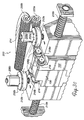
- FIGS. 3F-3I show the details of an exemplary edge roller assembly including two grip rings in accordance with one embodiment of the invention.
- FIG. 3F is a perspective view of this exemplary edge roller assembly.
- edge roller assembly 202 ′′ includes grip rings 222 a ′ and 222 b ′, which are held in an opposing relationship by lower clamp plate 226 and upper clamp plate 228 .
- grip rings 222 a ′ and 222 b ′ are O-rings.
- a plurality of holes 228 a are formed in upper clamp plate 228 .
- Height adjustment knob 208 ′ is mounted on upper clamp plate 228 in the manner explained below with reference to FIG. 3 H.
- FIG. 3G is an exploded view of edge roller assembly 202 ′′ shown in FIG. 3 F.
- lower clamp plate 226 is in the form of a ring having a surface 226 a for receiving grip ring 222 a ′.
- a plurality of holes 226 b are formed in lower clamp plate 226 .
- Upper clamp plate 228 includes a plurality of fingers 228 b - 1 that extend upwardly from an upper surface of the upper clamp plate. Each finger 228 b - 1 has flange 228 b - 2 at the top end thereof so that height adjustment knob 208 ′ can be snapped onto the fingers, as explained in more detail below with reference to FIG. 3 H. As shown in FIG.
- fingers 228 b - 1 form part of a cylinder. This configuration allows height adjustment knob 208 ′ to rotate around fingers 228 b - 1 .
- Upper clamp plate 228 also includes cylindrical portion 228 c that is configured to nest in the central opening of lower clamp plate 226 , as shown in FIG. 3 H.
- FIG. 3H is a cross-sectional view of edge roller assembly 202 ′′ shown in FIG. 3 F.
- holes 226 b in lower clamp plate 226 are provided with recesses configured to receive a screw head.
- Grip ring 222 a ′ is seated against surface 226 a , which is curved so as to conform to the shape of the grip ring.
- Holes 228 a in upper clamp plate 228 are threaded so that lower clamp plate 226 and upper clamp plate 228 can be fastened together with screws or other equivalent fastener.
- the screws fastened in holes 226 b and 228 a are made of Hastelloy; however, it will be apparent to those skilled in the art that the screws may be formed of other suitable materials.
- Grip ring 222 b ′ is seated against surface 228 d , which is curved so as to conform to the shape of the grip ring.
- This clamping force may be controlled by adjusting the torque on the screws that hold lower clamp plate 226 and upper clamp plate 228 together.
- the torque on the screws may be adjusted with a torque wrench or other suitable tool to provide a desired clamping force.
- Height adjustment knob 208 ′ has cylindrical recess 208 a ′ formed therein. Groove 208 b ′ extends around the innermost portion of cylindrical recess 208 a ′. Height adjustment knob 208 ′ may be mounted on upper clamp plate 228 by pushing the height adjustment knob down over fingers 228 b - 1 until flanges 228 b - 2 snap into groove 208 b ′. When fastened to upper clamp plate 228 in this manner, height adjustment knob 208 ′ can be freely rotated around fingers 228 b - 1 , but cannot be moved either up or down because groove 208 b ′ catches flanges 228 b - 2 and thereby prevents axial movement of the height adjustment knob. Those skilled in the art will recognize that other equivalent mechanical fastening techniques may be used to fasten the height adjustment knob to the upper clamp plate.
- Height adjustment knob 208 ′ also has a central threaded hole 208 c ′ formed therein. Threaded hole 208 c ′ is configured to receive the threaded portion of a drive shaft. As shown in FIG. 3H, threaded portion 204 a ′ of drive shaft 204 ′, which extends through central hole 228 e formed in upper clamp plate 228 , is received in threaded hole 208 c ′ of height adjustment knob 208 ′. The height of edge roller assembly 202 ′′ may be adjusted by rotating height adjustment knob 208 ′ so that the height adjustment knob moves up or down on threaded portion 204 a ′ of drive shaft 204 ′.
- central hole 228 e in upper clamp plate 228 conforms to the shape of the remainder of drive shaft 204 ′ so that rotation of the drive shaft will in turn cause rotation of the upper clamp plate and all components connected thereto.
- the remainder of drive shaft 204 ′ i.e., the non-threaded portion of the drive shaft, and central hole 228 e have a rectangular shape.
- these components may have other suitable shapes, e.g., a hexagonal shape.
- FIG. 3I is a simplified schematic diagram that shows a wafer being inserted into the groove defined by two grip rings in accordance with one embodiment of the invention.
- wafer 214 may be moved in the direction indicated by arrow A toward groove G defined by outer surfaces of grip rings 222 a ′ and 222 b ′.
- the curvatures of the outer surfaces of grip rings 222 a ′ and 222 b ′ naturally guide wafer 214 toward the center of groove G. This natural centering action provides more forgiveness in the centering of wafer 214 between grip rings 222 a ′ and 222 b ′.
- the profile of the grip rings may be varied from the O-ring profile shown in FIG. 3 I.
- the grip rings may have a hexagonal profile in the event a more V-shaped groove for receiving the edge of the wafer is desired.
- edge roller assembly 202 ′ may be formed of any suitable material that is capable of withstanding the environment in which the edge roller assembly is to be used.
- the grip rings are standard, commercially available O-rings made of a rubber material.
- Representative rubber materials include VITON rubber (a fluoroelastomer based on the copolymer of vinylidene fluoride and hexafluoropropylene, which is commercially available from Du Pont of Wilmington, Del.), polyurethane rubber, EPDM rubber, and high purity fluoropolymer rubbers, e.g., the fluoropolymer rubbers sold under the trade names KALREZ and CHEMRAZ.
- the rubber material has a Shore A hardness in the range from about 40 to about 90.
- the clamping force exerted on the substrate also may be controlled by varying the hardness of the grip ring material within this range.
- the lower and upper clamp plates and the height adjustment knob are formed of polyethylene terephthalate (PET).
- PET polyethylene terephthalate
- This material is desirable for these components because of its structural rigidity, chemical resistance, lack of particle generation, and lack of outgassing.
- other suitable materials e.g., stainless steel and coated aluminum, may be used to form the clamp plates and the height adjustment knob.
- the diameter of the edge roller assembly is about 2 inches. It will be apparent to those skilled in the art that the diameter of the edge roller assembly may be varied to meet the demands of particular substrates. By way of example, the diameter of the edge roller assembly could be much larger than 2 inches to facilitate the transporting of a larger substrate, e.g., a flat panel display.
- FIG. 4A is a simplified schematic diagram that shows an exemplary configuration of dual radius wheel 108 in accordance with one embodiment of the invention.
- first semicircular section 108 f has radius R 1 and second semicircular section 108 g has radius R 2 , which is shorter than radius R 1 .
- the difference between radius R 1 and radius R 2 is a distance, X, that corresponds to a desired clearance for wafer processing, i.e., the distance between the outer surfaces of O-rings 216 and the backside of wafer 214 when second semicircular section 108 g faces in an upward direction (see FIG. 3 B).
- the transition between first semicircular section 108 f and second semicircular section 108 g occurs at points T.
- the outer surface of each of first semicircular section 108 f and second semicircular section 108 g defines an arc that spans about 180 degrees. Consequently, transition points T are spaced around dual radius wheel 108 by about 180 degrees.
- FIG. 4B is a simplified schematic diagram that shows an exemplary configuration of dual radius wheel 108 ′ in accordance with another embodiment of the invention.
- first semicircular section 108 f has radius R 1 .
- Second semicircular section 108 g has radius R 1 ′, which has the same length as radius R 1 but does not originate at the center of dual radius wheel 108 . Instead, radius R 1 ′ originates at a point that is offset from the center of dual radius wheel 108 by a distance, X, that corresponds to a desired maximum clearance for wafer processing.
- second semicircular section 108 g ′ faces in an upward direction such that points T define a horizontal plane
- the clearance provided by dual radius wheel 108 ′ is the same as that provided by dual radius wheel 108 shown in FIG. 4 A.
- second semicircular section 108 g ′ of dual radius wheel 108 ′ provides a variable clearance.
- the maximum clearance occurs when second semicircular section 108 g ′ faces in an upward direction such that points T define a horizontal plane.
- the clearance decreases as dual radius wheel 108 ′ is rotated away from the point of maximum clearance and reaches a minimum at the point at which points T define a vertical plane. Consequently, the transitions at points T between first semicircular section 108 f and second semicircular section 108 g ′ of dual radius wheel 108 ′ are smoother than the corresponding transitions in dual radius wheel 108 shown in FIG. 4 A.
- FIG. 5 is a flowchart diagram 300 illustrating the method operations performed in transferring a semiconductor wafer from a conveyor system to a wafer processing station in accordance with one embodiment of the invention.
- the method begins in operation 302 in which the wheels of a conveyor system are rotated so that the wafer arrives at a wafer processing station substantially at the level at which the wafer is to be processed in the wafer processing station.
- this may be accomplished by using a conveyor system having a plurality of wheels at least some of which are the dual radius wheels described herein.
- a number of the dual radius wheels of the conveyor system are controllably rotated so that the first sections thereof support the wafer as the wafer arrives at the wafer processing station.
- the wafer processing station is a brush box and the wafer processing operation is a cleaning operation.
- the wafer is clamped with edge clamp devices as the wheels of the conveyor system support the wafer.
- the edge clamp devices are disposed on wafer rotation rollers. To facilitate the edge clamping process, it may be desirable to time the rotation of the wheels so that the wafer arrives at the wafer processing station just past the top height of the wheels. When the wheels are timed in this manner, the wafer may be clamped by the edge clamp devices without having the O-rings disposed on the wheels creating skid marks on the backside of the wafer.
- the method proceeds to operation 306 in which the wheels of the conveyor system are rotated to move the wheels out of contact with the wafer.
- a number of the dual radius wheels of the conveyor system are controllably rotated so that the second sections thereof provide clearance between the dual radius wheels and the wafer.
- the wafer is subjected to a wafer processing operation as the wafer is clamped in the edge clamp devices. Once the wafer processing operation is complete, the method is done.
- a conveyor system of the invention may be provided in the wafer cleaning system between the first and second brush boxes.
- the wafer may be placed at the process position in the first brush box by robotic handoff to edge clamp devices that clamp the edge of the wafer and hold the wafer during processing.
- the wheels of the conveyor system may be controllably rotated to a position at which the wheels clear the wafer.
- the wafer may then be processed in the first brush box.
- the wheels of the conveyor system may be controllably rotated to a position at which the wheels support the wafer.
- the edge clamp devices may then be released so that the wafer rests on the wheels of the conveyor system.
- the wheels of the conveyor system may be rotated to transport the wafer from the first brush box to the second brush box.
- the wafer advances along the conveyor system, the wafer is alternately supported by the first and second sections of the dual radius wheels. Consequently, the wafer tilts up and down in a wave-like manner as it advances along the conveyor system.
- the rotation of the wheels of the conveyor system may be timed so that the wafer is either at or just beyond the peak position of the wafer transport path as the wafer arrives at the second brush box.
- the wafer may then be edge clamped for processing in the second brush box.
- the wheels of the conveyor system may be controllably rotated to a position at which the wheels clear the wafer. To support serial wafer processing at peak efficiency, the action in the second brush box should occur simultaneously with the action in the first brush box.
- the present invention provides an edge roller assembly, a method for contacting an edge of a substrate, and a transport system for transporting semiconductor wafers to a wafer processing station.
- the invention has been described herein in terms of several exemplary embodiments. Other embodiments of the invention will be apparent to those skilled in the art from consideration of the specification and practice of the invention.
- the configuration of the lower clamp plate, the upper clamp plate, and the height adjustment knob of the edge roller assembly may be varied from that shown and described herein.
- other equivalent fastening techniques may be used to join the lower and upper clamp plates and to mount the height adjustment knob on the upper clamp plate.
- the embodiments and preferred features described above should be considered exemplary, with the scope of the invention being defined by the appended claims and their equivalents.
Landscapes
- Container, Conveyance, Adherence, Positioning, Of Wafer (AREA)
- Cleaning Or Drying Semiconductors (AREA)
- Cleaning In General (AREA)
Abstract
An edge roller assembly includes first and second grip rings. The grip rings are held together in an opposing relationship such that outer surfaces thereof define a groove for receiving an edge of a substrate. The grip rings may be O-rings formed of a rubber material. In one embodiment, the grip rings are held together by lower and upper clamp plates that are adjustably fastened together so that the clamping forces exerted on the substrate can be controlled. The upper clamp plate may have a height adjustment knob for adjusting the height of the edge roller assembly mounted thereon. A method for contacting an edge of a substrate and a transport system for transporting semiconductor wafers to a wafer processing station also are described.
Description
This application is a continuation-in-part of Application Ser. No. 09/608,515, filed on Jun. 30, 2000. The disclosure of this application is incorporated herein by reference.
The present invention relates generally to semiconductor fabrication and, more particularly, to an edge roller assembly, a method for contacting an edge of a substrate, and a transport system for transporting semiconductor wafers to a wafer processing station.
In the fabrication of semiconductor devices, a variety of wafer preparation operations are performed. FIG. 1 is a schematic diagram of a conventional wafer cleaning system 50. The cleaning system 50 includes a load station 10 where a plurality of wafers in a cassette 14 may be inserted into the system for cleaning. Once the wafers are inserted into the load station 10, a wafer 12 may be taken from the cassette 14 and moved into a brush station 16, which includes a first brush box 16 a and a second brush box 16 b. The wafer 12 is first moved into first brush box 16 a, where the wafer is scrubbed in a solution containing specified chemicals and deionized (DI) water. The wafer 12 is then moved into second brush box 16 b, where the wafer is again scrubbed in a solution containing specified chemicals and DI water. After the wafer 12 has been scrubbed in brush boxes 16 a and 16 b, the wafer is moved into a spin, rinse, and dry (SRD) station 20 where DI water is sprayed onto the top and bottom surfaces of the wafer as the wafer is spun. After the wafer 12 has been dried, the wafer is moved from SRD station 20 to an unload station 22.
To achieve the best throughput productivity in wafer cleaning system 50, wafer 12 must be rapidly and efficiently transported from first brush box 16 a to second brush box 16 b. In comparison with a conveyor system, a robotic “pick and place” system is a slow and inefficient way to transport a wafer from the first brush box to the second brush box. Conventional conveyor systems, however, suffer from the drawback that they are capable of transporting wafers only in a horizontal plane. Consequently, these conveyor systems do not interface efficiently with the equipment, e.g., edge clamp devices, that handles a wafer during processing because either the wafer or the track must be moved to obtain the clearance required to process the wafer.
Another problem associated with transporting wafers involves the edge clamp devices. One conventional edge clamp device is a one-piece, custom molded roller wheel. This conventional edge clamp device suffers from two primary disadvantages. First, the molded roller wheel is not reliable because the complicated pattern formed therein causes the wheel to fail prematurely. Second, the molded roller wheel is relatively expensive to manufacture and requires a long lead time.
In view of the foregoing, there is a need for a device that efficiently transports a wafer through a wafer processing station such as, for example, a wafer cleaning system having a first brush box and a second brush box. There also is a need for a reliable and cost effective edge clamp device for use in transporting wafers to a wafer processing station.
Broadly speaking, the present invention fills this need by providing an edge roller assembly that reliably grips the edge of a substrate and is simple and cost effective to manufacture. The present invention also provides a method for contacting an edge of a substrate and a transport system for transporting wafers to a wafer processing station.
In accordance with one aspect of the present invention, an edge roller assembly is provided. The edge roller assembly includes a first grip ring and a second grip ring. The first and second grip rings are held together in an opposing relationship such that outer surfaces thereof define a groove for receiving an edge of a substrate, e.g., a wafer.
In one embodiment, the first and second grip rings are O-rings comprised of a rubber material. The rubber material preferably has a Shore A hardness in a range from about 40 to about 90. Representative rubber materials include VITON rubber, polyurethane rubber, EPDM rubber, and fluoropolymer rubber.
In one embodiment, the edge roller assembly includes a lower clamp plate and an upper clamp plate. In this embodiment, the first and second grip rings are disposed between the lower and upper clamp plates in an opposing relationship such that outer surfaces thereof define a groove for receiving an edge of a substrate. The lower and upper clamp plates may be adjustably fastened together so that the clamping forces the lower and upper clamp plates exert on the first and second grip rings can be controlled.
In one embodiment, the lower clamp plate is in the form of a ring having a surface for receiving the first grip ring and a plurality of holes configured to receive a screw head. In one embodiment, the upper clamp plate includes a surface for receiving the second grip ring, a central throughhole for receiving a drive shaft, a plurality of threaded holes, and a plurality of fingers extending from an upper surface thereof. In one embodiment, the edge roller assembly may include a height adjustment knob rotatably disposed on the fingers extending from the upper surface of the upper clamp plate. The height adjustment knob may have a threaded hole formed therein for receiving a threaded portion of the drive shaft. In one embodiment, the lower clamp plate, the upper clamp plate, and the height adjustment knob are formed of polyethylene terephthalate.
In accordance with another aspect of the present invention, a method for contacting an edge of a substrate is provided. In this method a pair of grip rings are clamped together in an opposing relationship such that outer surfaces thereof define a groove. An edge of a substrate, e.g., a wafer, is then inserted into the groove. In one embodiment, the pair of grip rings is clamped together with a controlled force. In one embodiment, the grip rings are O-rings.
In accordance with yet another aspect of the present invention, a transport system for transporting semiconductor wafers to a wafer processing station is provided. This transport system includes a pair of edge roller assemblies disposed in an opposing relationship. Each of the pair of edge roller assemblies includes first and second grip rings, which may be in the form of O-rings, held together in an opposing relationship such that outer surfaces thereof define a groove for receiving an edge of a wafer. In addition, each of the pair of edge roller assemblies is disposed on a rotatable drive shaft. The transport system is well suited to transport wafers to wafer processing stations at which wafer cleaning operations and wafer buffing operations are performed.
The edge roller assembly of the present invention provides a number of significant advantages. First, the edge roller assembly is simple and cost effective to manufacture because it does not require custom molded parts. Second, the configuration of the edge roller assembly enables the clamping forces exerted on the substrate to be controlled. Third, the grip rings are not subject to premature failure because they do not have any complex patterns formed therein. Fourth, the groove for receiving the edge of the substrate defined by the grip rings provides natural centering action. And fifth, the grip rings can be easily changed, which facilitates the use of diverse substrate contact materials to meet the demands of different applications.
It is to be understood that the foregoing general description and the following detailed description are exemplary and explanatory only and are not restrictive of the invention, as claimed.
The accompanying drawings, which are incorporated in and constitute part of this specification, illustrate exemplary embodiments of the invention and together with the description serve to explain the principles of the invention.
FIG. 1 is a schematic diagram of a conventional wafer cleaning system.
FIG. 2A is a simplified perspective view of a conveyor system with dual radius wheels in the “wheels up” position in accordance with one embodiment of the invention.
FIG. 2B is a simplified perspective view of the conveyor system shown in FIG. 2A after the dual radius wheels have been rotated so that they are in the “wheels down” position in accordance with one embodiment of the invention.
FIG. 2C is an enlarged perspective view of a dual radius wheel in accordance with one embodiment of the invention.
FIG. 3A is a simplified elevational view of a wafer processing station including a conveyor system in accordance with one embodiment of the invention.
FIG. 3B is a simplified elevational view of the wafer processing station shown in FIG. 3A after the conveyor system has been moved clear of the wafer for processing in accordance with one embodiment of the invention.
FIG. 3C is a simplified elevational view of the wafer processing station shown in FIG. 3B as the wafer is being subjected to a wafer cleaning operation in accordance with one embodiment of the invention.
FIGS. 3D and 3E show simplified cross-sectional views of two exemplary edge clamp devices that may be used to clamp the edge of the wafer.
FIG. 3F is a perspective view of an exemplary edge roller assembly in accordance with one embodiment of the invention.
FIG. 3G is an exploded view of the edge roller assembly shown in FIG. 3F.
FIG. 3H is a cross-sectional view of the edge roller assembly shown in FIG. 3F.
FIG. 3I is a simplified schematic diagram that shows a wafer being inserted into the groove defined by two grip rings in accordance with one embodiment of the invention.
FIG. 4A is a simplified schematic diagram that shows an exemplary configuration of a dual radius wheel in accordance with one embodiment of the invention.
FIG. 4B is a simplified schematic diagram that shows an exemplary configuration of a dual radius wheel in accordance with another embodiment of the invention.
FIG. 5 is a flowchart diagram illustrating the method operations performed in transferring a semiconductor wafer from a conveyor system to a wafer processing station in accordance with one embodiment of the invention.
Several exemplary embodiments of the invention will now be described in detail with reference to the accompanying drawings. FIG. 1 is discussed above in the “Background of the Invention” section.
FIG. 2A is a simplified perspective view of conveyor system 100 in accordance with one embodiment of the invention. As shown therein, conveyor system 100 includes support stand 102 that has grooves 104 formed in a top surface thereof. Axles 106, which have dual radius wheels 108 mounted on the ends thereof, are disposed in grooves 104. Each of dual radius wheels 108 has inner surface 108 a, outer surface 108 b, and edge surface 108 c, which extends between inner surface 108 a and outer surface 108 b and is configured to receive an O-ring for contacting a semiconductor wafer, as explained in more detail below. Hub 108 d, which has groove 108 e formed therein, is provided on outer surface 108 b. Groove 108 e is configured to receive a timing belt for rotating dual radius wheels 108 in unison.
Each of dual radius wheels 108 has first semicircular section 108 f for supporting a wafer at a first level and second semicircular section 108 g for supporting the wafer at a second level, which is lower than the first level. As shown in FIG. 2A, dual radius wheels 108 are in the “wheels up” position in which first semicircular sections 108 f face in an upward direction. In this position, first semicircular sections 108 f support the wafer at a first level for processing, as described in more detail below. FIG. 2B is a simplified perspective view of conveyor system 100 shown in FIG. 2A after dual radius wheels 108 have been rotated so that they are in the “wheels down” position. As shown in FIG. 2B, second semicircular sections 108 g face in an upward direction. In this position, second semicircular sections 108 g may either support the wafer or provide clearance between the wafer and dual radius wheels 108 during processing, as will be described in more detail later.
FIG. 2C is an enlarged perspective view of a dual radius wheel in accordance with one embodiment of the invention. As shown in FIG. 2C, dual radius wheel 108 includes hub 108 d provided on outer surface 108 b. Hub 108 d has groove 108 e formed therein for receiving a timing belt, as described above. Edge surface 108 c extends between outer surface 108 b and inner surface 108 a (see FIGS. 2A and 2B) and defines a groove for receiving an O-ring that contacts the wafer. Central aperture 109 extends through dual radius wheel 108 and is configured to receive an axle. The transition between first semicircular section 108 f and second semicircular section 108 g occurs at points T (only one of which is visible in FIG. 2C). In one embodiment, each of first semicircular section 108 f and second semicircular section 108 g defines an arc that spans about 180 degrees. Dual radius wheel 108, as well as the other components of the conveyor system, may be formed of well-known materials that are suitable for use in a semiconductor processing environment in which cleaning chemicals are used.
FIG. 3A is a simplified elevational view of a wafer processing station including a conveyor system in accordance with one embodiment of the invention. As shown therein, wafer processing station 200 includes edge roller assemblies 202 a and 202 b, which are mounted on shafts 204 a and 204 b, respectively. Shafts 204 a and 204 b extend into gear housings 206 a and 206 b, respectively, which enclose the drive mechanisms for rotating edge roller assemblies 202 a and 202 b. Height adjustment knobs 208 a and 208 b for adjusting the height of edge roller assemblies 202 a and 202 b, respectively, are provided on shafts 204 a and 204 b, respectively. Lead screws 210 a and 210 b provide lateral movement of gear housings 206 a and 206 b, respectively, so that the lateral position of edge roller assemblies 202 a and 202 b can be adjusted. Edge clamp devices 212 a and 212 b for clamping the edge of semiconductor wafer 214 are disposed on edge roller assemblies 202 a and 202 b, respectively. Additional details of two exemplary edge clamp devices are described below with reference to FIGS. 3D and 3E. Additional details of an exemplary edge roller assembly are described below with reference to FIGS. 3F-3I.
As shown in FIG. 3A, first semicircular sections 108 f of dual radius wheels 108 (see, e.g., FIGS. 2A and 2B) of conveyor system 100 support wafer 214 at the level at which the wafer will be processed in wafer processing station 200. More particularly, O-rings 216, which are disposed in edge surface 108 c (see, e.g., FIG. 2C) of each dual radius wheel 108, contact the backside of wafer 214 and thereby support the wafer. As shown in FIG. 3A, conveyor system 100 includes three pairs of dual radius wheels 108, with each pair of wheels being arranged in an opposing relationship on opposite sides of support stand 102. Timing belt 218 a rotates the set of dual radius wheels 108 situated on the left side of support stand 102 and timing belt 218 b rotates the set of wheels situated on the right side of the support stand. Timing belts 218 a and 218 b are disposed in grooves 108 e formed in hubs 108 d, as shown, for example, in FIG. 2A.
FIG. 3B is a simplified elevational view of wafer processing station 200 shown in FIG. 3A after conveyor system 100 has been moved clear of wafer 214 for processing in accordance with one embodiment of the invention. As shown in FIG. 3B, dual radius wheels 108 have been rotated so that second semicircular sections 108 g face in an upward direction toward the backside of wafer 214. Second semicircular section 108 g is configured to provide sufficient clearance for safely processing wafer 214. Consequently, when second semicircular sections 108 g are positioned as shown in FIG. 3B, a gap is defined between the outer surfaces of O-rings 216 disposed on dual radius wheels 108 and the backside of wafer 214. In one embodiment, second semicircular section 108 g is configured such that the gap, i.e., the distance between the outer surfaces of O-rings 216 and the backside of wafer 214, is in the range from about one sixteenth ({fraction (1/16)}) of an inch to about three sixteenths ({fraction (3/16)}) of an inch, with the range from about one eighth (⅛) of an inch to about three sixteenths ({fraction (3/16)}) of an inch being preferred. The configuration of second semicircular section 108 g is discussed in more detail below with reference to FIGS. 4A and 4B.
It will be apparent to those skilled in the art that the center-to-center spacing of dual radius wheels 108 of conveyor system 100 must be selected to ensure that wafer 214 is adequately supported as the wafer advances along the conveyor system. Generally speaking, for 8-inch wafers, the center-to-center spacing should not exceed about 3.6 inches. For 12-inch wafers, the center-to-center spacing should not exceed about 5.5 inches.
FIG. 3C is a simplified elevational view of wafer processing station 200 shown in FIG. 3B as wafer 214 is being subjected to a wafer cleaning operation in accordance with one embodiment of the invention. As shown in FIG. 3C, wafer processing station 200 is a brush box in which wafer 214 is being cleaned by rotating brushes 220 a and 220 b. The arrows in FIG. 3C indicate the respective directions in which lower brush 220 a and upper brush 220 b rotate during cleaning. With dual radius wheels 108 of conveyor system 100 rotated out of contact with wafer 214 as described above in connection with FIG. 3B, the wafer is otherwise supported in the process plane for the cleaning operation. In particular, edge clamp devices 212 a and 212 b, which are disposed on edge roller assemblies 202 a and 202 b, respectively, and lower brush 220 a support wafer 214 in the process plane for cleaning.
FIGS. 3D and 3E show simplified cross-sectional views of two exemplary edge clamp devices that may be used to clamp the edge of the wafer. FIG. 3D shows a double O-ring edge clamp device including O- rings 222 a and 222 b disposed around edge roller assembly 202. FIG. 3E shows a polyurethane pad edge clamp device in which polyurethane pad 224 is supported in a V-shaped groove defined in edge roller assembly 202′.
FIGS. 3F-3I show the details of an exemplary edge roller assembly including two grip rings in accordance with one embodiment of the invention. FIG. 3F is a perspective view of this exemplary edge roller assembly. As shown in FIG. 3F, edge roller assembly 202″ includes grip rings 222 a′ and 222 b′, which are held in an opposing relationship by lower clamp plate 226 and upper clamp plate 228. In one embodiment, grip rings 222 a′ and 222 b′ are O-rings. A plurality of holes 228 a, the purpose of which will be explained later, are formed in upper clamp plate 228. Height adjustment knob 208′ is mounted on upper clamp plate 228 in the manner explained below with reference to FIG. 3H.
FIG. 3G is an exploded view of edge roller assembly 202″ shown in FIG. 3F. As shown in FIG. 3G, lower clamp plate 226 is in the form of a ring having a surface 226 a for receiving grip ring 222 a′. A plurality of holes 226 b, the purpose of which will be explained later, are formed in lower clamp plate 226. Upper clamp plate 228 includes a plurality of fingers 228 b-1 that extend upwardly from an upper surface of the upper clamp plate. Each finger 228 b-1 has flange 228 b-2 at the top end thereof so that height adjustment knob 208′ can be snapped onto the fingers, as explained in more detail below with reference to FIG. 3H. As shown in FIG. 3G, fingers 228 b-1 form part of a cylinder. This configuration allows height adjustment knob 208′ to rotate around fingers 228 b-1. Upper clamp plate 228 also includes cylindrical portion 228 c that is configured to nest in the central opening of lower clamp plate 226, as shown in FIG. 3H.
FIG. 3H is a cross-sectional view of edge roller assembly 202″ shown in FIG. 3F. As shown in FIG. 3H, holes 226 b in lower clamp plate 226 are provided with recesses configured to receive a screw head. Grip ring 222 a′ is seated against surface 226 a, which is curved so as to conform to the shape of the grip ring. Holes 228 a in upper clamp plate 228 are threaded so that lower clamp plate 226 and upper clamp plate 228 can be fastened together with screws or other equivalent fastener. In one embodiment, the screws fastened in holes 226 b and 228 a are made of Hastelloy; however, it will be apparent to those skilled in the art that the screws may be formed of other suitable materials. Grip ring 222 b′ is seated against surface 228 d, which is curved so as to conform to the shape of the grip ring. The overlap between grip ring 222 a′ and grip ring 222 b′, which is indicated by the darkened Section X in FIG. 3H, represents the clamping force that lower clamp plate 226 and upper clamp plate 228 exert on the grip rings. This clamping force may be controlled by adjusting the torque on the screws that hold lower clamp plate 226 and upper clamp plate 228 together. The torque on the screws may be adjusted with a torque wrench or other suitable tool to provide a desired clamping force.
FIG. 3I is a simplified schematic diagram that shows a wafer being inserted into the groove defined by two grip rings in accordance with one embodiment of the invention. As shown in FIG. 3I, wafer 214 may be moved in the direction indicated by arrow A toward groove G defined by outer surfaces of grip rings 222 a′ and 222 b′. The curvatures of the outer surfaces of grip rings 222 a′ and 222 b′ naturally guide wafer 214 toward the center of groove G. This natural centering action provides more forgiveness in the centering of wafer 214 between grip rings 222 a′ and 222 b′. If desired, the profile of the grip rings may be varied from the O-ring profile shown in FIG. 3I. By way of example, the grip rings may have a hexagonal profile in the event a more V-shaped groove for receiving the edge of the wafer is desired.
The components of edge roller assembly 202′ may be formed of any suitable material that is capable of withstanding the environment in which the edge roller assembly is to be used. In one embodiment, the grip rings are standard, commercially available O-rings made of a rubber material. Representative rubber materials include VITON rubber (a fluoroelastomer based on the copolymer of vinylidene fluoride and hexafluoropropylene, which is commercially available from Du Pont of Wilmington, Del.), polyurethane rubber, EPDM rubber, and high purity fluoropolymer rubbers, e.g., the fluoropolymer rubbers sold under the trade names KALREZ and CHEMRAZ. In one embodiment, the rubber material has a Shore A hardness in the range from about 40 to about 90. In addition to adjusting the torque on the screws that hold the lower and upper clamp plates together, the clamping force exerted on the substrate also may be controlled by varying the hardness of the grip ring material within this range. Those skilled in the art will recognize that one significant advantage of the present invention is that it facilitates the use of diverse substrate contact materials. In the event a different substrate contact material is needed, the grip rings mounted on the edge roller assembly may be easily replaced with grip rings made of the desired material.
In one embodiment, the lower and upper clamp plates and the height adjustment knob are formed of polyethylene terephthalate (PET). This material is desirable for these components because of its structural rigidity, chemical resistance, lack of particle generation, and lack of outgassing. In environments that do not require one or more of these characteristics, other suitable materials, e.g., stainless steel and coated aluminum, may be used to form the clamp plates and the height adjustment knob. In one embodiment designed to transport 300 mm wafers, the diameter of the edge roller assembly is about 2 inches. It will be apparent to those skilled in the art that the diameter of the edge roller assembly may be varied to meet the demands of particular substrates. By way of example, the diameter of the edge roller assembly could be much larger than 2 inches to facilitate the transporting of a larger substrate, e.g., a flat panel display.
FIG. 4A is a simplified schematic diagram that shows an exemplary configuration of dual radius wheel 108 in accordance with one embodiment of the invention. As shown in FIG. 4A, first semicircular section 108 f has radius R1 and second semicircular section 108 g has radius R2, which is shorter than radius R1. The difference between radius R1 and radius R2 is a distance, X, that corresponds to a desired clearance for wafer processing, i.e., the distance between the outer surfaces of O-rings 216 and the backside of wafer 214 when second semicircular section 108 g faces in an upward direction (see FIG. 3B). The transition between first semicircular section 108 f and second semicircular section 108 g occurs at points T. In this exemplary configuration, the outer surface of each of first semicircular section 108 f and second semicircular section 108 g defines an arc that spans about 180 degrees. Consequently, transition points T are spaced around dual radius wheel 108 by about 180 degrees.
FIG. 4B is a simplified schematic diagram that shows an exemplary configuration of dual radius wheel 108′ in accordance with another embodiment of the invention. As shown in FIG. 4B, first semicircular section 108 f has radius R1. Second semicircular section 108 g has radius R1′, which has the same length as radius R1 but does not originate at the center of dual radius wheel 108. Instead, radius R1′ originates at a point that is offset from the center of dual radius wheel 108 by a distance, X, that corresponds to a desired maximum clearance for wafer processing. When second semicircular section 108 g′ faces in an upward direction such that points T define a horizontal plane, the clearance provided by dual radius wheel 108′ is the same as that provided by dual radius wheel 108 shown in FIG. 4A. In contrast with the constant clearance provided by second semicircular section 108 g of dual radius wheel 108, second semicircular section 108 g′ of dual radius wheel 108′ provides a variable clearance. The maximum clearance occurs when second semicircular section 108 g′ faces in an upward direction such that points T define a horizontal plane. The clearance decreases as dual radius wheel 108′ is rotated away from the point of maximum clearance and reaches a minimum at the point at which points T define a vertical plane. Consequently, the transitions at points T between first semicircular section 108 f and second semicircular section 108 g′ of dual radius wheel 108′ are smoother than the corresponding transitions in dual radius wheel 108 shown in FIG. 4A.
FIG. 5 is a flowchart diagram 300 illustrating the method operations performed in transferring a semiconductor wafer from a conveyor system to a wafer processing station in accordance with one embodiment of the invention. The method begins in operation 302 in which the wheels of a conveyor system are rotated so that the wafer arrives at a wafer processing station substantially at the level at which the wafer is to be processed in the wafer processing station. By way of example, this may be accomplished by using a conveyor system having a plurality of wheels at least some of which are the dual radius wheels described herein. In one embodiment, a number of the dual radius wheels of the conveyor system are controllably rotated so that the first sections thereof support the wafer as the wafer arrives at the wafer processing station. In one embodiment, the wafer processing station is a brush box and the wafer processing operation is a cleaning operation.
In operation 304, the wafer is clamped with edge clamp devices as the wheels of the conveyor system support the wafer. In one embodiment, the edge clamp devices are disposed on wafer rotation rollers. To facilitate the edge clamping process, it may be desirable to time the rotation of the wheels so that the wafer arrives at the wafer processing station just past the top height of the wheels. When the wheels are timed in this manner, the wafer may be clamped by the edge clamp devices without having the O-rings disposed on the wheels creating skid marks on the backside of the wafer. Once the wafer is edge clamped, the method proceeds to operation 306 in which the wheels of the conveyor system are rotated to move the wheels out of contact with the wafer. In one embodiment, a number of the dual radius wheels of the conveyor system are controllably rotated so that the second sections thereof provide clearance between the dual radius wheels and the wafer. After the wheels have been moved clear of the wafer, in operation 308, the wafer is subjected to a wafer processing operation as the wafer is clamped in the edge clamp devices. Once the wafer processing operation is complete, the method is done.
The wheel, conveyor system, and method described herein are well suited for transporting a wafer in a wafer cleaning system from a first brush box to a second brush box. By way of example, a conveyor system of the invention may be provided in the wafer cleaning system between the first and second brush boxes. At the outset, the wafer may be placed at the process position in the first brush box by robotic handoff to edge clamp devices that clamp the edge of the wafer and hold the wafer during processing. Before the wafer is processed in the first brush box, the wheels of the conveyor system may be controllably rotated to a position at which the wheels clear the wafer. The wafer may then be processed in the first brush box. Once this processing is complete, the wheels of the conveyor system may be controllably rotated to a position at which the wheels support the wafer. The edge clamp devices may then be released so that the wafer rests on the wheels of the conveyor system.
At this point, the wheels of the conveyor system may be rotated to transport the wafer from the first brush box to the second brush box. As the wafer advances along the conveyor system, the wafer is alternately supported by the first and second sections of the dual radius wheels. Consequently, the wafer tilts up and down in a wave-like manner as it advances along the conveyor system. The rotation of the wheels of the conveyor system may be timed so that the wafer is either at or just beyond the peak position of the wafer transport path as the wafer arrives at the second brush box. The wafer may then be edge clamped for processing in the second brush box. Before the wafer is processed in the second brush box, the wheels of the conveyor system may be controllably rotated to a position at which the wheels clear the wafer. To support serial wafer processing at peak efficiency, the action in the second brush box should occur simultaneously with the action in the first brush box.
In summary, the present invention provides an edge roller assembly, a method for contacting an edge of a substrate, and a transport system for transporting semiconductor wafers to a wafer processing station. The invention has been described herein in terms of several exemplary embodiments. Other embodiments of the invention will be apparent to those skilled in the art from consideration of the specification and practice of the invention. For example, the configuration of the lower clamp plate, the upper clamp plate, and the height adjustment knob of the edge roller assembly may be varied from that shown and described herein. In addition, other equivalent fastening techniques may be used to join the lower and upper clamp plates and to mount the height adjustment knob on the upper clamp plate. The embodiments and preferred features described above should be considered exemplary, with the scope of the invention being defined by the appended claims and their equivalents.
Claims (14)
1. An edge roller assembly, comprising:
a lower clamp plate;
an upper clamp plate having a receiving surface, a central throughhole for receiving a drive shaft, a plurality of threaded holes, and a plurality of fingers, the plurality of fingers extending from an upper surface of the upper clamp plate;
a first grip ring; and
a second grip ring seated against the receiving surface of the upper clamp plate, the first and second grip rings being disposed between the lower and upper clamp plates in an opposing relationship such that outer surfaces thereof define a groove for receiving an edge of a substrate, and the lower and upper clamp plates being adjustably fastened together so that clamping forces the lower and upper clamp plates exert on the first and second grip rings can be controlled.
2. The edge roller assembly of claim 1 , wherein the lower clamp plate is a ring having a surface for receiving the first grip ring and a plurality of holes configured to receive a screw head.
3. The edge roller assembly of claim 1 , further comprising:
a height adjustment knob rotatably disposed on the plurality of fingers extending from the upper surface of the upper clamp plate, the height adjustment knob having a threaded hole formed therein for receiving a threaded portion of the drive shaft.
4. The edge roller assembly of claim 1 , wherein the first and second grip rings are O-rings comprised of a rubber material.
5. The edge roller assembly of claim 4 , wherein the rubber material has a Shore A hardness in a range from about 40 to about 90.
6. The edge roller assembly of claim 5 , wherein the rubber material is selected from the group consisting of VITON rubber, polyurethane rubber, EPDM rubber, and fluoropolymer rubber.
7. The edge roller assembly of claim 3 , wherein the lower clamp plate, the upper clamp plate, and the height adjustment knob are comprised of polyethylene terephthalate.
8. A transport system for transporting semiconductor wafers to a wafer processing station, comprising:
a pair of edge roller assemblies disposed in an opposing relationship, each of the pair of edge roller assemblies being disposed on a rotatable drive shaft, and each of the pair of edge roller assemblies including
a lower clamp plate;
an upper clamp plate having a receiving surface, a central throughhole for receiving the rotatable drive shaft, a plurality of threaded holes, and a plurality of fingers, the plurality of fingers extending from an upper surface of the upper clamp plate;
a first grip ring; and
a second grip ring seated against the receiving surface of the upper clamp plate, the first and second grip rings being disposed between the lower and upper clamp plates in an opposing relationship such that outer surfaces thereof define a groove for receiving an edge of a substrate, and the lower and upper clamp plates being adjustably fastened together so that clamping forces the lower and upper clamp plates exert on the first and second grip rings can be controlled.
9. The transport system of claim 8 , wherein the lower clamp plate in each of the pair of edge roller assemblies is a ring having a surface for receiving the first grip ring and a plurality of holes configured to receive a screw head.
10. The transport system of claim 8 , wherein each of the pair of edge roller assemblies further comprises:
a height adjustment knob rotatably disposed on the plurality of fingers extending from the upper surface of the upper clamp plate, the height adjustment knob having a threaded hole formed therein for receiving a threaded portion of the rotatable drive shaft.
11. The transport system of claim 8 , wherein the first and second grip rings in each of the pair of edge roller assemblies are O-rings comprised of a rubber material.
12. The transport system of claim 11 , wherein the rubber material has a Shore A hardness in a range from about 40 to about 90.
13. The transport system of claim 12 , wherein the rubber material is selected from the group consisting of VITON rubber, polyurethane rubber, EPDM rubber, and fluoropolymer rubber.
14. The transport system of claim 10 , wherein the lower clamp plate, the upper clamp plate, and the height adjustment knob in each of the pair of edge roller assemblies are comprised of polyethylene terephthalate.
Priority Applications (1)
| Application Number | Priority Date | Filing Date | Title |
|---|---|---|---|
| US09/687,747 US6752162B1 (en) | 2000-06-30 | 2000-10-13 | Edge roller assembly, method for contacting an edge of a substrate, and transport system for transporting semiconductor wafers to a wafer processing station |
Applications Claiming Priority (2)
| Application Number | Priority Date | Filing Date | Title |
|---|---|---|---|
| US09/608,515 US6439245B1 (en) | 2000-06-30 | 2000-06-30 | Method for transferring wafers from a conveyor system to a wafer processing station |
| US09/687,747 US6752162B1 (en) | 2000-06-30 | 2000-10-13 | Edge roller assembly, method for contacting an edge of a substrate, and transport system for transporting semiconductor wafers to a wafer processing station |
Related Parent Applications (1)
| Application Number | Title | Priority Date | Filing Date |
|---|---|---|---|
| US09/608,515 Continuation-In-Part US6439245B1 (en) | 2000-06-30 | 2000-06-30 | Method for transferring wafers from a conveyor system to a wafer processing station |
Publications (1)
| Publication Number | Publication Date |
|---|---|
| US6752162B1 true US6752162B1 (en) | 2004-06-22 |
Family
ID=24436838
Family Applications (3)
| Application Number | Title | Priority Date | Filing Date |
|---|---|---|---|
| US09/608,515 Expired - Lifetime US6439245B1 (en) | 2000-06-30 | 2000-06-30 | Method for transferring wafers from a conveyor system to a wafer processing station |
| US09/687,747 Expired - Fee Related US6752162B1 (en) | 2000-06-30 | 2000-10-13 | Edge roller assembly, method for contacting an edge of a substrate, and transport system for transporting semiconductor wafers to a wafer processing station |
| US10/193,803 Expired - Lifetime US6607072B2 (en) | 2000-06-30 | 2002-07-11 | Wheel and conveyor system for transporting semiconductor wafers |
Family Applications Before (1)
| Application Number | Title | Priority Date | Filing Date |
|---|---|---|---|
| US09/608,515 Expired - Lifetime US6439245B1 (en) | 2000-06-30 | 2000-06-30 | Method for transferring wafers from a conveyor system to a wafer processing station |
Family Applications After (1)
| Application Number | Title | Priority Date | Filing Date |
|---|---|---|---|
| US10/193,803 Expired - Lifetime US6607072B2 (en) | 2000-06-30 | 2002-07-11 | Wheel and conveyor system for transporting semiconductor wafers |
Country Status (4)
| Country | Link |
|---|---|
| US (3) | US6439245B1 (en) |
| AU (1) | AU2001273658A1 (en) |
| TW (1) | TW492064B (en) |
| WO (1) | WO2002003433A2 (en) |
Cited By (5)
| Publication number | Priority date | Publication date | Assignee | Title |
|---|---|---|---|---|
| US7056392B1 (en) * | 2003-04-16 | 2006-06-06 | Lsi Logic Corporation | Wafer chucking apparatus and method for spin processor |
| US20090217953A1 (en) * | 2008-02-28 | 2009-09-03 | Hui Chen | Drive roller for a cleaning system |
| CN102815525A (en) * | 2012-07-18 | 2012-12-12 | 苏州汾湖电梯有限公司 | Guiding and locating device |
| US20210114832A1 (en) * | 2018-06-14 | 2021-04-22 | Applied Materials, Inc. | Roller device for guiding a flexible substrate, use of a roller device for transporting a flexible substrate, vacuum processing apparatus, and method of processing a flexible substrate |
| WO2025264447A1 (en) * | 2024-06-21 | 2025-12-26 | Applied Materials, Inc. | Chemical mechanical polisher cleaning unit |
Families Citing this family (13)
| Publication number | Priority date | Publication date | Assignee | Title |
|---|---|---|---|---|
| US6918864B1 (en) * | 1999-06-01 | 2005-07-19 | Applied Materials, Inc. | Roller that avoids substrate slippage |
| US6622334B1 (en) * | 2000-03-29 | 2003-09-23 | International Business Machines Corporation | Wafer edge cleaning utilizing polish pad material |
| US6439245B1 (en) * | 2000-06-30 | 2002-08-27 | Lam Research Corporation | Method for transferring wafers from a conveyor system to a wafer processing station |
| JP2002052370A (en) * | 2000-08-09 | 2002-02-19 | Ebara Corp | Substrate cleaning device |
| US7067016B1 (en) * | 2003-03-31 | 2006-06-27 | Lam Research Corporation | Chemically assisted mechanical cleaning of MRAM structures |
| US20050109371A1 (en) * | 2003-10-27 | 2005-05-26 | Applied Materials, Inc. | Post CMP scrubbing of substrates |
| EP1635223A3 (en) * | 2004-08-27 | 2009-11-11 | FUJIFILM Corporation | Processing apparatus for lithographic printing plate and process for processing the same |
| TW200809936A (en) * | 2006-06-05 | 2008-02-16 | Applied Materials Inc | Methods and apparatus for supporting a substrate in a horizontal orientation during cleaning |
| US7780825B2 (en) * | 2007-05-21 | 2010-08-24 | Lam Research Corporation | Substrate gripper with integrated electrical contacts |
| CN101958402B (en) * | 2010-05-25 | 2012-02-29 | 东莞宏威数码机械有限公司 | Tightness-adjustable substrate transmission device |
| JP7348021B2 (en) * | 2019-10-15 | 2023-09-20 | 株式会社荏原製作所 | Substrate cleaning equipment and substrate cleaning method |
| CN113394140B (en) * | 2021-07-02 | 2024-07-23 | 北京北方华创微电子装备有限公司 | Semiconductor cleaning equipment and its robot |
| CN117316862B (en) * | 2023-10-23 | 2024-04-05 | 昆山日月同芯半导体有限公司 | Wafer clamping mechanism and wafer transmission equipment |
Citations (10)
| Publication number | Priority date | Publication date | Assignee | Title |
|---|---|---|---|---|
| US4217977A (en) | 1978-09-15 | 1980-08-19 | The Silicon Valley Group, Inc. | Conveyor system |
| US4313266A (en) | 1980-05-01 | 1982-02-02 | The Silicon Valley Group, Inc. | Method and apparatus for drying wafers |
| US5839460A (en) * | 1997-11-13 | 1998-11-24 | Memc Electronic Materials, Inc. | Apparatus for cleaning semiconductor wafers |
| US5840129A (en) * | 1994-07-15 | 1998-11-24 | Ontrak Systems, Inc. | Hesitation free roller |
| US5862560A (en) * | 1996-08-29 | 1999-01-26 | Ontrak Systems, Inc. | Roller with treading and system including the same |
| WO1999004416A1 (en) | 1997-07-17 | 1999-01-28 | Kunze Concewitz Horst | Method and device for treating two-dimensional substrates, especially silicon slices (wafers), for producing microelectronic components |
| US5924154A (en) | 1996-08-29 | 1999-07-20 | Ontrak Systems, Inc. | Brush assembly apparatus |
| US6021791A (en) | 1998-06-29 | 2000-02-08 | Speedfam-Ipec Corporation | Method and apparatus for immersion cleaning of semiconductor devices |
| EP1058296A2 (en) * | 1999-06-01 | 2000-12-06 | Applied Materials, Inc. | A roller for rotating a substrate |
| US6439245B1 (en) * | 2000-06-30 | 2002-08-27 | Lam Research Corporation | Method for transferring wafers from a conveyor system to a wafer processing station |
Family Cites Families (20)
| Publication number | Priority date | Publication date | Assignee | Title |
|---|---|---|---|---|
| GB365441A (en) * | 1930-05-03 | 1932-01-21 | Muller J C & Co | Apparatus for delivering cigarettes from a continuous rod cigarette-making machine |
| US2580469A (en) * | 1950-06-01 | 1952-01-01 | Johnson & Johnson | Cam device for varying speed of an object |
| FR2102423A5 (en) * | 1970-08-03 | 1972-04-07 | Decoufle Usines | |
| SU470159A1 (en) * | 1971-12-22 | 1976-08-25 | Издательство "Известия" Советов Депутатов Трудящихся Ссср | Device for moving piece goods in two mutually perpendicular directions |
| US4181214A (en) * | 1977-11-25 | 1980-01-01 | Kasper Instruments, Inc. | Wafer transfer apparatus |
| US4505381A (en) * | 1983-05-23 | 1985-03-19 | Harry Major Machine And Tool Co. | Conveyor roller |
| US4846623A (en) * | 1986-10-08 | 1989-07-11 | Dainippon Screen Mfg. Co., Ltd. | Wafer transferring device |
| US5176158A (en) * | 1991-10-29 | 1993-01-05 | Chemcut Corporation | Apparatus and method for transporting materials which are to be chemically treated |
| US5345639A (en) * | 1992-05-28 | 1994-09-13 | Tokyo Electron Limited | Device and method for scrubbing and cleaning substrate |
| JP2888412B2 (en) * | 1994-07-04 | 1999-05-10 | 信越半導体株式会社 | Brush cleaning device and work cleaning system |
| US5795405A (en) * | 1996-03-13 | 1998-08-18 | Eric F. Harnden | Machine and method for processing of printed circuit boards by immersion in transversely flowing liquid chemical |
| US5810549A (en) * | 1996-04-17 | 1998-09-22 | Applied Materials, Inc. | Independent linear dual-blade robot and method for transferring wafers |
| US5899216A (en) * | 1996-07-08 | 1999-05-04 | Speedfam Corporation | Apparatus for rinsing wafers in the context of a combined cleaning rinsing and drying system |
| US5789878A (en) * | 1996-07-15 | 1998-08-04 | Applied Materials, Inc. | Dual plane robot |
| DE69737926T2 (en) * | 1996-10-21 | 2008-04-10 | Ebara Corp. | cleaning device |
| AT406041B (en) * | 1997-01-29 | 2000-01-25 | Knapp Holding Gmbh | SWITCH FOR A CONVEYOR |
| JP3850951B2 (en) * | 1997-05-15 | 2006-11-29 | 東京エレクトロン株式会社 | Substrate transport apparatus and substrate transport method |
| JPH10314684A (en) * | 1997-05-21 | 1998-12-02 | Speedfam Co Ltd | Cleaning method and apparatus for disk-shaped workpiece |
| JP3331168B2 (en) * | 1997-12-09 | 2002-10-07 | ティーディーケイ株式会社 | Cleaning method and apparatus |
| US6217272B1 (en) * | 1998-10-01 | 2001-04-17 | Applied Science And Technology, Inc. | In-line sputter deposition system |
-
2000
- 2000-06-30 US US09/608,515 patent/US6439245B1/en not_active Expired - Lifetime
- 2000-10-13 US US09/687,747 patent/US6752162B1/en not_active Expired - Fee Related
-
2001
- 2001-06-29 AU AU2001273658A patent/AU2001273658A1/en not_active Abandoned
- 2001-06-29 WO PCT/US2001/041219 patent/WO2002003433A2/en not_active Ceased
- 2001-06-29 TW TW090116299A patent/TW492064B/en not_active IP Right Cessation
-
2002
- 2002-07-11 US US10/193,803 patent/US6607072B2/en not_active Expired - Lifetime
Patent Citations (10)
| Publication number | Priority date | Publication date | Assignee | Title |
|---|---|---|---|---|
| US4217977A (en) | 1978-09-15 | 1980-08-19 | The Silicon Valley Group, Inc. | Conveyor system |
| US4313266A (en) | 1980-05-01 | 1982-02-02 | The Silicon Valley Group, Inc. | Method and apparatus for drying wafers |
| US5840129A (en) * | 1994-07-15 | 1998-11-24 | Ontrak Systems, Inc. | Hesitation free roller |
| US5862560A (en) * | 1996-08-29 | 1999-01-26 | Ontrak Systems, Inc. | Roller with treading and system including the same |
| US5924154A (en) | 1996-08-29 | 1999-07-20 | Ontrak Systems, Inc. | Brush assembly apparatus |
| WO1999004416A1 (en) | 1997-07-17 | 1999-01-28 | Kunze Concewitz Horst | Method and device for treating two-dimensional substrates, especially silicon slices (wafers), for producing microelectronic components |
| US5839460A (en) * | 1997-11-13 | 1998-11-24 | Memc Electronic Materials, Inc. | Apparatus for cleaning semiconductor wafers |
| US6021791A (en) | 1998-06-29 | 2000-02-08 | Speedfam-Ipec Corporation | Method and apparatus for immersion cleaning of semiconductor devices |
| EP1058296A2 (en) * | 1999-06-01 | 2000-12-06 | Applied Materials, Inc. | A roller for rotating a substrate |
| US6439245B1 (en) * | 2000-06-30 | 2002-08-27 | Lam Research Corporation | Method for transferring wafers from a conveyor system to a wafer processing station |
Cited By (5)
| Publication number | Priority date | Publication date | Assignee | Title |
|---|---|---|---|---|
| US7056392B1 (en) * | 2003-04-16 | 2006-06-06 | Lsi Logic Corporation | Wafer chucking apparatus and method for spin processor |
| US20090217953A1 (en) * | 2008-02-28 | 2009-09-03 | Hui Chen | Drive roller for a cleaning system |
| CN102815525A (en) * | 2012-07-18 | 2012-12-12 | 苏州汾湖电梯有限公司 | Guiding and locating device |
| US20210114832A1 (en) * | 2018-06-14 | 2021-04-22 | Applied Materials, Inc. | Roller device for guiding a flexible substrate, use of a roller device for transporting a flexible substrate, vacuum processing apparatus, and method of processing a flexible substrate |
| WO2025264447A1 (en) * | 2024-06-21 | 2025-12-26 | Applied Materials, Inc. | Chemical mechanical polisher cleaning unit |
Also Published As
| Publication number | Publication date |
|---|---|
| US20020174881A1 (en) | 2002-11-28 |
| US6439245B1 (en) | 2002-08-27 |
| AU2001273658A1 (en) | 2002-01-14 |
| TW492064B (en) | 2002-06-21 |
| WO2002003433A3 (en) | 2002-08-15 |
| US6607072B2 (en) | 2003-08-19 |
| WO2002003433A2 (en) | 2002-01-10 |
Similar Documents
| Publication | Publication Date | Title |
|---|---|---|
| US6752162B1 (en) | Edge roller assembly, method for contacting an edge of a substrate, and transport system for transporting semiconductor wafers to a wafer processing station | |
| US6012192A (en) | Substrate processing apparatus | |
| TWI464829B (en) | Grounded chuck | |
| US6059889A (en) | Method for processing a substrate using a system having a roller with treading | |
| CN1722373B (en) | Substrate meniscus interface and methods for operation | |
| TWI728703B (en) | Spin chuck of substrate processing apparatus | |
| US6003185A (en) | Hesitation free roller | |
| US7743449B2 (en) | System and method for a combined contact and non-contact wafer cleaning module | |
| JP6073192B2 (en) | Substrate cleaning apparatus, substrate cleaning system, and substrate cleaning method | |
| US6964419B2 (en) | Chuck rollers and pins for substrate cleaning and drying system | |
| JP3291108B2 (en) | Substrate processing method and apparatus | |
| US7007333B1 (en) | System and method for a combined contact and non-contact wafer cleaning module | |
| JP3513378B2 (en) | Substrate processing equipment | |
| US5893568A (en) | Substrate support device | |
| US20090217953A1 (en) | Drive roller for a cleaning system | |
| US6039187A (en) | Off center three point carrier for wet processing semiconductor substrates | |
| KR20090051521A (en) | Substrate conveying blade and substrate conveying apparatus having same | |
| KR20210116988A (en) | Transporting blade and substrate transporting device, substrate treatment system | |
| KR100583942B1 (en) | Fixing Device for Wafer for Double Sided Processing | |
| US11940724B2 (en) | Reticle processing system | |
| US12538752B2 (en) | Apparatus for processing a wafer-shaped article | |
| KR100828422B1 (en) | Substrate Transfer Device | |
| JPH0377347A (en) | Method for aligning facet of wafer | |
| KR100316606B1 (en) | Handler for semiconductor wafer | |
| KR100793385B1 (en) | Board Alignment Device |
Legal Events
| Date | Code | Title | Description |
|---|---|---|---|
| AS | Assignment |
Owner name: LAM RESEARCH CORPORATION, CALIFORNIA Free format text: ASSIGNMENT OF ASSIGNORS INTEREST;ASSIGNORS:GARDNER, DOUGLAS G.;SMITH, STEPHEN MARK;BLIVEN, BRIAN M.;REEL/FRAME:011265/0090 Effective date: 20001013 |
|
| FPAY | Fee payment |
Year of fee payment: 4 |
|
| REMI | Maintenance fee reminder mailed | ||
| FPAY | Fee payment |
Year of fee payment: 8 |
|
| REMI | Maintenance fee reminder mailed | ||
| LAPS | Lapse for failure to pay maintenance fees | ||
| STCH | Information on status: patent discontinuation |
Free format text: PATENT EXPIRED DUE TO NONPAYMENT OF MAINTENANCE FEES UNDER 37 CFR 1.362 |
|
| FP | Lapsed due to failure to pay maintenance fee |
Effective date: 20160622 |