US6646579B2 - Method and device for generating OVSF code words - Google Patents
Method and device for generating OVSF code words Download PDFInfo
- Publication number
- US6646579B2 US6646579B2 US10/203,067 US20306702A US6646579B2 US 6646579 B2 US6646579 B2 US 6646579B2 US 20306702 A US20306702 A US 20306702A US 6646579 B2 US6646579 B2 US 6646579B2
- Authority
- US
- United States
- Prior art keywords
- code
- word
- calculation
- ovsf
- code word
- Prior art date
- Legal status (The legal status is an assumption and is not a legal conclusion. Google has not performed a legal analysis and makes no representation as to the accuracy of the status listed.)
- Expired - Fee Related
Links
- 238000000034 method Methods 0.000 title claims description 24
- 238000004364 calculation method Methods 0.000 claims abstract description 98
- 108010003272 Hyaluronate lyase Proteins 0.000 claims description 26
- 239000000872 buffer Substances 0.000 claims description 10
- 230000005540 biological transmission Effects 0.000 description 13
- 230000003750 conditioning effect Effects 0.000 description 4
- 230000015572 biosynthetic process Effects 0.000 description 2
- 241001484259 Lacuna Species 0.000 description 1
- 101001122448 Rattus norvegicus Nociceptin receptor Proteins 0.000 description 1
- 230000003139 buffering effect Effects 0.000 description 1
- 230000001413 cellular effect Effects 0.000 description 1
- 230000001143 conditioned effect Effects 0.000 description 1
- 238000013497 data interchange Methods 0.000 description 1
- 238000010586 diagram Methods 0.000 description 1
- 238000005516 engineering process Methods 0.000 description 1
- 238000005562 fading Methods 0.000 description 1
- 230000000737 periodic effect Effects 0.000 description 1
- 238000001228 spectrum Methods 0.000 description 1
Images


Classifications
-
- H—ELECTRICITY
- H04—ELECTRIC COMMUNICATION TECHNIQUE
- H04J—MULTIPLEX COMMUNICATION
- H04J13/00—Code division multiplex systems
- H04J13/10—Code generation
- H04J13/12—Generation of orthogonal codes
-
- H—ELECTRICITY
- H04—ELECTRIC COMMUNICATION TECHNIQUE
- H04J—MULTIPLEX COMMUNICATION
- H04J13/00—Code division multiplex systems
- H04J13/0007—Code type
- H04J13/004—Orthogonal
- H04J13/0044—OVSF [orthogonal variable spreading factor]
-
- H—ELECTRICITY
- H04—ELECTRIC COMMUNICATION TECHNIQUE
- H04B—TRANSMISSION
- H04B2201/00—Indexing scheme relating to details of transmission systems not covered by a single group of H04B3/00 - H04B13/00
- H04B2201/69—Orthogonal indexing scheme relating to spread spectrum techniques in general
- H04B2201/707—Orthogonal indexing scheme relating to spread spectrum techniques in general relating to direct sequence modulation
- H04B2201/70703—Orthogonal indexing scheme relating to spread spectrum techniques in general relating to direct sequence modulation using multiple or variable rates
Definitions
- the invention relates to an apparatus and a method for generating OVSF code words for CDMA methods, particularly in the field of mobile radio technology.
- CDMA Code Division Multiple Access
- TDMA Time Division Multiple Access
- FDMA Frequency Division Multiple Access
- CDMA makes optimum use of the available frequency spectrum by dispensing with guard bands and guard time.
- the CDMA method is clearly a method in which a plurality of call parties speak in one space, with two call parties respectively conversing in their own language. This is achieved by using orthogonal codes having a variable spreading factor, so-called OVSF codes.
- the OVSF codes ensure orthogonality between different transmissions in a physical transmission channel.
- the OVSF codes make it possible to transmit data simultaneously over a plurality of data channels at different data transmission rates by using different codes having different spreading factors.
- the spreading factor is the number of code chips per data symbol.
- the product of the data rate and the spreading factor is constant and corresponds to the chip rate of the system, for example 3.84 MHz for UMTS.
- OVSF codes are periodic codes whose period is equal to the duration of the symbol. OVSF codes have been generated to date using the recursive relationship below.
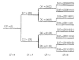
- OVSF codes are shown most clearly in a code tree structure.
- FIG. 1 shows an example of an OVSF code tree whose spreading factor ranges from 1 to 8.
- the code allocation rule for OVSF codes which ensures the orthogonality between the physical data transmission channels, is that, if a branch of the code tree is used for coding, all the preceding and succeeding branches in the tree structure are not permitted for further coding. If, by way of example, the code C 4,1 in the OVSF code tree shown in FIG. 1 is allocated for coding a channel, then the codes C 2,1 , C 1,1 , C 8,1 and C 8,2 are blocked until the allocated code C 4,1 has been released again.
- the invention achieves this object by means of a method having [lacuna] features specified in patent claim 1 and by means of an apparatus having the features specified in patent claim 6.
- the invention provides a method for generating an OVSF code word from code tree index data associated with a particular OVSF code within a prescribed OVSF tree, where a first code tree index data item (i) indicates the spreading factor of the OVSF code, and a second code tree index data item (j) indicates the position of the OVSF code among OVSF codes having the same spreading factor within the OVSF code tree, the method having the following steps:
- a calculation index is calculated on the basis of the second code tree index data item (j),
- the calculated calculation index is buffered as a binary data word having a plurality of data bits, the word length of the binary data word is calculated; the data bits of the data word are interchanged bit by bit in order to form a calculation base,
- the calculation base is logically combined with a counting variable in order to form a logically combined data word
- the logically combined data word is logically reduced in order to generate the OVSF code word.
- the calculation index is preferably calculated by subtracting 1 from the second code tree index data item (j).
- the calculation base is logically ANDed with the counting variable bit by bit.
- the logically combined data word is logically reduced by means of multistage XORing of adjacent data bits.
- the counting variable is generated by a modulo counter whose modulo base corresponds to the spreading factor of the OVSF code word which is to be generated.
- the invention also provides a code word generator for OVSF codes, having
- a buffer device for writing in a calculation index as a binary calculation index data word
- a calculation device which interchanges the data bits of the calculation index data word bit by bit in order to generate a calculation base
- a counter for generating a counting variable
- a logic circuit which has a plurality of AND gates for logically ANDing the generated counting variable with the calculation base bit by bit to form a logically combined data word, and a plurality of XOR gates for logically reducing the logically combined data word formed in order to form code word chips of the OVSF code word.
- the code word generator preferably has an input buffer for reading in a first code tree index data item index data item [sic] (i) and a second code tree index data item (j), the first code tree index data item (i) indicating the spreading factor of the OVSF code, and the second code tree index data item (j) indicating the position of the OVSF code among the OVSF codes having the same spreading factor within the OVSF code tree.
- a subtraction device which reduces the second code tree index data item (j) by 1 in order to calculate the calculation index.
- the counter is a modulo counter whose modulo counting base is adjustable.
- the modulo counting base corresponds to the spreading factor of the OVSF code word which is to be generated.
- a calculation unit is provided which is used for calculating the data word length of the calculation index data word.
- the calculated data word length of the calculation index data word is stored in a buffer.
- an output buffer is provided which buffers the code word data bits generated by the logic circuit in order to form the OVSF code word.
- the counter is preferably clocked at the code chip frequency.
- FIG. 1 shows the structure of an OVSF code tree
- FIG. 2 shows a block diagram of a CDMA transmission device for which the inventive code word generator for OVSF codes is used
- FIG. 3 shows a preferred embodiment of the inventive code word generator for OVSF codes
- FIG. 4 shows a logic reduction circuit forming part of the inventive code word generator for OVSF codes
- FIG. 5 shows a flowchart to explain the inventive method for generating OVSF code words.
- the inventive code word generator 1 for OVSF codes forms part of a CDMA transmission device.
- a data source 2 in the CDMA transmission device generates data symbols which are supplied to a spreading circuit 4 via a line 3 .
- the spreading circuit 4 is used for oversampling each data bit at an oversampling rate which corresponds to the spreading factor.
- the spread data are supplied via a line 5 to a multiplication device 6 , where the spread data are multiplied by the generated OVSF code word which is on the line 7 .
- the oversampled data bits and the generated OVSF code word bits with the value range ⁇ 0,1 ⁇ are converted or mapped to the antipodal value range ⁇ 1,+1 ⁇ before multiplication.
- the oversampled data bits and the generated OVSF code word bits are first logically combined with one another by a logic circuit and are then mapped or converted to the antipodal value range ⁇ 1;+1 ⁇ .
- the logic circuit is preferably an EXOR logic circuit or an equivalent logic circuit.
- the coded transmission signal formed in this manner is output by the multiplication device 6 to a signal conditioning circuit 9 via a line 8 .
- the signal conditioning circuit 9 conditions the coded transmission signal for transmission via the transmission channel.
- the conditioned transmission signal is output by the signal conditioning circuit 9 via the line 10 for further transmission.
- a clock generator 11 supplies a chip clock signal to the spreading circuit 4 and to the code word generator 1 via lines 12 , 13 .
- the code word generator 1 is connected to a signal bus 14 for data interchange with a DSP (Digital Signal Processor) or with a microcontroller.
- DSP Digital Signal Processor
- FIG. 3 shows a preferred embodiment of the inventive code word generator 1 .
- the code word generator 1 comprises two input registers 15 , 16 via which data are read in from the bus 14 .
- the input register 16 is used for buffering a calculation index as a binary calculation index data word.
- the input register 15 is used to store the data word length N of the calculation index data word buffered in the register 16 .
- the code word generator 1 also contains a calculation device 17 which interchanges the data bits of the calculation index data word buffered in the register 16 bit by bit in order to generate a calculation base.
- the calculation device 17 reads in, via data lines 18 , the calculation index data word stored in the storage register 16 , with the calculation device 17 receiving, via lines 19 , a control signal which indicates the data word length of the calculation index data word.
- Control lines 20 are used to set the modulo counting base N of a modulo counter 21 according to the data word length of the binary calculation index data word.
- the modulo counter 21 is supplied with the clock signal via the clock line 13 .
- the output of the modulo counter 21 is connected via data lines 22 to a logic circuit which comprises a plurality of AND gates 23 and also XOR gates 25 connected downstream via lines 24 .
- the AND gates 23 logically combine the output data bit lines 22 of the modulo counter 21 with data bit output lines 26 of the calculation device 17 bit by bit.
- the output data lines 26 carry the calculation base generated in the calculation device 17 .
- the AND gates 23 logically combine the counting variable which is on the output lines 22 with the calculation base which is on the lines 26 bit by bit to form a logically combined data word, which is logically reduced by the XOR gates 25 in order to form a code word data bit of the OVSF code word.
- the code word data bits generated bit by bit are stored via lines 26 in an output buffer 27 which outputs the generated OVSF code word to the multiplication device 6 via the line 7 .
- a code allocation algorithm first ascertains the OVSF code to be formed within the code tree structure.
- the OVSF code C 4,3 needs to be generated by the code generator 1 .
- the selected OVSF code is stipulated by its two code tree index data items i, j.
- the first code tree index data item i corresponds to the spreading factor of the OVSF code, for example 4, and the second code tree index data item j indicates the position of the OVSF code within those OVSF codes which have the same spreading factor within the OVSF code tree.
- a calculation index is ascertained for further calculation. In the case of the indexing chosen in FIG. 1, this is preferably done by subtracting 1 from the second code tree index data item j. The calculation index calculated in this manner is written to the input register 16 of the code word generator 1 via the bus 14 .
- the data word length of the calculation index N is calculated by forming the base two logarithm of the first code tree index data item i. If the OVSF code to be formed is C 4,3 and if the first code tree index data item i is thus 4 in line with the spreading factor, and if the second code tree index data item j is equal to 3 in line with the position of the OVSF code, the calculated calculation index is 2.
- the binary data length N of the calculated calculation index is likewise 2 and is written to the register 15 as a calculation index data word length N.
- the calculation device 17 for generating a calculation phase requires the data word length of the binary calculation index stored in the register 16 in order to interchange the data bits of the calculation index deliberately step by step.
- the calculation base generated by the calculation device 17 is logically ANDed bit by bit with the counting variable formed by the modulo counter 21 , using a plurality of AND gates.
- the base for the modulo counter is adjustable and corresponds to the spreading factor.
- the AND gates 23 form a binary logically combined data word which is supplied to a logic reduction circuit 25 via signal lines 24 .
- the data bits of the logically combined data word which are buffered in a register 28 , for example, are logically XORed in pairs starting with the least significant bit LSB using XOR gates 29 , 30 , 31 , 32 in order to form a code word data bit of the OVSF code word.
- the code word data bit formed by the logic reduction is passed via the line 26 to an output memory, in which the code word data bits formed are compiled to form the OVSF code word.
- the paired logical combination of the adjacent data bits of the logically combined data word formed by the logic AND circuit can also start with the most significant bit MSB.
- an OVSF code word by the inventive code word generator is shown using an example. If the allocation algorithm indicates the formation of the OVSF code C 4,3 with the first code word index data item 4 and the second code word index data item 3 , the calculation index and the word length N of the calculation index are first calculated.
- the calculation device 17 uses bit-by-bit interchange of the data bits of the calculation index data word to calculate the calculation base as 01.
- the modulo counting base for the modulo counter 21 is set to the word length N, and the counter is initialized to the initial count values 00.
- Logic reduction using XOR gates calculates the first code word chip bit Code 1 of the OVSF code word from this logically combined data word.
- a new logically combined data word Tmp is calculated by logic ANDing of the counter with the calculation base.
- Logic reduction of the logically combined data word calculates the next code word chip bit Code 2 of the OVSF code word and writes it to the output register 27 .
- the counter is then incremented again, the logically combined data word Tmp is formed and the third code word data bit of the OVSF code word is generated by logic XORing.
- the OVSF code word which is generated in this manner by the inventive code word generator 1 and is formed from the four generated code word chip bits (Code 1 -Code 4 ) corresponds to the code word prescribed by the code tree shown in FIG. 1 .
- the inventive code word generator 1 shown in FIG. 3 is very simple to implement in terms of circuitry, since it comprises merely registers 15 , 16 , a modulo counter 21 , a plurality of AND gates, a plurality of XOR gates and the calculation device 17 .
- the calculation device 17 can easily be implemented using shift registers and simple control logic.
- FIG. 5 shows a flowchart for the inventive method for generating an OVSF code word.
- a step S 1 the code tree index data items i, j for the desired OVSF codes are read in.
- the first code tree index data item i corresponds to the spreading factor of the OVSF code
- the second code word index data item j corresponds to the position of the position [sic] of the OVSF code.
- step S 2 a plurality of calculations are performed in step S 2 .
- a calculation index is calculated from the second code tree index data item j of the OVSF code by subtraction.
- the data word length N of the calculation index is likewise calculated in step S 2 .
- the calculation base B is also ascertained in step S 2 .
- the N significant bits of the calculation index are interchanged or swapped.
- step S 2 the modulo base for the modulo counter 21 is set in step, S 3 in line with the spreading factor SF of the OVSF code word which is to be generated, and the modulo counter is initialized to the initial count value 0.
- step S 4 the calculation base B formed by the calculation device 17 is logically combined and [sic] with the count value of the modulo counter 21 .
- the logical combination is performed bit by bit by a plurality of logic AND gates.
- the logic ANDing forms a logically combined data word which is logically reduced in step S 5 by a plurality of XOR gates 25 in order to form a code word data bit of the OVSF code word.
- step S 6 the code word data bit formed is written to the output memory 27 , and the modulo counter 21 is incremented.
- step S 8 a check is performed to determine whether the modulo counter has reached the initial initialization value 0 again and hence the loop has been performed sufficiently often in line with the spreading factor SF of the OVSF code word.
- step S 9 the OVSF code word compiled in the output memory 27 from the code word data bits formed is read out and is output to the multiplication device 6 via the line 7 shown in FIG. 2 .
- inventive code word generator for OVSF codes can be simplified further in terms of circuitry by virtue of the computational operations performed by the calculation device 17 being performed by the DSP processor connected to the bus 14 .
- the inventive method and the inventive generator for generating an OVSF code word can generate the associated OVSF code word from the code tree index data items i, j quickly and reliably without complex circuitry.
Landscapes
- Engineering & Computer Science (AREA)
- Computer Networks & Wireless Communication (AREA)
- Signal Processing (AREA)
- Compression, Expansion, Code Conversion, And Decoders (AREA)
Applications Claiming Priority (4)
| Application Number | Priority Date | Filing Date | Title |
|---|---|---|---|
| DE10004873 | 2000-02-04 | ||
| DE10004873.0 | 2000-02-04 | ||
| DE10004873A DE10004873A1 (de) | 2000-02-04 | 2000-02-04 | Verfahren und Vorrichtung zur Erzeugung von OVSF-Codeworten |
| PCT/EP2001/000668 WO2001058070A1 (de) | 2000-02-04 | 2001-01-22 | Verfahren und vorrichtung zur erzeugung von ovsf-codeworten |
Publications (2)
| Publication Number | Publication Date |
|---|---|
| US20030105532A1 US20030105532A1 (en) | 2003-06-05 |
| US6646579B2 true US6646579B2 (en) | 2003-11-11 |
Family
ID=7629780
Family Applications (1)
| Application Number | Title | Priority Date | Filing Date |
|---|---|---|---|
| US10/203,067 Expired - Fee Related US6646579B2 (en) | 2000-02-04 | 2001-01-22 | Method and device for generating OVSF code words |
Country Status (6)
| Country | Link |
|---|---|
| US (1) | US6646579B2 (de) |
| EP (1) | EP1252734A1 (de) |
| JP (1) | JP2003522473A (de) |
| CN (1) | CN1288863C (de) |
| DE (1) | DE10004873A1 (de) |
| WO (1) | WO2001058070A1 (de) |
Cited By (7)
| Publication number | Priority date | Publication date | Assignee | Title |
|---|---|---|---|---|
| US20020196936A1 (en) * | 2001-04-06 | 2002-12-26 | Interdigital Technology Corporation | System for generating pseudorandom sequences |
| US20030099282A1 (en) * | 2001-11-29 | 2003-05-29 | Per Olof Magnus Magnusson | Orthogonal variable spreading code (OVSF) allocation in telecommunications network |
| US20070041433A1 (en) * | 2005-08-18 | 2007-02-22 | Gongyu Zhou | Method and apparatus for compact OVSF despreading |
| US20070064590A1 (en) * | 2005-08-23 | 2007-03-22 | Tomasz Prokop | Buffer-based generation of OVSF code sequences |
| US20070070876A1 (en) * | 2005-09-27 | 2007-03-29 | Yen-Hui Yeh | Method and apparatus for ovsf code generation |
| US20080240596A1 (en) * | 2007-03-30 | 2008-10-02 | Haque Munsi A | Automatic generation of compact code tables |
| US8891351B2 (en) | 2011-09-26 | 2014-11-18 | Avago Technologies General Ip (Singapore) Pte. Ltd. | Orthogonal variable spreading factor code sequence generation |
Families Citing this family (8)
| Publication number | Priority date | Publication date | Assignee | Title |
|---|---|---|---|---|
| US6552996B2 (en) | 2001-09-18 | 2003-04-22 | Interdigital Communications Corporation | OVSF code system and methods |
| GB2381169B (en) * | 2001-10-15 | 2005-03-23 | Ubinetics Ltd | OVSF code generation |
| JP3896873B2 (ja) * | 2002-03-07 | 2007-03-22 | 日本電気株式会社 | 可変通信システム |
| KR100511294B1 (ko) * | 2002-10-26 | 2005-08-31 | 엘지전자 주식회사 | 비동기 코드분할 다중접속 통신 시스템의 심벌 매핑 및채널화 장치 |
| AU2003296841A1 (en) * | 2003-12-29 | 2005-08-12 | Pirelli Pneumatici S.P.A. | Method for manufacturing a tyre |
| CN1988428B (zh) * | 2005-12-23 | 2011-04-06 | 中兴通讯股份有限公司 | 宽带码分多址系统正交可变扩频因子码生成的方法和装置 |
| KR101459044B1 (ko) | 2008-01-10 | 2014-11-07 | 서강대학교산학협력단 | 무선 통신 시스템에서 이단 방식을 이용하여 효율적으로ovsf 코드를 생성하는 장치 및 방법 |
| FR3036203B1 (fr) | 2015-05-13 | 2017-05-19 | Inside Secure | Procede de securisation d’une comparaison de donnees lors de l’execution d’un programme |
Citations (7)
| Publication number | Priority date | Publication date | Assignee | Title |
|---|---|---|---|---|
| EP0814581A2 (de) | 1996-06-19 | 1997-12-29 | Ntt Mobile Communications Network Inc. | CDMA Nachrichtenübertragungsverfahren und Gruppenspreizmodulator |
| US5751761A (en) | 1993-07-20 | 1998-05-12 | Qualcomm Incorporated | System and method for orthogonal spread spectrum sequence generation in variable data rate systems |
| DE19835643A1 (de) | 1998-08-06 | 2000-02-10 | Siemens Ag | Verfahren und Einrichtung zur Kanalzuteilung in einem Kommunikationssystem mit CDMA-Teilnehmerseparierung |
| US6041034A (en) | 1996-12-20 | 2000-03-21 | Fujitsu Limited | Spread spectrum communication system |
| US6091757A (en) * | 1998-12-03 | 2000-07-18 | Motorola, Inc. | Data transmission within a spread-spectrum communication system |
| US6526065B1 (en) * | 1999-01-21 | 2003-02-25 | Industrial Technology Research Institute | Code management system and method for CDMA communication networks |
| US6552996B2 (en) * | 2001-09-18 | 2003-04-22 | Interdigital Communications Corporation | OVSF code system and methods |
Family Cites Families (1)
| Publication number | Priority date | Publication date | Assignee | Title |
|---|---|---|---|---|
| JPS6419052A (en) * | 1987-07-15 | 1989-01-23 | Nisshin Flour Milling Co | Production of l-methylosin |
-
2000
- 2000-02-04 DE DE10004873A patent/DE10004873A1/de not_active Withdrawn
-
2001
- 2001-01-22 WO PCT/EP2001/000668 patent/WO2001058070A1/de not_active Ceased
- 2001-01-22 CN CNB018042562A patent/CN1288863C/zh not_active Expired - Fee Related
- 2001-01-22 US US10/203,067 patent/US6646579B2/en not_active Expired - Fee Related
- 2001-01-22 JP JP2001557213A patent/JP2003522473A/ja active Pending
- 2001-01-22 EP EP01900474A patent/EP1252734A1/de not_active Withdrawn
Patent Citations (7)
| Publication number | Priority date | Publication date | Assignee | Title |
|---|---|---|---|---|
| US5751761A (en) | 1993-07-20 | 1998-05-12 | Qualcomm Incorporated | System and method for orthogonal spread spectrum sequence generation in variable data rate systems |
| EP0814581A2 (de) | 1996-06-19 | 1997-12-29 | Ntt Mobile Communications Network Inc. | CDMA Nachrichtenübertragungsverfahren und Gruppenspreizmodulator |
| US6041034A (en) | 1996-12-20 | 2000-03-21 | Fujitsu Limited | Spread spectrum communication system |
| DE19835643A1 (de) | 1998-08-06 | 2000-02-10 | Siemens Ag | Verfahren und Einrichtung zur Kanalzuteilung in einem Kommunikationssystem mit CDMA-Teilnehmerseparierung |
| US6091757A (en) * | 1998-12-03 | 2000-07-18 | Motorola, Inc. | Data transmission within a spread-spectrum communication system |
| US6526065B1 (en) * | 1999-01-21 | 2003-02-25 | Industrial Technology Research Institute | Code management system and method for CDMA communication networks |
| US6552996B2 (en) * | 2001-09-18 | 2003-04-22 | Interdigital Communications Corporation | OVSF code system and methods |
Cited By (17)
| Publication number | Priority date | Publication date | Assignee | Title |
|---|---|---|---|---|
| US7643638B2 (en) * | 2001-04-06 | 2010-01-05 | Interdigital Technology Corporation | System for generating pseudorandom sequences |
| US20020196936A1 (en) * | 2001-04-06 | 2002-12-26 | Interdigital Technology Corporation | System for generating pseudorandom sequences |
| US7248698B2 (en) * | 2001-04-06 | 2007-07-24 | Interdigital Technology Corporation | System for generating pseudorandom sequences |
| US20070258593A1 (en) * | 2001-04-06 | 2007-11-08 | Interdigital Technology Corporation | System for generating pseudorandom sequences |
| US20030099282A1 (en) * | 2001-11-29 | 2003-05-29 | Per Olof Magnus Magnusson | Orthogonal variable spreading code (OVSF) allocation in telecommunications network |
| US7054294B2 (en) * | 2001-11-29 | 2006-05-30 | Telefonaktiebolaget Lm Ericsson (Publ) | Orthogonal variable spreading code (OVSF) allocation telecommunications network |
| US20070041433A1 (en) * | 2005-08-18 | 2007-02-22 | Gongyu Zhou | Method and apparatus for compact OVSF despreading |
| US7706427B2 (en) * | 2005-08-18 | 2010-04-27 | Agere Systems Inc. | Method and apparatus for compact OVSF despreading |
| US7894327B2 (en) * | 2005-08-23 | 2011-02-22 | Agere Systems Inc. | Buffer-based generation of OVSF code sequences |
| US20070064590A1 (en) * | 2005-08-23 | 2007-03-22 | Tomasz Prokop | Buffer-based generation of OVSF code sequences |
| US20110110399A1 (en) * | 2005-08-23 | 2011-05-12 | Agere Systems | Buffer-based generation of ovsf code sequences |
| US8462614B2 (en) * | 2005-08-23 | 2013-06-11 | Agere Systems Llc | Buffer-based generation of OVSF code sequences |
| US20070070876A1 (en) * | 2005-09-27 | 2007-03-29 | Yen-Hui Yeh | Method and apparatus for ovsf code generation |
| US7729235B2 (en) | 2005-09-27 | 2010-06-01 | Mediatek Inc. | Method and apparatus for OVSF code generation |
| US20080240596A1 (en) * | 2007-03-30 | 2008-10-02 | Haque Munsi A | Automatic generation of compact code tables |
| US7970215B2 (en) * | 2007-03-30 | 2011-06-28 | Intel Corporation | Automatic generation of compact code tables |
| US8891351B2 (en) | 2011-09-26 | 2014-11-18 | Avago Technologies General Ip (Singapore) Pte. Ltd. | Orthogonal variable spreading factor code sequence generation |
Also Published As
| Publication number | Publication date |
|---|---|
| US20030105532A1 (en) | 2003-06-05 |
| JP2003522473A (ja) | 2003-07-22 |
| WO2001058070A1 (de) | 2001-08-09 |
| CN1397121A (zh) | 2003-02-12 |
| EP1252734A1 (de) | 2002-10-30 |
| DE10004873A1 (de) | 2001-08-23 |
| CN1288863C (zh) | 2006-12-06 |
Similar Documents
| Publication | Publication Date | Title |
|---|---|---|
| US6646579B2 (en) | Method and device for generating OVSF code words | |
| US6636553B1 (en) | Pseudorandom noise generator for WCDMA | |
| US5311176A (en) | Method and apparatus for generating Walsh codes | |
| KR100335038B1 (ko) | 코드분할다중접속시스템어플리케이션용다중속도직렬비터비디코더 | |
| Pupeza et al. | Efficient generation of interleavers for IDMA | |
| US20080281892A1 (en) | Method and Apparatus for Generating Pseudo Random Numbers | |
| US6636549B1 (en) | Method for calculating phase shift coefficients of an M sequence | |
| US8462614B2 (en) | Buffer-based generation of OVSF code sequences | |
| KR100607376B1 (ko) | 의사-랜덤 수 시퀀스 발생기 및 이와 관련된 방법 | |
| KR100525799B1 (ko) | 주파수도약수열 발생장치 | |
| EP2827516B1 (de) | Verfahren und vorrichtung zur erzeugung eines verschlüsselungscodes und vorrichtung zur verarbeitung eines verschlüsselungscodes | |
| KR20040085545A (ko) | 통신 시스템에서 오류 정정 부호의 복호 장치 및 방법 | |
| CN100423463C (zh) | 计算回馈位移寄存器装置叠代状态的方法及装置 | |
| KR100327856B1 (ko) | M계열을 임의로 쉬프트하는 회로 및 방법 | |
| US7324581B2 (en) | Apparatus for mapping and spreading data symbols in mobile communication system | |
| US7317776B2 (en) | Efficient pseudo-noise sequence generation for spread spectrum applications | |
| KR100308887B1 (ko) | 계층화된 직교부호 발생장치 및 그 방법 | |
| KR100307705B1 (ko) | 계층화된 직교부호 발생장치 및 그 방법 | |
| KR101459044B1 (ko) | 무선 통신 시스템에서 이단 방식을 이용하여 효율적으로ovsf 코드를 생성하는 장치 및 방법 | |
| KR0147327B1 (ko) | 무상관 자기 합산 난수 발생 장치 | |
| KR100275527B1 (ko) | 워드 난수 발생 장치 및 그 방법 | |
| KR100399199B1 (ko) | 가변 복잡도를 갖는 선택적 확산 코드 발생 장치 및 방법 | |
| JP3790514B2 (ja) | 疑似ランダムシーケンス生成システム | |
| KR100338635B1 (ko) | 다단계 채널 인터리버/디인터리버에 사용하기 위한어드레스 생성 장치 및 방법 | |
| JP2000278099A (ja) | M系列発生回路及びpn符号発生回路 |
Legal Events
| Date | Code | Title | Description |
|---|---|---|---|
| AS | Assignment |
Owner name: INFINEON TECHNOLOGIES AG, GERMANY Free format text: ASSIGNMENT OF ASSIGNORS INTEREST;ASSIGNORS:DOETSCH, MARKUS;FEYFANT, PATRICK;JUNG, PETER;AND OTHERS;REEL/FRAME:013312/0852;SIGNING DATES FROM 20020717 TO 20020812 |
|
| FEPP | Fee payment procedure |
Free format text: PAYOR NUMBER ASSIGNED (ORIGINAL EVENT CODE: ASPN); ENTITY STATUS OF PATENT OWNER: LARGE ENTITY |
|
| REMI | Maintenance fee reminder mailed | ||
| LAPS | Lapse for failure to pay maintenance fees | ||
| STCH | Information on status: patent discontinuation |
Free format text: PATENT EXPIRED DUE TO NONPAYMENT OF MAINTENANCE FEES UNDER 37 CFR 1.362 |
|
| FP | Lapsed due to failure to pay maintenance fee |
Effective date: 20071111 |