US6646224B2 - Plasma-assisted processing system and plasma-assisted processing method - Google Patents
Plasma-assisted processing system and plasma-assisted processing method Download PDFInfo
- Publication number
- US6646224B2 US6646224B2 US10/356,639 US35663903A US6646224B2 US 6646224 B2 US6646224 B2 US 6646224B2 US 35663903 A US35663903 A US 35663903A US 6646224 B2 US6646224 B2 US 6646224B2
- Authority
- US
- United States
- Prior art keywords
- plasma
- level
- frequency wave
- antenna
- vacuum vessel
- Prior art date
- Legal status (The legal status is an assumption and is not a legal conclusion. Google has not performed a legal analysis and makes no representation as to the accuracy of the status listed.)
- Expired - Fee Related
Links
Images


Classifications
-
- H—ELECTRICITY
- H01—ELECTRIC ELEMENTS
- H01J—ELECTRIC DISCHARGE TUBES OR DISCHARGE LAMPS
- H01J37/00—Discharge tubes with provision for introducing objects or material to be exposed to the discharge, e.g. for the purpose of examination or processing thereof
- H01J37/32—Gas-filled discharge tubes
- H01J37/32009—Arrangements for generation of plasma specially adapted for examination or treatment of objects, e.g. plasma sources
- H01J37/32082—Radio frequency generated discharge
- H01J37/321—Radio frequency generated discharge the radio frequency energy being inductively coupled to the plasma
-
- H—ELECTRICITY
- H01—ELECTRIC ELEMENTS
- H01J—ELECTRIC DISCHARGE TUBES OR DISCHARGE LAMPS
- H01J37/00—Discharge tubes with provision for introducing objects or material to be exposed to the discharge, e.g. for the purpose of examination or processing thereof
- H01J37/32—Gas-filled discharge tubes
- H01J37/32009—Arrangements for generation of plasma specially adapted for examination or treatment of objects, e.g. plasma sources
- H01J37/32082—Radio frequency generated discharge
-
- H—ELECTRICITY
- H01—ELECTRIC ELEMENTS
- H01J—ELECTRIC DISCHARGE TUBES OR DISCHARGE LAMPS
- H01J37/00—Discharge tubes with provision for introducing objects or material to be exposed to the discharge, e.g. for the purpose of examination or processing thereof
- H01J37/32—Gas-filled discharge tubes
- H01J37/32431—Constructional details of the reactor
- H01J37/32532—Electrodes
- H01J37/32568—Relative arrangement or disposition of electrodes; moving means
Definitions
- the present invention relates to a plasma-assisted processing system and a plasma-assisted processing method that produce a plasma by using the energy of a high-frequency wave, such as a microwave, and use the plasma for processing a substrate, such as a semiconductor wafer.
- a high-frequency wave such as a microwave
- a semiconductor device manufacturing process includes a step of processing a semiconductor wafer (hereinafter referred to simply as “wafer”) by using a plasma
- FIG. 16 shows a known microwave plasma-assisted processing system that carries out a plasma-assisted process.
- the microwave plasma-assisted processing system has a vacuum vessel 9 provided with a stage 91 for supporting a wafer W thereon, a planar slot antenna 92 disposed in a ceiling region of the vacuum vessel 9 , a microwave power unit 93 , a coaxial waveguide 94 provided with a shaft 94 a and connected to the microwave source 93 and the vacuum vessel 9 , a microwave transmitting plate 95 of quartz, and a gas supply unit 96 .
- a microwave generated by the microwave power unit 93 is guided through the waveguide 94 , the antenna 92 and the microwave transmitting plate 95 into the vacuum vessel 9 , a process gas supplied by the gas supply unit 96 into the vacuum vessel 9 is ionized by the microwave to produce a plasma, and the plasma is used for forming a film on the wafer W or for etching a film formed on the wafer W.
- a plasma is a complicated combination of electrical, physical and chemical phenomena and its mechanism has many points which have not yet been elucidated. As matters stand, the dependence of the condition of a plasma on process conditions has not been definitely elucidated. Therefore, even if a highly uniform plasma can be produced under certain process conditions including pressure and power of a microwave, sometimes, the uniformity of the plasma is deteriorated under other process conditions.
- the uniformity of a plasma is reflected directly on the uniformity of a film thickness or the uniformity of etch rate. Since the recent semiconductor devices are miniaturized and are provided with thin films, the yield of semiconductor devices is greatly dependent on the uniformity of the plasma. Accordingly, the development of techniques capable of producing a highly uniform plasma regardless of process conditions has been desired.
- a plasma-assisted processing system comprising a vacuum vessel internally provided with a stage, a high-frequency wave transmitting plate attached to the vacuum vessel, a planar antenna disposed opposite to the high-frequency wave transmitting plate, and a high-frequency power unit that sends a high-frequency wave for producing a plasma to the antenna, and capable of propagating a high-frequency wave for producing a plasma through the antenna and the high-frequency wave transmitting plate into the vacuum vessel, of producing a plasma by ionizing a processing gas supplied into the vacuum vessel by the energy of the high-frequency wave and of processing a substrate mounted on the stage in the vacuum vessel by using the plasma; comprises: a lifting mechanism that moves the antenna vertically relative to the vacuum vessel; an electromagnetic shielding member surrounding a region between the antenna and the high-frequency wave transmitting plate; a level estimating unit that estimates a level of high-frequency wave cutoff density formed between the high-frequency wave transmitting plate and a plasma producing region; and a controller that controls the
- the level of the antenna can be properly adjusted on the basis of the result of operation of the level estimating unit by determining the proper size of the cavity beforehand.
- the level estimating unit includes a transparent plate covering an opening formed in a side wall of the vacuum vessel, and a cease region detecting unit capable of optically detecting a lower limit level of a cease region in which a plasma produced in the plasma producing region ceases between the high-frequency wave transmitting plate and a region in which the plasma is luminescent, and the level of the cutoff density is estimated on the basis of the detected lower limit level for the cease region.
- the level estimating unit includes a high-frequency wave radiating unit that delivers a detecting high-frequency wave from above the plasma to the plasma, and a high-frequency wave receiving unit that receives the detecting high-frequency wave delivered to and reflected by the plasma, a level of the cutoff density for the detecting high-frequency wave is determined on the basis of a position of the reflected high-frequency wave on the high-frequency wave receiving unit, and a level of the cutoff density for the plasma producing high-frequency wave is estimated on the basis of the level of the cutoff density for the detecting high-frequency wave.
- the level of a cutoff density for the plasma producing high-frequency wave and the lower limit level of the cease region are different from each other, the difference between those levels can be regarded as substantially fixed. Therefore, those results of detection can be used in substitution for the level of a cutoff density for the plasma producing high-frequency wave.
- Estimation of the level of a cutoff density for the high-frequency wave includes the use of the detected lower limit level of the cease region of the plasma and the detected level of a cutoff density for the detecting high-frequency wave as substitutes, and includes the estimation of the level of a cutoff density for the plasma producing high-frequency wave on the basis of a predetermined algorithm.
- a plasma-assisted processing system comprising a vacuum vessel internally provided with a stage, a high-frequency wave transmitting plate attached to the vacuum vessel, a planar antenna disposed opposite to the high-frequency wave transmitting plate, and a high-frequency power unit that delivers a high-frequency wave for producing a plasma to the antenna, and capable of propagating a high-frequency wave for producing a plasma through the antenna and the high-frequency wave transmitting plate into the vacuum vessel, of producing a plasma by ionizing a processing gas supplied into the vacuum vessel by the energy of the high-frequency wave and of processing a substrate mounted on the stage in the vacuum vessel by using the plasma; comprises: a lifting mechanism that moves the antenna vertically relative to the vacuum vessel; an electromagnetic shielding member surrounding a region between the antenna and the high-frequency wave transmitting plate; a storage unit that stores set antenna levels for recipes for plasma-assisted process; and a controller that reads a level of the antenna for a selected recipe from the storage unit and controls the
- a plasma-assisted processing method comprises the steps of: propagating a plasma producing high-frequency wave delivered by a high-frequency power unit through a planar antenna and a high-frequency wave transmitting plate into a vacuum vessel; producing a plasma by ionizing a processing gas supplied into the vacuum vessel by the energy of the high-frequency wave; and processing a substrate supported on a stage disposed in the vacuum vessel; wherein the substrate is processed by a plasma-assisted process after adjusting the level of the antenna relative to the vacuum vessel so that a cavity region of a proper size for the high-frequency wave is formed between the antenna and a level of a cutoff density for the high-frequency wave in the vacuum vessel.
- FIGS. 1A and 1B are views of assistance in explaining results of observation of a plasma
- FIG. 2 is a graph showing an ion current intensity distribution in a plasma
- FIG. 3 is a typical view of a cavity for a microwave
- FIG. 4 is a graph showing the variation of electron density with the position of a microwave in a vacuum vessel relative to a microwave transmitting plate
- FIG. 5 is a typical view of assistance in explaining the reflection of a microwave at a position of a cutoff density for an X-wave;
- FIG. 6 is a table of assistance in explaining the relation between process conditions and position of a cutoff density for an X-wave;
- FIG. 7 is a schematic longitudinal sectional view of a plasma-assisted processing system in a first embodiment according to the present invention.
- FIG. 8 is an enlarged sectional view of a portion of the plasma-assisted processing system shown in FIG. 7;
- FIG. 9 is view of assistance in explaining a cavity for a microwave before and after the adjustment of the level of an antenna
- FIGS. 10, 11 and 12 are graphs showing electron density distributions in a processing vessel under different conditions
- FIG. 13 is a block diagram of a control system included in a plasma-assisted processing system in a second embodiment according to the present invention.
- FIG. 14 is a typical view of assistance in explaining the resonance of electric field intensity distributions respectively over and under a microwave transmitting plate
- FIGS. 15A and 15B are views of assistance in explaining the shape of a cross section of a wall between an upper part of a microwave transmitting plate and a vacuum chamber;
- FIG. 16 is a schematic longitudinal sectional view of a conventional plasma-assisted processing system.
- a plasma produced in the vacuum vessel 9 included in the conventional plasma-assisted processing system shown in FIG. 16 was observed by using a CCD camera embedded in the stage 91 disposed in the vacuum vessel 9 and having an upper part formed of quartz.
- Argon gas was supplied from the gas supply unit 96 into the vacuum vessel 9 and a 2.45 GHz microwave was propagated from the microwave power unit 93 into the vacuum vessel 9 to produce a plasma by ionizing the argon gas.
- the power of the microwave and the pressure in the vacuum vessel 9 were varied and the condition of the plasma was observed.
- the brightness of the plasma was uniform under some conditions and was irregular under other conditions.
- FIGS. 1A and 1B are views showing images of plasmas taken by the CCD camera.
- FIG. 1A shows an irregular plasma having particularly bright regions and
- FIG. 1B shows a uniform plasma having uniform brightness.
- Table 1 shows process conditions and the condition of plasmas.
- Ion current intensity distribution in the vacuum vessel 9 with respect to radial directions was measured under the foregoing process conditions. Measured results are shown in FIG. 2 .
- ion current intensity increases from a position on the wall of the vacuum vessel 9 toward the center of the same.
- Ion current intensity distributions under the process conditions B and C are substantially the same; ion current intensity under the process conditions B and C is substantially on the same level between the wall of the vacuum vessel 9 and the center of the same.
- the ion current intensity distributions under the process conditions B and C are indicated by a single curve for the sake of convenience.
- Ion current intensity is dependent on the electron density of the plasma.
- the size of a plasma cease region i.e., a region near the wall in which the plasma is not luminescent, is dependent on electron density.
- the inventors of the present invention noticed a fact that the size of the plasma cease region is related with the size of a microwave cavity extending over the plasma.
- the cavity is formed between the antenna 92 and a position of a cutoff density for the microwave.
- shaded region S is a cavity.
- FIG. 4 is a graph showing the variation of electron density with distance from the lower surface of the microwave transmitting plate 95 in the vacuum vessel 9 .
- a cutoff density X 0 for the plasma producing microwave is at a position at a certain distance from the microwave transmitting plate 95 .
- level X0 the level of the cutoff density X 0
- the plasma producing microwave falling from above the level X 0 is reflected.
- a portion of the plasma near the wall of the vacuum vessel 9 is in a cease region in which the plasma is not luminescent.
- the level X 0 is below a level L 0 of the lower limit of the cease region (hereinafter referred to as “cease level L0”), and the difference between those levels is substantially constant.
- the level X 0 can be determined, for example, by radiating an electromagnetic wave obliquely downward toward, for example, a central region of the vacuum vessel 9 by an electromagnetic wave radiator 97 disposed on an electromagnetic shielding member extending between the antenna 92 and the microwave transmitting plate 95 as shown in FIG. 5, receiving the reflected electromagnetic wave by an electromagnetic wave receiver 98 , and calculating the level of a position from which the electromagnetic wave is reflected on the basis of a position at which the reflected electromagnetic wave falls on the electromagnetic wave receiver 98 .
- the electromagnetic wave receiver When a microwave of the same frequency as that of the plasma producing microwave is radiated by the electromagnetic wave radiator 97 , the electromagnetic wave receiver is unable to discriminate between the microwave radiated by the electromagnetic wave radiator 97 and the plasma producing microwave radiated by the antenna 92 . Therefore, a measuring microwave of a frequency different from that of the plasma producing microwave is radiated by the electromagnetic wave radiator 97 .
- the level of a cutoff density for the measuring microwave (hereinafter referred to as “level X1”) can be determined.
- the frequency of the measuring microwave is, for example, in the range of several gigahertz to about 30 GHz.
- the lower limit frequency when considered in connection with the shape of the vacuum chamber, is on the order of several gigahertz. Since frequency is proportional to the square root of cutoff density (electron density), the upper limit frequency is on the order of 30 GHz at the highest.
- the electromagnetic wave receiver 98 may comprise a plurality of wave receiving elements in a vertical arrangement and may estimate the position of the reflected electromagnetic wave on the basis of the position of the wave receiving element that receives the electromagnetic wave or may comprise a single wave receiving element that is moved vertically for scanning and may estimate the position of the reflected electromagnetic wave from a position where the scanning wave receiving element receives the reflected electromagnetic wave. Since the interval between the level X 0 and the cease level, the cease level may be detected optically and may be used in substitution for the level X 0 .
- Level X0 signifies distance from the lower surface of the microwave transmitting plate 95 to the level X 0 .
- the level X 0 approaches the microwave transmitting plate 95 as the power of the microwave increases, and the level X 0 approaches the microwave transmitting plate 95 as the pressure increases.
- a cavity of a proper size is formed by determining a proper size of a cavity beforehand, detecting the position of the level X 0 when carrying out a process, and adjusting the height of the antenna 92 . Since the position of the level X 0 changes scarcely when the height of the antenna 92 is changed under some process conditions, adjustment is made so that distance between the antenna 92 and the level X 0 coincides with the vertical length of the proper cavity.
- the plasma-assisted processing system has a vacuum vessel 1 of, for example, a cylindrical shape, and a stage 2 disposed in the vacuum vessel 1 to support a wafer W, i.e., a substrate, thereon.
- a discharge pipe 11 through which the vacuum vessel 1 is evacuated is connected to the bottom wall of the vacuum vessel 1 .
- An electrode 22 is embedded in the stage 2 and is connected to a high-frequency bias power unit 21 to apply, for example, a 13.56 MHz bias voltage to the stage 2 .
- the stage 2 is provided with a temperature adjusting unit, not shown, to adjust the temperature of the wafer W to a predetermined temperature.
- An open end of the vacuum vessel 1 is covered with a microwave transmitting plate 23 of a dielectric material, such as quartz.
- a planar antenna 32 provided with a plurality of slots 31 is disposed opposite to the microwave transmitting plate 23 .
- a coaxial waveguide 33 has an inner pipe 33 a and an outer pipe 33 b coaxially surrounding the inner pipe 33 a .
- One end of the inner pipe 33 a of the coaxial waveguide 33 is connected to a central part of the antenna 32 .
- a lower end part of the outer pipe 33 b is expanded radially and extended axially downward to form a flat, cylindrical part 34 .
- a rectangular waveguide 35 has one end connected to the side surface of one end of the coaxial waveguide 33 remote from the antenna 32 , and the other end connected through an impedance matching unit, not shown, to a microwave power unit 36 .
- the microwave power unit 36 is held on a holding table 41 which can be vertically moved by a lifting mechanism 4 .
- the microwave power unit 36 and the waveguides 33 and 35 can be vertically moved by the lifting mechanism 4 .
- the lifting mechanism 4 may be, for example, a motor-driven jack or a lifting device employing a ball screw and a pneumatic cylinder actuator.
- An electromagnetic shielding cylinder 42 of a metal is set up on a peripheral part of the microwave transmitting plate 23 .
- An annular plate spring 43 having a U-shaped cross section is fitted in an annular space between the inner surface of the shielding cylinder 42 and the outer surface of the expanded part 34 of the waveguide 33 . Since the waveguide 33 can be vertically movable as mentioned above, the plate spring 43 separates a space under the antenna 32 from a space around the waveguide 33 and guides the expanded part 34 .
- the inner pipe 34 of the waveguide 33 is cylindrical.
- a gas supply pipe 5 is extended through the inner pipe 34 .
- an opening 24 is formed in a central part of the microwave transmitting plate 23 and a metal ring 51 is fitted in the opening 24 .
- the free end of the gas supply pipe 5 is welded to a flange formed on the metal ring 51 .
- a telescopic electromagnetic shielding device 52 is disposed below the inner pipe 33 a so as to surround the gas supply pipe 5 .
- the electromagnetic shielding member 52 is formed by sequentially nesting a plurality of metal cylinders 52 a , 52 b and 52 c one in one another.
- the gas supply pipe 5 is extended through the inner pipe 33 a so as to be movable relative to the inner pipe 33 a and the outer pipe 33 b .
- the waveguide 33 can be moved vertically with the gas supply pipe 5 fixed.
- a transparent plate 61 of, for example, quartz is fitted in an opening formed in the side wall of the vacuum vessel 1 and a cease level detector 62 for detecting the cease level (the lower limit level of a cease region) is disposed on the outer surface of the transparent plate 61 .
- the cease level detector 62 may be an light sensor array of a plurality of light sensors vertically arranged with their optical axes extended horizontally. The light sensors corresponding to regions in which the plasma is luminescent are on and those corresponding to a cease region are off. Thus, a cease level can be detected by the cease level detector 62 .
- a controller 63 receives a detection signal from the cease level detector 62 and a level signal from the lifting mechanism 4 .
- the controller 63 finds the level of the antenna 32 on the basis of a pulse signal generated by an encoder connected to a motor included in the lifting mechanism 4 .
- the controller 63 calculates a distance by which the antenna 32 must be vertically moved on the basis of the level of the antenna and the cease level and gives a control signal to the lifting mechanism 4 to move the antenna 32 by the calculated distance.
- the proper size of a cavity for the microwave for processing a wafer W by a plasma-assisted process such as a plasma-assisted film forming process for forming a polysilicon film on the wafer W, is determined beforehand.
- a cavity suitable for producing a plasma of uniform brightness may be determined through the observation of the plasma using the CCD camera.
- the cavity of the proper size is stored in the controller 63 .
- the size of the cavity extends, on definition, between the antenna 32 and the level X 0 . Since the distance between the cease level and the level X 0 is substantially fixed, storage of the proper distance H between the antenna 32 and the cease level is substantially equivalent to storage of the size of the cavity when the height of the antenna 32 is controlled through the detection of the cease level.
- FIG. 9 is a view of assistance in explaining the adjustment of the level of the antenna 32 .
- the height of a cavity i.e., a region between the antenna 32 and the cease level L 0
- the height of the antenna 32 is reduced by h 1 (the level X 0 remains unchanged) to reduce the height of the cavity to H.
- the level X 1 of a cutoff density for the measuring microwave is detected by the same procedure, in which the distance between the antenna and the level X 1 is H.
- the cease level detector 62 and the controller 63 serve as a level estimating unit that estimates the level X 0 .
- the electromagnetic wave radiator 97 and the electromagnetic wave receiver 98 shown in FIG. 5 are used for detecting the level X 1
- the electromagnetic wave radiator 97 , the electromagnetic wave receiver 98 and the controller serve as a level estimating unit that estimates the level X 0 .
- Estimation of the level X 0 includes using the cease level L 0 or the detected level X 1 in substitution for the level X 0 , and estimating the level X 0 by using an algorithm on the basis of the cease level L 0 or the detected level X 1 .
- a wafer W is carried into the vacuum vessel 1 and is mounted on the stage 2 .
- the vacuum vessel 1 is evacuated to a predetermined vacuum of, for example, 10 ⁇ 6 torr and monosilane (SiH 4 ) gas, i.e., a film forming gas, and Ar gas, i.e., a carrier gas, are supplied into the vacuum vessel 1 .
- the microwave power unit 36 delivers plasma producing microwave power of, for example, 2.45 GHz and 2.5 kW and the bias power unit 21 applies bias power of, for example, 13.56 MHz and 1.5 kW to the stage 2 .
- the microwave generated by the microwave power unit 36 is guided for propagation by the waveguides 35 and 33 to the expanded part 34 and is propagated through the slots 31 of the antenna 32 into the vacuum vessel 1 .
- the microwave ionizes the monosilane gas to produce active species, and the active species are deposited on a surface of the wafer W to form a polysilicon film.
- the level of the antenna is adjusted by the foregoing procedure before processing wafers W.
- the proper size H of the cavity is measure beforehand by using a processing gas to be used, such as monosilane gas. If the proper sizes of cavities for different gases are similar, the measured size may be used as the proper size H.
- the plasma can be produced in a high uniformity at all times and the substrate can be processed in a high intrasurface uniformity, for example, to form a film of a uniform thickness on the wafer.
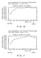
- FIGS. 10 to 12 show the results of experiments conducted by using the plasma-assisted processing system shown in FIG. 7 to examine the effect of the level of the antenna 32 on electron density.
- Ar gas was supplied into the vacuum vessel 1 and the pressure in the vacuum vessel was adjusted to 30 mtorr (3.99 Pa), a plasma was produced by delivering 2.45 GHz, 2 kW microwave power by the microwave power unit 36 and applying 13.56 MHz, 1.5 kW bias power to the stage 2 by the bias power unit 21 , and a region at 10.5 cm from the lower surface of the microwave transmitting plate 23 was scanned along a diameter of the vacuum vessel 1 with a probe to measure electron densities.
- FIG. 10 shows the results of experiments conducted by using the plasma-assisted processing system shown in FIG. 7 to examine the effect of the level of the antenna 32 on electron density.
- a point at 0.0 on the horizontal axis corresponds to a position on the side wall of the vacuum vessel and a point at 27.0 on the horizontal axis corresponds to the center of the vacuum vessel 1 .
- the cease level rises i.e., the cease level approaches the microwave transmitting plate 23 , when the gas pressure is increased to increase the density of the plasma and hence a uniform plasma can be produced by raising the level of the antenna 32 to secure a proper distance between the antenna 32 and the plasma.
- the vacuum vessel 1 may be moved vertically instead of moving the antenna 32 .
- the plasma-assisted process may be an etching process or an ashing process.
- An RF power unit or a UHF power unit may be used for ionizing a processing gas instead of the microwave power unit.
- microwave power units, RF power units and UHF power units are called inclusively high-frequency power units.
- a plasma may be produced by ionizing a processing gas by the electron cyclotron resonance of a microwave and a magnetic field.
- levels of antenna 32 suitable for forming cavities of proper sizes for recipes may be determined and stored in a storage unit 71 beforehand, a CPU 73 may read a level of the antenna 32 for a recipe selected by a recipe selecting unit 72 , a controller 74 may give a control signal to the lifting mechanism 4 to set the antenna 32 on the level read by the CPU 73 .
- the proper level of the antenna 32 may be determined on the basis of the previously determined proper size H of the cavity by detecting a cease level for each recipe or may be determined by adjusting the level of the antenna 32 for each recipe observing the condition of the process.
- the antenna 32 may be vertically moved by a metal bellows extended between a peripheral part of the antenna 32 and a peripheral part of the microwave transmitting plate 23 .
- the wall part 40 and the antenna 32 may be formed respectively in shapes having hexagonal cross sections and the vacuum vessel 1 may be formed in a cylindrical shape having a circular cross section, or the wall part 40 and the antenna 32 may be formed respectively in cylindrical shapes and the vacuum vessel 1 may be formed in a shape having a polygonal cross section as shown in FIG. 15 A.
- Both the vacuum vessel 1 and the electromagnetic shielding cylinder 42 may be formed respectively in shapes having n-sided polygonal cross sections (in FIG. 6, hexagonal cross sections) and may be disposed with the corners thereof circumferentially dislocated relative to each other as shown in FIG. 15 B.
- the vacuum vessel 1 and the electromagnetic shielding cylinder 42 may be formed respectively in shapes having special curvilinear cross sections other than polygonal cross sections.
- the wall part 40 and the vacuum vessel 1 are formed in shapes having different cross sections, respectively, the wall part 40 and the vacuum vessel 1 have different microwave modes, respectively, whereby the emphasis of the electric field intensity distribution can be reduced or avoided and the uniformity of the plasma can be improved.
- a highly uniform plasma can be produced and a substrate can be processed in a high intrasurface uniformity.
Landscapes
- Physics & Mathematics (AREA)
- Engineering & Computer Science (AREA)
- Plasma & Fusion (AREA)
- Chemical & Material Sciences (AREA)
- Analytical Chemistry (AREA)
- Plasma Technology (AREA)
- Chemical Vapour Deposition (AREA)
Abstract
A plasma-assisted processing system has a lifting mechanism capable of vertically moving a microwave power unit and a waveguide to adjust the level of a planar slot antenna disposed on an expanded lower end part of the waveguide. A space extending under the antenna is surrounded by a shielding member. An optical sensor having an array of photosensors is disposed on the outer side of a window formed in the side wall of a vacuum vessel to monitor the lower limit level of a cease region for a plasma (cease level). An ideal distance between the cease level and the antenna is determined beforehand and the level of the antenna is adjusted on the basis of a measured cease level so that the antenna is spaced the ideal distance apart from the cease level. Since the difference between the cease level and a level X0 for the cutoff density of an X-wave is fixed, the level X0 may be monitored instead of the cease level.
Description
This is a divisional of application Ser. No. 09/595,476, filed Jun. 16, 2000 now U.S. Pat. No. 6,528,752, which is incorporated herein by reference.
1. Field of the Invention
The present invention relates to a plasma-assisted processing system and a plasma-assisted processing method that produce a plasma by using the energy of a high-frequency wave, such as a microwave, and use the plasma for processing a substrate, such as a semiconductor wafer.
2. Description of the Related Art
A semiconductor device manufacturing process includes a step of processing a semiconductor wafer (hereinafter referred to simply as “wafer”) by using a plasma FIG. 16 shows a known microwave plasma-assisted processing system that carries out a plasma-assisted process. As shown in FIG. 16, the microwave plasma-assisted processing system has a vacuum vessel 9 provided with a stage 91 for supporting a wafer W thereon, a planar slot antenna 92 disposed in a ceiling region of the vacuum vessel 9, a microwave power unit 93, a coaxial waveguide 94 provided with a shaft 94 a and connected to the microwave source 93 and the vacuum vessel 9, a microwave transmitting plate 95 of quartz, and a gas supply unit 96. A microwave generated by the microwave power unit 93 is guided through the waveguide 94, the antenna 92 and the microwave transmitting plate 95 into the vacuum vessel 9, a process gas supplied by the gas supply unit 96 into the vacuum vessel 9 is ionized by the microwave to produce a plasma, and the plasma is used for forming a film on the wafer W or for etching a film formed on the wafer W.
A plasma is a complicated combination of electrical, physical and chemical phenomena and its mechanism has many points which have not yet been elucidated. As matters stand, the dependence of the condition of a plasma on process conditions has not been definitely elucidated. Therefore, even if a highly uniform plasma can be produced under certain process conditions including pressure and power of a microwave, sometimes, the uniformity of the plasma is deteriorated under other process conditions.
The uniformity of a plasma is reflected directly on the uniformity of a film thickness or the uniformity of etch rate. Since the recent semiconductor devices are miniaturized and are provided with thin films, the yield of semiconductor devices is greatly dependent on the uniformity of the plasma. Accordingly, the development of techniques capable of producing a highly uniform plasma regardless of process conditions has been desired.
It is an object of the present invention to provide a plasma-assisted processing system and a plasma-assisted processing method capable of producing a highly uniform plasma and of processing a substrate in a high intrasurface uniformity.
According to a first aspect of the present invention, a plasma-assisted processing system comprising a vacuum vessel internally provided with a stage, a high-frequency wave transmitting plate attached to the vacuum vessel, a planar antenna disposed opposite to the high-frequency wave transmitting plate, and a high-frequency power unit that sends a high-frequency wave for producing a plasma to the antenna, and capable of propagating a high-frequency wave for producing a plasma through the antenna and the high-frequency wave transmitting plate into the vacuum vessel, of producing a plasma by ionizing a processing gas supplied into the vacuum vessel by the energy of the high-frequency wave and of processing a substrate mounted on the stage in the vacuum vessel by using the plasma; comprises: a lifting mechanism that moves the antenna vertically relative to the vacuum vessel; an electromagnetic shielding member surrounding a region between the antenna and the high-frequency wave transmitting plate; a level estimating unit that estimates a level of high-frequency wave cutoff density formed between the high-frequency wave transmitting plate and a plasma producing region; and a controller that controls the lifting mechanism to adjust the level of the antenna so that a cavity of a proper size for the high-frequency wave is formed between the antenna and the level of a cutoff density for the high-frequency wave for producing a plasma.
Since the lower end of the cavity for the high-frequency wave can be known, the level of the antenna can be properly adjusted on the basis of the result of operation of the level estimating unit by determining the proper size of the cavity beforehand.
According to a second aspect of the present invention, the level estimating unit includes a transparent plate covering an opening formed in a side wall of the vacuum vessel, and a cease region detecting unit capable of optically detecting a lower limit level of a cease region in which a plasma produced in the plasma producing region ceases between the high-frequency wave transmitting plate and a region in which the plasma is luminescent, and the level of the cutoff density is estimated on the basis of the detected lower limit level for the cease region.
According to a third aspect of the present invention, the level estimating unit includes a high-frequency wave radiating unit that delivers a detecting high-frequency wave from above the plasma to the plasma, and a high-frequency wave receiving unit that receives the detecting high-frequency wave delivered to and reflected by the plasma, a level of the cutoff density for the detecting high-frequency wave is determined on the basis of a position of the reflected high-frequency wave on the high-frequency wave receiving unit, and a level of the cutoff density for the plasma producing high-frequency wave is estimated on the basis of the level of the cutoff density for the detecting high-frequency wave.
Although the level of a cutoff density for the plasma producing high-frequency wave and the lower limit level of the cease region are different from each other, the difference between those levels can be regarded as substantially fixed. Therefore, those results of detection can be used in substitution for the level of a cutoff density for the plasma producing high-frequency wave. Estimation of the level of a cutoff density for the high-frequency wave includes the use of the detected lower limit level of the cease region of the plasma and the detected level of a cutoff density for the detecting high-frequency wave as substitutes, and includes the estimation of the level of a cutoff density for the plasma producing high-frequency wave on the basis of a predetermined algorithm.
According to a fourth aspect of the present invention, a plasma-assisted processing system comprising a vacuum vessel internally provided with a stage, a high-frequency wave transmitting plate attached to the vacuum vessel, a planar antenna disposed opposite to the high-frequency wave transmitting plate, and a high-frequency power unit that delivers a high-frequency wave for producing a plasma to the antenna, and capable of propagating a high-frequency wave for producing a plasma through the antenna and the high-frequency wave transmitting plate into the vacuum vessel, of producing a plasma by ionizing a processing gas supplied into the vacuum vessel by the energy of the high-frequency wave and of processing a substrate mounted on the stage in the vacuum vessel by using the plasma; comprises: a lifting mechanism that moves the antenna vertically relative to the vacuum vessel; an electromagnetic shielding member surrounding a region between the antenna and the high-frequency wave transmitting plate; a storage unit that stores set antenna levels for recipes for plasma-assisted process; and a controller that reads a level of the antenna for a selected recipe from the storage unit and controls the lifting mechanism to adjust the level of the antenna.
According to a fifth aspect of the present invention a plasma-assisted processing method comprises the steps of: propagating a plasma producing high-frequency wave delivered by a high-frequency power unit through a planar antenna and a high-frequency wave transmitting plate into a vacuum vessel; producing a plasma by ionizing a processing gas supplied into the vacuum vessel by the energy of the high-frequency wave; and processing a substrate supported on a stage disposed in the vacuum vessel; wherein the substrate is processed by a plasma-assisted process after adjusting the level of the antenna relative to the vacuum vessel so that a cavity region of a proper size for the high-frequency wave is formed between the antenna and a level of a cutoff density for the high-frequency wave in the vacuum vessel.
FIGS. 1A and 1B are views of assistance in explaining results of observation of a plasma;
FIG. 2 is a graph showing an ion current intensity distribution in a plasma;
FIG. 3 is a typical view of a cavity for a microwave;
FIG. 4 is a graph showing the variation of electron density with the position of a microwave in a vacuum vessel relative to a microwave transmitting plate;
FIG. 5 is a typical view of assistance in explaining the reflection of a microwave at a position of a cutoff density for an X-wave;
FIG. 6 is a table of assistance in explaining the relation between process conditions and position of a cutoff density for an X-wave;
FIG. 7 is a schematic longitudinal sectional view of a plasma-assisted processing system in a first embodiment according to the present invention;
FIG. 8 is an enlarged sectional view of a portion of the plasma-assisted processing system shown in FIG. 7;
FIG. 9 is view of assistance in explaining a cavity for a microwave before and after the adjustment of the level of an antenna;
FIGS. 10, 11 and 12 are graphs showing electron density distributions in a processing vessel under different conditions;
FIG. 13 is a block diagram of a control system included in a plasma-assisted processing system in a second embodiment according to the present invention;
FIG. 14 is a typical view of assistance in explaining the resonance of electric field intensity distributions respectively over and under a microwave transmitting plate;
FIGS. 15A and 15B are views of assistance in explaining the shape of a cross section of a wall between an upper part of a microwave transmitting plate and a vacuum chamber; and
FIG. 16 is a schematic longitudinal sectional view of a conventional plasma-assisted processing system.
Matters on the basis of which plasma-assisted processing systems according to the present invention have been designed will be described prior to the description of plasma-assisted processing systems embodying the present invention. A plasma produced in the vacuum vessel 9 included in the conventional plasma-assisted processing system shown in FIG. 16 was observed by using a CCD camera embedded in the stage 91 disposed in the vacuum vessel 9 and having an upper part formed of quartz. Argon gas was supplied from the gas supply unit 96 into the vacuum vessel 9 and a 2.45 GHz microwave was propagated from the microwave power unit 93 into the vacuum vessel 9 to produce a plasma by ionizing the argon gas. The power of the microwave and the pressure in the vacuum vessel 9 were varied and the condition of the plasma was observed. The brightness of the plasma was uniform under some conditions and was irregular under other conditions.
FIGS. 1A and 1B are views showing images of plasmas taken by the CCD camera. FIG. 1A shows an irregular plasma having particularly bright regions and FIG. 1B shows a uniform plasma having uniform brightness.
Table 1 shows process conditions and the condition of plasmas.
| TABLE 1 | ||||
| Pressure (mtorr) | Microwave power (kW) | Condition of | ||
| A |
| 50 | 2 | Irregular brightness | |
| B | 100 | 2 | |
| C | |||
| 50 | 5 | Uniform brightness | |
Ion current intensity distribution in the vacuum vessel 9 with respect to radial directions was measured under the foregoing process conditions. Measured results are shown in FIG. 2. Under the process condition A, ion current intensity increases from a position on the wall of the vacuum vessel 9 toward the center of the same. Ion current intensity distributions under the process conditions B and C are substantially the same; ion current intensity under the process conditions B and C is substantially on the same level between the wall of the vacuum vessel 9 and the center of the same. In FIG. 2, the ion current intensity distributions under the process conditions B and C are indicated by a single curve for the sake of convenience.
Ion current intensity is dependent on the electron density of the plasma. The size of a plasma cease region, i.e., a region near the wall in which the plasma is not luminescent, is dependent on electron density. The inventors of the present invention noticed a fact that the size of the plasma cease region is related with the size of a microwave cavity extending over the plasma. The cavity is formed between the antenna 92 and a position of a cutoff density for the microwave. In FIG. 3 shaded region S is a cavity.
FIG. 4 is a graph showing the variation of electron density with distance from the lower surface of the microwave transmitting plate 95 in the vacuum vessel 9. A cutoff density X0 for the plasma producing microwave is at a position at a certain distance from the microwave transmitting plate 95. As shown in FIG. 5, on the level of the cutoff density X0 (hereinafter referred to as “level X0”), the plasma producing microwave falling from above the level X0 is reflected. A portion of the plasma near the wall of the vacuum vessel 9 is in a cease region in which the plasma is not luminescent. The level X0 is below a level L0 of the lower limit of the cease region (hereinafter referred to as “cease level L0”), and the difference between those levels is substantially constant.
Since the microwave is reflected on the level X0, the level X0 can be determined, for example, by radiating an electromagnetic wave obliquely downward toward, for example, a central region of the vacuum vessel 9 by an electromagnetic wave radiator 97 disposed on an electromagnetic shielding member extending between the antenna 92 and the microwave transmitting plate 95 as shown in FIG. 5, receiving the reflected electromagnetic wave by an electromagnetic wave receiver 98, and calculating the level of a position from which the electromagnetic wave is reflected on the basis of a position at which the reflected electromagnetic wave falls on the electromagnetic wave receiver 98.
When a microwave of the same frequency as that of the plasma producing microwave is radiated by the electromagnetic wave radiator 97, the electromagnetic wave receiver is unable to discriminate between the microwave radiated by the electromagnetic wave radiator 97 and the plasma producing microwave radiated by the antenna 92. Therefore, a measuring microwave of a frequency different from that of the plasma producing microwave is radiated by the electromagnetic wave radiator 97. The level of a cutoff density for the measuring microwave (hereinafter referred to as “level X1”) can be determined. The relation between the Levels X0 and X1 is dependent on the frequency difference and could be expressed by: X1=X0+α, where “=” signifies approximately equal. Since α is the difference between the levels X1 and X0, α can be regarded as substantially constant, the detected level X1 can be used in substitution for the level X0 without any problem. The frequency of the measuring microwave is, for example, in the range of several gigahertz to about 30 GHz. The lower limit frequency, when considered in connection with the shape of the vacuum chamber, is on the order of several gigahertz. Since frequency is proportional to the square root of cutoff density (electron density), the upper limit frequency is on the order of 30 GHz at the highest. The electromagnetic wave receiver 98 may comprise a plurality of wave receiving elements in a vertical arrangement and may estimate the position of the reflected electromagnetic wave on the basis of the position of the wave receiving element that receives the electromagnetic wave or may comprise a single wave receiving element that is moved vertically for scanning and may estimate the position of the reflected electromagnetic wave from a position where the scanning wave receiving element receives the reflected electromagnetic wave. Since the interval between the level X0 and the cease level, the cease level may be detected optically and may be used in substitution for the level X0.
The positions of the X0 under different process conditions were measured. Measured results are shown in FIG. 6, in which “Level X0” signifies distance from the lower surface of the microwave transmitting plate 95 to the level X0. As obvious from data shown in FIG. 6, the level X0 approaches the microwave transmitting plate 95 as the power of the microwave increases, and the level X0 approaches the microwave transmitting plate 95 as the pressure increases.
Since the size of the cavity for the microwave and the condition of the plasma are thus dependent on the process conditions, the condition of the plasma is connected with the size of the cavity. Therefore, it is considered that a uniform plasma having uniform brightness can be produced regardless of process conditions by properly regulating the size of the cavity. More specifically, A cavity of a proper size is formed by determining a proper size of a cavity beforehand, detecting the position of the level X0 when carrying out a process, and adjusting the height of the antenna 92. Since the position of the level X0 changes scarcely when the height of the antenna 92 is changed under some process conditions, adjustment is made so that distance between the antenna 92 and the level X0 coincides with the vertical length of the proper cavity.
A plasma-assisted processing system according to the present invention shown in FIG. 7 which will be described hereinafter is an embodiment of the foregoing techniques. Referring to FIG. 7, the plasma-assisted processing system has a vacuum vessel 1 of, for example, a cylindrical shape, and a stage 2 disposed in the vacuum vessel 1 to support a wafer W, i.e., a substrate, thereon. A discharge pipe 11 through which the vacuum vessel 1 is evacuated is connected to the bottom wall of the vacuum vessel 1. An electrode 22 is embedded in the stage 2 and is connected to a high-frequency bias power unit 21 to apply, for example, a 13.56 MHz bias voltage to the stage 2. The stage 2 is provided with a temperature adjusting unit, not shown, to adjust the temperature of the wafer W to a predetermined temperature. An open end of the vacuum vessel 1 is covered with a microwave transmitting plate 23 of a dielectric material, such as quartz. A planar antenna 32 provided with a plurality of slots 31 is disposed opposite to the microwave transmitting plate 23.
A coaxial waveguide 33 has an inner pipe 33 a and an outer pipe 33 b coaxially surrounding the inner pipe 33 a. One end of the inner pipe 33 a of the coaxial waveguide 33 is connected to a central part of the antenna 32. A lower end part of the outer pipe 33 b is expanded radially and extended axially downward to form a flat, cylindrical part 34. A rectangular waveguide 35 has one end connected to the side surface of one end of the coaxial waveguide 33 remote from the antenna 32, and the other end connected through an impedance matching unit, not shown, to a microwave power unit 36. The microwave power unit 36 is held on a holding table 41 which can be vertically moved by a lifting mechanism 4. The microwave power unit 36 and the waveguides 33 and 35 can be vertically moved by the lifting mechanism 4. The lifting mechanism 4 may be, for example, a motor-driven jack or a lifting device employing a ball screw and a pneumatic cylinder actuator.
An electromagnetic shielding cylinder 42 of a metal is set up on a peripheral part of the microwave transmitting plate 23. An annular plate spring 43 having a U-shaped cross section is fitted in an annular space between the inner surface of the shielding cylinder 42 and the outer surface of the expanded part 34 of the waveguide 33. Since the waveguide 33 can be vertically movable as mentioned above, the plate spring 43 separates a space under the antenna 32 from a space around the waveguide 33 and guides the expanded part 34.
The inner pipe 34 of the waveguide 33 is cylindrical. A gas supply pipe 5 is extended through the inner pipe 34. As shown in FIG. 8, an opening 24 is formed in a central part of the microwave transmitting plate 23 and a metal ring 51 is fitted in the opening 24. The free end of the gas supply pipe 5 is welded to a flange formed on the metal ring 51. A telescopic electromagnetic shielding device 52 is disposed below the inner pipe 33 a so as to surround the gas supply pipe 5. The electromagnetic shielding member 52 is formed by sequentially nesting a plurality of metal cylinders 52 a, 52 b and 52 c one in one another. The gas supply pipe 5 is extended through the inner pipe 33 a so as to be movable relative to the inner pipe 33 a and the outer pipe 33 b. Thus, the waveguide 33 can be moved vertically with the gas supply pipe 5 fixed.
A transparent plate 61 of, for example, quartz is fitted in an opening formed in the side wall of the vacuum vessel 1 and a cease level detector 62 for detecting the cease level (the lower limit level of a cease region) is disposed on the outer surface of the transparent plate 61. The cease level detector 62 may be an light sensor array of a plurality of light sensors vertically arranged with their optical axes extended horizontally. The light sensors corresponding to regions in which the plasma is luminescent are on and those corresponding to a cease region are off. Thus, a cease level can be detected by the cease level detector 62. A controller 63 receives a detection signal from the cease level detector 62 and a level signal from the lifting mechanism 4. The controller 63 finds the level of the antenna 32 on the basis of a pulse signal generated by an encoder connected to a motor included in the lifting mechanism 4. The controller 63 calculates a distance by which the antenna 32 must be vertically moved on the basis of the level of the antenna and the cease level and gives a control signal to the lifting mechanism 4 to move the antenna 32 by the calculated distance.
The operation of the plasma assisted processing system will be described. The proper size of a cavity for the microwave for processing a wafer W by a plasma-assisted process, such as a plasma-assisted film forming process for forming a polysilicon film on the wafer W, is determined beforehand.
As mentioned above, a cavity suitable for producing a plasma of uniform brightness may be determined through the observation of the plasma using the CCD camera. The cavity of the proper size is stored in the controller 63. The size of the cavity extends, on definition, between the antenna 32 and the level X0. Since the distance between the cease level and the level X0 is substantially fixed, storage of the proper distance H between the antenna 32 and the cease level is substantially equivalent to storage of the size of the cavity when the height of the antenna 32 is controlled through the detection of the cease level.
When processing a wafer W following a recipe, i.e., a set of process conditions including pressure, microwave power and such, a plasma is produced following the recipe and a cease level L0 is detected by the cease level detector 62 before actually processing the wafer W. The controller 63 gives a control signal to the lifting mechanism 4 to adjust the level of the antenna 32 so that the distance between the antenna 32 and the cease level L0 is adjusted to the distance H. FIG. 9 is a view of assistance in explaining the adjustment of the level of the antenna 32. If the height of a cavity, i.e., a region between the antenna 32 and the cease level L0, is H+h1, the height of the antenna 32 is reduced by h1 (the level X0 remains unchanged) to reduce the height of the cavity to H. As mentioned above, the level X1 of a cutoff density for the measuring microwave is detected by the same procedure, in which the distance between the antenna and the level X1 is H.
The cease level detector 62 and the controller 63 serve as a level estimating unit that estimates the level X0. When the electromagnetic wave radiator 97 and the electromagnetic wave receiver 98 shown in FIG. 5 are used for detecting the level X1, the electromagnetic wave radiator 97, the electromagnetic wave receiver 98 and the controller serve as a level estimating unit that estimates the level X0. Estimation of the level X0 includes using the cease level L0 or the detected level X1 in substitution for the level X0, and estimating the level X0 by using an algorithm on the basis of the cease level L0 or the detected level X1.
After the completion of the foregoing adjustment, a wafer W is carried into the vacuum vessel 1 and is mounted on the stage 2. Then, the vacuum vessel 1 is evacuated to a predetermined vacuum of, for example, 10−6 torr and monosilane (SiH4) gas, i.e., a film forming gas, and Ar gas, i.e., a carrier gas, are supplied into the vacuum vessel 1. Subsequently, the microwave power unit 36 delivers plasma producing microwave power of, for example, 2.45 GHz and 2.5 kW and the bias power unit 21 applies bias power of, for example, 13.56 MHz and 1.5 kW to the stage 2.
The microwave generated by the microwave power unit 36 is guided for propagation by the waveguides 35 and 33 to the expanded part 34 and is propagated through the slots 31 of the antenna 32 into the vacuum vessel 1. The microwave ionizes the monosilane gas to produce active species, and the active species are deposited on a surface of the wafer W to form a polysilicon film.
When using another recipe, the level of the antenna is adjusted by the foregoing procedure before processing wafers W. The proper size H of the cavity is measure beforehand by using a processing gas to be used, such as monosilane gas. If the proper sizes of cavities for different gases are similar, the measured size may be used as the proper size H.
Since a plasma is produced so as to conform to the cavity of the proper size even if the recipe is changed, the plasma can be produced in a high uniformity at all times and the substrate can be processed in a high intrasurface uniformity, for example, to form a film of a uniform thickness on the wafer.
FIGS. 10 to 12 show the results of experiments conducted by using the plasma-assisted processing system shown in FIG. 7 to examine the effect of the level of the antenna 32 on electron density. In the experiments to obtain data shown in FIG. 10, Ar gas was supplied into the vacuum vessel 1 and the pressure in the vacuum vessel was adjusted to 30 mtorr (3.99 Pa), a plasma was produced by delivering 2.45 GHz, 2 kW microwave power by the microwave power unit 36 and applying 13.56 MHz, 1.5 kW bias power to the stage 2 by the bias power unit 21, and a region at 10.5 cm from the lower surface of the microwave transmitting plate 23 was scanned along a diameter of the vacuum vessel 1 with a probe to measure electron densities. In FIG. 10, distance from the side wall of the vacuum vessel 1 measured along the diameter of the vacuum vessel is measured on the horizontal axis and electron density is measured on the vertical axis. In FIG. 10, a point at 0.0 on the horizontal axis corresponds to a position on the side wall of the vacuum vessel and a point at 27.0 on the horizontal axis corresponds to the center of the vacuum vessel 1.
Experiments were conducted under conditions similar to those for the experiments to obtain data shown in FIG. 10, except that the pressure in the vacuum vessel 1 was adjusted to 50 mtorr (6.6 Pa) and date shown in FIG. 11 was obtained. As obvious from the comparative observation of FIGS. 10 and 11, the plasma produced at 50 mtorr is inferior in uniformity to that produced at 30 mtorr. The level of the antenna 32 was raised by 0.5 mm and similar experiments were conducted at 50 mtorr. Data shown in FIG. 12 was obtained. As obvious from FIG. 12, raising of the level of the antenna 32 was effective in improving the uniformity of the plasma.
The experimental results verified that the cease level rises, i.e., the cease level approaches the microwave transmitting plate 23, when the gas pressure is increased to increase the density of the plasma and hence a uniform plasma can be produced by raising the level of the antenna 32 to secure a proper distance between the antenna 32 and the plasma.
The vacuum vessel 1 may be moved vertically instead of moving the antenna 32. The plasma-assisted process may be an etching process or an ashing process. An RF power unit or a UHF power unit may be used for ionizing a processing gas instead of the microwave power unit. In this specification, microwave power units, RF power units and UHF power units are called inclusively high-frequency power units. A plasma may be produced by ionizing a processing gas by the electron cyclotron resonance of a microwave and a magnetic field.
According to the present invention, as shown in FIG. 13, levels of antenna 32 suitable for forming cavities of proper sizes for recipes may be determined and stored in a storage unit 71 beforehand, a CPU 73 may read a level of the antenna 32 for a recipe selected by a recipe selecting unit 72, a controller 74 may give a control signal to the lifting mechanism 4 to set the antenna 32 on the level read by the CPU 73. The proper level of the antenna 32 may be determined on the basis of the previously determined proper size H of the cavity by detecting a cease level for each recipe or may be determined by adjusting the level of the antenna 32 for each recipe observing the condition of the process. The antenna 32 may be vertically moved by a metal bellows extended between a peripheral part of the antenna 32 and a peripheral part of the microwave transmitting plate 23.
There is the possibility that an electric field intensity distribution in the vacuum vessel 1 caused by a cavity surrounded by a wall part 40 extending between the antenna 32 and the microwave transmitting plate 23 and an electric field intensity distribution caused by a cavity in the vacuum vessel 1 are emphasized as shown in FIG. 14 when both a wall part corresponding to the electromagnetic wave shielding member 42 and the vacuum vessel 1 are cylindrical. Therefore, the wall part 40 and the antenna 32 may be formed respectively in shapes having hexagonal cross sections and the vacuum vessel 1 may be formed in a cylindrical shape having a circular cross section, or the wall part 40 and the antenna 32 may be formed respectively in cylindrical shapes and the vacuum vessel 1 may be formed in a shape having a polygonal cross section as shown in FIG. 15A. Both the vacuum vessel 1 and the electromagnetic shielding cylinder 42 may be formed respectively in shapes having n-sided polygonal cross sections (in FIG. 6, hexagonal cross sections) and may be disposed with the corners thereof circumferentially dislocated relative to each other as shown in FIG. 15B. The vacuum vessel 1 and the electromagnetic shielding cylinder 42 may be formed respectively in shapes having special curvilinear cross sections other than polygonal cross sections. When the wall part 40 and the vacuum vessel 1 are formed in shapes having different cross sections, respectively, the wall part 40 and the vacuum vessel 1 have different microwave modes, respectively, whereby the emphasis of the electric field intensity distribution can be reduced or avoided and the uniformity of the plasma can be improved.
As apparent from the foregoing description, according to the present invention, a highly uniform plasma can be produced and a substrate can be processed in a high intrasurface uniformity.
Claims (3)
1. A plasma-assisted processing system including a vacuum vessel internally provided with a stage, a high-frequency wave transmitting plate attached to the vacuum vessel, a planar antenna disposed opposite to the high-frequency wave transmitting plate, and a high-frequency power unit that delivers a high-frequency wave for producing a plasma to the antenna, wherein the plasma-assisted processing system propagates a high-frequency wave for producing a plasma through the antenna and the high-frequency wave transmitting plate into the vacuum vessel, produces a plasma by ionizing a processing gas supplied into the vacuum vessel by the energy of the high-frequency wave and processes a substrate mounted on the stage in the vacuum vessel by using the plasma;
said plasma-assisted processing system comprising:
a lifting mechanism that moves the antenna vertically relative to the vacuum vessel;
an electromagnetic shielding member surrounding a region between the antenna and the high-frequency wave transmitting plate;
a level estimating unit that estimates a level of high-frequency wave cutoff density formed between the high-frequency wave transmitting plate and a plasma producing region; and
a controller that controls the lifting mechanism to adjust the level of the antenna so that a cavity of a proper size for the high-frequency wave is formed between the antenna and the level of a cutoff density for the high-frequency wave for producing a plasma.
2. The plasma-assisted processing system according to claim 1 , wherein the level estimating unit includes:
a transparent plate formed in a side wall of the vacuum vessel; and
a cease region detecting unit optically detecting a lower limit level of a cease region of a plasma produced between the high-frequency wave transmitting plate and a region in which the plasma is luminescent, and
wherein a level for the cutoff density is estimated on the basis of a detected lower limit level of the cease region for the plasma.
3. The plasma-assisted processing system according to claim 1 , wherein the level estimating unit includes
a high-frequency wave radiating unit that delivers a detecting high-frequency wave from above the plasma to the plasma, and
a high-frequency wave receiving unit that receives the detecting high-frequency wave delivered and reflected by the plasma;
wherein a level of the cutoff density for the detecting high-frequency wave is determined on the basis of the position of the reflected high-frequency wave on the high-frequency wave receiving unit, and a level of the cutoff density for high-frequency wave producing the plasma is estimated on the basis of the level of the cutoff density for the detecting high-frequency wave.
Priority Applications (1)
| Application Number | Priority Date | Filing Date | Title |
|---|---|---|---|
| US10/356,639 US6646224B2 (en) | 1999-06-18 | 2003-02-03 | Plasma-assisted processing system and plasma-assisted processing method |
Applications Claiming Priority (5)
| Application Number | Priority Date | Filing Date | Title |
|---|---|---|---|
| JP17306699 | 1999-06-18 | ||
| JP1999-173066 | 1999-06-18 | ||
| JP11-173066 | 1999-06-18 | ||
| US09/595,476 US6528752B1 (en) | 1999-06-18 | 2000-06-16 | Plasma processing apparatus and plasma processing method |
| US10/356,639 US6646224B2 (en) | 1999-06-18 | 2003-02-03 | Plasma-assisted processing system and plasma-assisted processing method |
Related Parent Applications (1)
| Application Number | Title | Priority Date | Filing Date |
|---|---|---|---|
| US09/595,476 Division US6528752B1 (en) | 1999-06-18 | 2000-06-16 | Plasma processing apparatus and plasma processing method |
Publications (2)
| Publication Number | Publication Date |
|---|---|
| US20030150846A1 US20030150846A1 (en) | 2003-08-14 |
| US6646224B2 true US6646224B2 (en) | 2003-11-11 |
Family
ID=15953587
Family Applications (2)
| Application Number | Title | Priority Date | Filing Date |
|---|---|---|---|
| US09/595,476 Expired - Fee Related US6528752B1 (en) | 1999-06-18 | 2000-06-16 | Plasma processing apparatus and plasma processing method |
| US10/356,639 Expired - Fee Related US6646224B2 (en) | 1999-06-18 | 2003-02-03 | Plasma-assisted processing system and plasma-assisted processing method |
Family Applications Before (1)
| Application Number | Title | Priority Date | Filing Date |
|---|---|---|---|
| US09/595,476 Expired - Fee Related US6528752B1 (en) | 1999-06-18 | 2000-06-16 | Plasma processing apparatus and plasma processing method |
Country Status (1)
| Country | Link |
|---|---|
| US (2) | US6528752B1 (en) |
Cited By (13)
| Publication number | Priority date | Publication date | Assignee | Title |
|---|---|---|---|---|
| US20040168769A1 (en) * | 2002-05-10 | 2004-09-02 | Takaaki Matsuoka | Plasma processing equipment and plasma processing method |
| US20050006843A1 (en) * | 2003-05-05 | 2005-01-13 | Brian Yu | Racing board game |
| US20050034815A1 (en) * | 2001-12-14 | 2005-02-17 | Shigeru Kasai | Plasma processor |
| US20050160986A1 (en) * | 2003-12-10 | 2005-07-28 | Samsung Electronics Co., Ltd. | Electron cyclotron resonance equipment with variable flare angle of horn antenna |
| US20050188922A1 (en) * | 2004-02-26 | 2005-09-01 | Tokyo Electron Limited. | Plasma processing unit |
| US20060124455A1 (en) * | 2003-06-02 | 2006-06-15 | Yizhou Song | Thin film forming device and thin film forming method |
| US20110024048A1 (en) * | 2008-03-31 | 2011-02-03 | Tokyo Electron Limited | Plasma processing apparatus |
| US20110174441A1 (en) * | 2008-09-30 | 2011-07-21 | Tokyo Electron Limited | Plasma processing apparatus |
| US20120067845A1 (en) * | 2010-09-16 | 2012-03-22 | Tokyo Electron Limited | Plasma processing apparatus and plasma processing method |
| US20120267048A1 (en) * | 2011-04-25 | 2012-10-25 | Tokyo Electron Limited | Plasma processing apparatus |
| WO2012158532A1 (en) * | 2011-05-13 | 2012-11-22 | Board Of Trustees Michigan State University | Improved microwave plasma reactors |
| US9139909B2 (en) | 2008-06-16 | 2015-09-22 | Board Of Trustees Of Michigan State University | Microwave plasma reactors |
| US9601397B1 (en) | 2015-09-03 | 2017-03-21 | Samsung Electronics Co., Ltd. | Microwave probe, plasma monitoring system including the microwave probe, and method for fabricating semiconductor device using the system |
Families Citing this family (327)
| Publication number | Priority date | Publication date | Assignee | Title |
|---|---|---|---|---|
| US20060137613A1 (en) * | 2004-01-27 | 2006-06-29 | Shigeru Kasai | Plasma generating apparatus, plasma generating method and remote plasma processing apparatus |
| JP5082229B2 (en) * | 2005-11-29 | 2012-11-28 | 東京エレクトロン株式会社 | Plasma processing equipment |
| JP2007165788A (en) * | 2005-12-16 | 2007-06-28 | Tokyo Electron Ltd | Method for decarbonizing metal film, film forming method, and method for manufacturing semiconductor device |
| WO2011006109A2 (en) * | 2008-01-30 | 2011-01-13 | Applied Materials, Inc. | High efficiency low energy microwave ion/electron source |
| US7993733B2 (en) | 2008-02-20 | 2011-08-09 | Applied Materials, Inc. | Index modified coating on polymer substrate |
| US20090238998A1 (en) * | 2008-03-18 | 2009-09-24 | Applied Materials, Inc. | Coaxial microwave assisted deposition and etch systems |
| US20090238993A1 (en) * | 2008-03-19 | 2009-09-24 | Applied Materials, Inc. | Surface preheating treatment of plastics substrate |
| US8057649B2 (en) * | 2008-05-06 | 2011-11-15 | Applied Materials, Inc. | Microwave rotatable sputtering deposition |
| US8349156B2 (en) * | 2008-05-14 | 2013-01-08 | Applied Materials, Inc. | Microwave-assisted rotatable PVD |
| WO2010004836A1 (en) * | 2008-07-09 | 2010-01-14 | 東京エレクトロン株式会社 | Plasma processing device |
| US20100078315A1 (en) * | 2008-09-26 | 2010-04-01 | Applied Materials, Inc. | Microstrip antenna assisted ipvd |
| US9394608B2 (en) | 2009-04-06 | 2016-07-19 | Asm America, Inc. | Semiconductor processing reactor and components thereof |
| TW201129713A (en) * | 2009-07-09 | 2011-09-01 | Applied Materials Inc | Curved microwave plasma line source for coating of three-dimensional substrates |
| US8802201B2 (en) | 2009-08-14 | 2014-08-12 | Asm America, Inc. | Systems and methods for thin-film deposition of metal oxides using excited nitrogen-oxygen species |
| GB201021853D0 (en) | 2010-12-23 | 2011-02-02 | Element Six Ltd | A microwave plasma reactor for manufacturing synthetic diamond material |
| GB201021855D0 (en) | 2010-12-23 | 2011-02-02 | Element Six Ltd | Microwave power delivery system for plasma reactors |
| GB201021913D0 (en) | 2010-12-23 | 2011-02-02 | Element Six Ltd | Microwave plasma reactors and substrates for synthetic diamond manufacture |
| KR101481928B1 (en) | 2010-12-23 | 2015-01-21 | 엘리멘트 식스 리미티드 | Controlling doping of synthetic diamond material |
| GB201021865D0 (en) | 2010-12-23 | 2011-02-02 | Element Six Ltd | A microwave plasma reactor for manufacturing synthetic diamond material |
| GB201021870D0 (en) | 2010-12-23 | 2011-02-02 | Element Six Ltd | A microwave plasma reactor for manufacturing synthetic diamond material |
| GB201021860D0 (en) | 2010-12-23 | 2011-02-02 | Element Six Ltd | A microwave plasma reactor for diamond synthesis |
| US20130023129A1 (en) | 2011-07-20 | 2013-01-24 | Asm America, Inc. | Pressure transmitter for a semiconductor processing environment |
| US9017481B1 (en) | 2011-10-28 | 2015-04-28 | Asm America, Inc. | Process feed management for semiconductor substrate processing |
| US10714315B2 (en) | 2012-10-12 | 2020-07-14 | Asm Ip Holdings B.V. | Semiconductor reaction chamber showerhead |
| JP2014112644A (en) * | 2012-11-06 | 2014-06-19 | Tokyo Electron Ltd | Plasma processing apparatus and plasma processing method |
| US9018108B2 (en) | 2013-01-25 | 2015-04-28 | Applied Materials, Inc. | Low shrinkage dielectric films |
| US20160376700A1 (en) | 2013-02-01 | 2016-12-29 | Asm Ip Holding B.V. | System for treatment of deposition reactor |
| US11015245B2 (en) | 2014-03-19 | 2021-05-25 | Asm Ip Holding B.V. | Gas-phase reactor and system having exhaust plenum and components thereof |
| US10858737B2 (en) | 2014-07-28 | 2020-12-08 | Asm Ip Holding B.V. | Showerhead assembly and components thereof |
| US9890456B2 (en) | 2014-08-21 | 2018-02-13 | Asm Ip Holding B.V. | Method and system for in situ formation of gas-phase compounds |
| US10941490B2 (en) | 2014-10-07 | 2021-03-09 | Asm Ip Holding B.V. | Multiple temperature range susceptor, assembly, reactor and system including the susceptor, and methods of using the same |
| US10276355B2 (en) | 2015-03-12 | 2019-04-30 | Asm Ip Holding B.V. | Multi-zone reactor, system including the reactor, and method of using the same |
| US10458018B2 (en) | 2015-06-26 | 2019-10-29 | Asm Ip Holding B.V. | Structures including metal carbide material, devices including the structures, and methods of forming same |
| US10211308B2 (en) | 2015-10-21 | 2019-02-19 | Asm Ip Holding B.V. | NbMC layers |
| US11139308B2 (en) | 2015-12-29 | 2021-10-05 | Asm Ip Holding B.V. | Atomic layer deposition of III-V compounds to form V-NAND devices |
| US10529554B2 (en) | 2016-02-19 | 2020-01-07 | Asm Ip Holding B.V. | Method for forming silicon nitride film selectively on sidewalls or flat surfaces of trenches |
| US10343920B2 (en) | 2016-03-18 | 2019-07-09 | Asm Ip Holding B.V. | Aligned carbon nanotubes |
| US10865475B2 (en) | 2016-04-21 | 2020-12-15 | Asm Ip Holding B.V. | Deposition of metal borides and silicides |
| US10190213B2 (en) | 2016-04-21 | 2019-01-29 | Asm Ip Holding B.V. | Deposition of metal borides |
| US10367080B2 (en) | 2016-05-02 | 2019-07-30 | Asm Ip Holding B.V. | Method of forming a germanium oxynitride film |
| US11453943B2 (en) | 2016-05-25 | 2022-09-27 | Asm Ip Holding B.V. | Method for forming carbon-containing silicon/metal oxide or nitride film by ALD using silicon precursor and hydrocarbon precursor |
| US10612137B2 (en) | 2016-07-08 | 2020-04-07 | Asm Ip Holdings B.V. | Organic reactants for atomic layer deposition |
| US9859151B1 (en) | 2016-07-08 | 2018-01-02 | Asm Ip Holding B.V. | Selective film deposition method to form air gaps |
| US9812320B1 (en) | 2016-07-28 | 2017-11-07 | Asm Ip Holding B.V. | Method and apparatus for filling a gap |
| KR102532607B1 (en) | 2016-07-28 | 2023-05-15 | 에이에스엠 아이피 홀딩 비.브이. | Substrate processing apparatus and method of operating the same |
| US9887082B1 (en) | 2016-07-28 | 2018-02-06 | Asm Ip Holding B.V. | Method and apparatus for filling a gap |
| US10643826B2 (en) | 2016-10-26 | 2020-05-05 | Asm Ip Holdings B.V. | Methods for thermally calibrating reaction chambers |
| US11532757B2 (en) | 2016-10-27 | 2022-12-20 | Asm Ip Holding B.V. | Deposition of charge trapping layers |
| US10714350B2 (en) | 2016-11-01 | 2020-07-14 | ASM IP Holdings, B.V. | Methods for forming a transition metal niobium nitride film on a substrate by atomic layer deposition and related semiconductor device structures |
| US10229833B2 (en) | 2016-11-01 | 2019-03-12 | Asm Ip Holding B.V. | Methods for forming a transition metal nitride film on a substrate by atomic layer deposition and related semiconductor device structures |
| KR102546317B1 (en) | 2016-11-15 | 2023-06-21 | 에이에스엠 아이피 홀딩 비.브이. | Gas supply unit and substrate processing apparatus including the same |
| KR102762543B1 (en) * | 2016-12-14 | 2025-02-05 | 에이에스엠 아이피 홀딩 비.브이. | Substrate processing apparatus |
| US11447861B2 (en) | 2016-12-15 | 2022-09-20 | Asm Ip Holding B.V. | Sequential infiltration synthesis apparatus and a method of forming a patterned structure |
| US11581186B2 (en) | 2016-12-15 | 2023-02-14 | Asm Ip Holding B.V. | Sequential infiltration synthesis apparatus |
| KR102700194B1 (en) | 2016-12-19 | 2024-08-28 | 에이에스엠 아이피 홀딩 비.브이. | Substrate processing apparatus |
| US10269558B2 (en) | 2016-12-22 | 2019-04-23 | Asm Ip Holding B.V. | Method of forming a structure on a substrate |
| US10867788B2 (en) | 2016-12-28 | 2020-12-15 | Asm Ip Holding B.V. | Method of forming a structure on a substrate |
| US11390950B2 (en) | 2017-01-10 | 2022-07-19 | Asm Ip Holding B.V. | Reactor system and method to reduce residue buildup during a film deposition process |
| US10468261B2 (en) | 2017-02-15 | 2019-11-05 | Asm Ip Holding B.V. | Methods for forming a metallic film on a substrate by cyclical deposition and related semiconductor device structures |
| US10529563B2 (en) | 2017-03-29 | 2020-01-07 | Asm Ip Holdings B.V. | Method for forming doped metal oxide films on a substrate by cyclical deposition and related semiconductor device structures |
| KR102457289B1 (en) | 2017-04-25 | 2022-10-21 | 에이에스엠 아이피 홀딩 비.브이. | Method for depositing a thin film and manufacturing a semiconductor device |
| US10770286B2 (en) | 2017-05-08 | 2020-09-08 | Asm Ip Holdings B.V. | Methods for selectively forming a silicon nitride film on a substrate and related semiconductor device structures |
| US10892156B2 (en) | 2017-05-08 | 2021-01-12 | Asm Ip Holding B.V. | Methods for forming a silicon nitride film on a substrate and related semiconductor device structures |
| US10886123B2 (en) | 2017-06-02 | 2021-01-05 | Asm Ip Holding B.V. | Methods for forming low temperature semiconductor layers and related semiconductor device structures |
| US12040200B2 (en) | 2017-06-20 | 2024-07-16 | Asm Ip Holding B.V. | Semiconductor processing apparatus and methods for calibrating a semiconductor processing apparatus |
| US11306395B2 (en) | 2017-06-28 | 2022-04-19 | Asm Ip Holding B.V. | Methods for depositing a transition metal nitride film on a substrate by atomic layer deposition and related deposition apparatus |
| KR20190009245A (en) | 2017-07-18 | 2019-01-28 | 에이에스엠 아이피 홀딩 비.브이. | Methods for forming a semiconductor device structure and related semiconductor device structures |
| US11018002B2 (en) | 2017-07-19 | 2021-05-25 | Asm Ip Holding B.V. | Method for selectively depositing a Group IV semiconductor and related semiconductor device structures |
| US11374112B2 (en) | 2017-07-19 | 2022-06-28 | Asm Ip Holding B.V. | Method for depositing a group IV semiconductor and related semiconductor device structures |
| US10541333B2 (en) | 2017-07-19 | 2020-01-21 | Asm Ip Holding B.V. | Method for depositing a group IV semiconductor and related semiconductor device structures |
| US10590535B2 (en) | 2017-07-26 | 2020-03-17 | Asm Ip Holdings B.V. | Chemical treatment, deposition and/or infiltration apparatus and method for using the same |
| TWI815813B (en) | 2017-08-04 | 2023-09-21 | 荷蘭商Asm智慧財產控股公司 | Showerhead assembly for distributing a gas within a reaction chamber |
| US10770336B2 (en) | 2017-08-08 | 2020-09-08 | Asm Ip Holding B.V. | Substrate lift mechanism and reactor including same |
| US10692741B2 (en) | 2017-08-08 | 2020-06-23 | Asm Ip Holdings B.V. | Radiation shield |
| US11769682B2 (en) | 2017-08-09 | 2023-09-26 | Asm Ip Holding B.V. | Storage apparatus for storing cassettes for substrates and processing apparatus equipped therewith |
| US11139191B2 (en) | 2017-08-09 | 2021-10-05 | Asm Ip Holding B.V. | Storage apparatus for storing cassettes for substrates and processing apparatus equipped therewith |
| US11830730B2 (en) | 2017-08-29 | 2023-11-28 | Asm Ip Holding B.V. | Layer forming method and apparatus |
| KR102491945B1 (en) | 2017-08-30 | 2023-01-26 | 에이에스엠 아이피 홀딩 비.브이. | Substrate processing apparatus |
| US11056344B2 (en) | 2017-08-30 | 2021-07-06 | Asm Ip Holding B.V. | Layer forming method |
| US11295980B2 (en) | 2017-08-30 | 2022-04-05 | Asm Ip Holding B.V. | Methods for depositing a molybdenum metal film over a dielectric surface of a substrate by a cyclical deposition process and related semiconductor device structures |
| KR102401446B1 (en) | 2017-08-31 | 2022-05-24 | 에이에스엠 아이피 홀딩 비.브이. | Substrate processing apparatus |
| KR102630301B1 (en) | 2017-09-21 | 2024-01-29 | 에이에스엠 아이피 홀딩 비.브이. | Method of sequential infiltration synthesis treatment of infiltrateable material and structures and devices formed using same |
| US10844484B2 (en) | 2017-09-22 | 2020-11-24 | Asm Ip Holding B.V. | Apparatus for dispensing a vapor phase reactant to a reaction chamber and related methods |
| US10658205B2 (en) | 2017-09-28 | 2020-05-19 | Asm Ip Holdings B.V. | Chemical dispensing apparatus and methods for dispensing a chemical to a reaction chamber |
| US10403504B2 (en) | 2017-10-05 | 2019-09-03 | Asm Ip Holding B.V. | Method for selectively depositing a metallic film on a substrate |
| US10923344B2 (en) | 2017-10-30 | 2021-02-16 | Asm Ip Holding B.V. | Methods for forming a semiconductor structure and related semiconductor structures |
| US10910262B2 (en) | 2017-11-16 | 2021-02-02 | Asm Ip Holding B.V. | Method of selectively depositing a capping layer structure on a semiconductor device structure |
| US11022879B2 (en) | 2017-11-24 | 2021-06-01 | Asm Ip Holding B.V. | Method of forming an enhanced unexposed photoresist layer |
| TWI791689B (en) | 2017-11-27 | 2023-02-11 | 荷蘭商Asm智慧財產控股私人有限公司 | Apparatus including a clean mini environment |
| JP7214724B2 (en) | 2017-11-27 | 2023-01-30 | エーエスエム アイピー ホールディング ビー.ブイ. | Storage device for storing wafer cassettes used in batch furnaces |
| US10872771B2 (en) | 2018-01-16 | 2020-12-22 | Asm Ip Holding B. V. | Method for depositing a material film on a substrate within a reaction chamber by a cyclical deposition process and related device structures |
| TWI799494B (en) | 2018-01-19 | 2023-04-21 | 荷蘭商Asm 智慧財產控股公司 | Deposition method |
| KR102695659B1 (en) | 2018-01-19 | 2024-08-14 | 에이에스엠 아이피 홀딩 비.브이. | Method for depositing a gap filling layer by plasma assisted deposition |
| US11018047B2 (en) | 2018-01-25 | 2021-05-25 | Asm Ip Holding B.V. | Hybrid lift pin |
| USD880437S1 (en) | 2018-02-01 | 2020-04-07 | Asm Ip Holding B.V. | Gas supply plate for semiconductor manufacturing apparatus |
| US11081345B2 (en) | 2018-02-06 | 2021-08-03 | Asm Ip Holding B.V. | Method of post-deposition treatment for silicon oxide film |
| US10896820B2 (en) | 2018-02-14 | 2021-01-19 | Asm Ip Holding B.V. | Method for depositing a ruthenium-containing film on a substrate by a cyclical deposition process |
| US11685991B2 (en) | 2018-02-14 | 2023-06-27 | Asm Ip Holding B.V. | Method for depositing a ruthenium-containing film on a substrate by a cyclical deposition process |
| US10731249B2 (en) | 2018-02-15 | 2020-08-04 | Asm Ip Holding B.V. | Method of forming a transition metal containing film on a substrate by a cyclical deposition process, a method for supplying a transition metal halide compound to a reaction chamber, and related vapor deposition apparatus |
| KR102636427B1 (en) | 2018-02-20 | 2024-02-13 | 에이에스엠 아이피 홀딩 비.브이. | Substrate processing method and apparatus |
| US10975470B2 (en) | 2018-02-23 | 2021-04-13 | Asm Ip Holding B.V. | Apparatus for detecting or monitoring for a chemical precursor in a high temperature environment |
| US11473195B2 (en) | 2018-03-01 | 2022-10-18 | Asm Ip Holding B.V. | Semiconductor processing apparatus and a method for processing a substrate |
| US11629406B2 (en) | 2018-03-09 | 2023-04-18 | Asm Ip Holding B.V. | Semiconductor processing apparatus comprising one or more pyrometers for measuring a temperature of a substrate during transfer of the substrate |
| US11114283B2 (en) | 2018-03-16 | 2021-09-07 | Asm Ip Holding B.V. | Reactor, system including the reactor, and methods of manufacturing and using same |
| KR102646467B1 (en) | 2018-03-27 | 2024-03-11 | 에이에스엠 아이피 홀딩 비.브이. | Method of forming an electrode on a substrate and a semiconductor device structure including an electrode |
| US11088002B2 (en) | 2018-03-29 | 2021-08-10 | Asm Ip Holding B.V. | Substrate rack and a substrate processing system and method |
| US11230766B2 (en) | 2018-03-29 | 2022-01-25 | Asm Ip Holding B.V. | Substrate processing apparatus and method |
| KR102501472B1 (en) | 2018-03-30 | 2023-02-20 | 에이에스엠 아이피 홀딩 비.브이. | Substrate processing method |
| KR102600229B1 (en) | 2018-04-09 | 2023-11-10 | 에이에스엠 아이피 홀딩 비.브이. | Substrate supporting device, substrate processing apparatus including the same and substrate processing method |
| US12025484B2 (en) | 2018-05-08 | 2024-07-02 | Asm Ip Holding B.V. | Thin film forming method |
| TWI843623B (en) | 2018-05-08 | 2024-05-21 | 荷蘭商Asm Ip私人控股有限公司 | Methods for depositing an oxide film on a substrate by a cyclical deposition process and related device structures |
| US12272527B2 (en) | 2018-05-09 | 2025-04-08 | Asm Ip Holding B.V. | Apparatus for use with hydrogen radicals and method of using same |
| KR20190129718A (en) | 2018-05-11 | 2019-11-20 | 에이에스엠 아이피 홀딩 비.브이. | Methods for forming a doped metal carbide film on a substrate and related semiconductor device structures |
| KR102596988B1 (en) | 2018-05-28 | 2023-10-31 | 에이에스엠 아이피 홀딩 비.브이. | Method of processing a substrate and a device manufactured by the same |
| TWI840362B (en) | 2018-06-04 | 2024-05-01 | 荷蘭商Asm Ip私人控股有限公司 | Wafer handling chamber with moisture reduction |
| US11718913B2 (en) | 2018-06-04 | 2023-08-08 | Asm Ip Holding B.V. | Gas distribution system and reactor system including same |
| US11286562B2 (en) | 2018-06-08 | 2022-03-29 | Asm Ip Holding B.V. | Gas-phase chemical reactor and method of using same |
| KR102568797B1 (en) | 2018-06-21 | 2023-08-21 | 에이에스엠 아이피 홀딩 비.브이. | Substrate processing system |
| US10797133B2 (en) | 2018-06-21 | 2020-10-06 | Asm Ip Holding B.V. | Method for depositing a phosphorus doped silicon arsenide film and related semiconductor device structures |
| US11499222B2 (en) | 2018-06-27 | 2022-11-15 | Asm Ip Holding B.V. | Cyclic deposition methods for forming metal-containing material and films and structures including the metal-containing material |
| TWI871083B (en) | 2018-06-27 | 2025-01-21 | 荷蘭商Asm Ip私人控股有限公司 | Cyclic deposition processes for forming metal-containing material |
| KR102686758B1 (en) | 2018-06-29 | 2024-07-18 | 에이에스엠 아이피 홀딩 비.브이. | Method for depositing a thin film and manufacturing a semiconductor device |
| US10612136B2 (en) | 2018-06-29 | 2020-04-07 | ASM IP Holding, B.V. | Temperature-controlled flange and reactor system including same |
| US10388513B1 (en) | 2018-07-03 | 2019-08-20 | Asm Ip Holding B.V. | Method for depositing silicon-free carbon-containing film as gap-fill layer by pulse plasma-assisted deposition |
| US10755922B2 (en) | 2018-07-03 | 2020-08-25 | Asm Ip Holding B.V. | Method for depositing silicon-free carbon-containing film as gap-fill layer by pulse plasma-assisted deposition |
| US10767789B2 (en) | 2018-07-16 | 2020-09-08 | Asm Ip Holding B.V. | Diaphragm valves, valve components, and methods for forming valve components |
| US11053591B2 (en) | 2018-08-06 | 2021-07-06 | Asm Ip Holding B.V. | Multi-port gas injection system and reactor system including same |
| US10883175B2 (en) | 2018-08-09 | 2021-01-05 | Asm Ip Holding B.V. | Vertical furnace for processing substrates and a liner for use therein |
| US10829852B2 (en) | 2018-08-16 | 2020-11-10 | Asm Ip Holding B.V. | Gas distribution device for a wafer processing apparatus |
| US11430674B2 (en) | 2018-08-22 | 2022-08-30 | Asm Ip Holding B.V. | Sensor array, apparatus for dispensing a vapor phase reactant to a reaction chamber and related methods |
| KR102707956B1 (en) | 2018-09-11 | 2024-09-19 | 에이에스엠 아이피 홀딩 비.브이. | Method for deposition of a thin film |
| US11024523B2 (en) | 2018-09-11 | 2021-06-01 | Asm Ip Holding B.V. | Substrate processing apparatus and method |
| US11049751B2 (en) | 2018-09-14 | 2021-06-29 | Asm Ip Holding B.V. | Cassette supply system to store and handle cassettes and processing apparatus equipped therewith |
| CN110970344B (en) | 2018-10-01 | 2024-10-25 | Asmip控股有限公司 | Substrate holding device, system including the same and method of using the same |
| US11232963B2 (en) | 2018-10-03 | 2022-01-25 | Asm Ip Holding B.V. | Substrate processing apparatus and method |
| KR102592699B1 (en) | 2018-10-08 | 2023-10-23 | 에이에스엠 아이피 홀딩 비.브이. | Substrate support unit and apparatuses for depositing thin film and processing the substrate including the same |
| KR102605121B1 (en) | 2018-10-19 | 2023-11-23 | 에이에스엠 아이피 홀딩 비.브이. | Substrate processing apparatus and substrate processing method |
| KR102546322B1 (en) | 2018-10-19 | 2023-06-21 | 에이에스엠 아이피 홀딩 비.브이. | Substrate processing apparatus and substrate processing method |
| USD948463S1 (en) | 2018-10-24 | 2022-04-12 | Asm Ip Holding B.V. | Susceptor for semiconductor substrate supporting apparatus |
| US12378665B2 (en) | 2018-10-26 | 2025-08-05 | Asm Ip Holding B.V. | High temperature coatings for a preclean and etch apparatus and related methods |
| US11087997B2 (en) | 2018-10-31 | 2021-08-10 | Asm Ip Holding B.V. | Substrate processing apparatus for processing substrates |
| KR102748291B1 (en) | 2018-11-02 | 2024-12-31 | 에이에스엠 아이피 홀딩 비.브이. | Substrate support unit and substrate processing apparatus including the same |
| US11572620B2 (en) | 2018-11-06 | 2023-02-07 | Asm Ip Holding B.V. | Methods for selectively depositing an amorphous silicon film on a substrate |
| US11031242B2 (en) | 2018-11-07 | 2021-06-08 | Asm Ip Holding B.V. | Methods for depositing a boron doped silicon germanium film |
| US10847366B2 (en) | 2018-11-16 | 2020-11-24 | Asm Ip Holding B.V. | Methods for depositing a transition metal chalcogenide film on a substrate by a cyclical deposition process |
| US10818758B2 (en) | 2018-11-16 | 2020-10-27 | Asm Ip Holding B.V. | Methods for forming a metal silicate film on a substrate in a reaction chamber and related semiconductor device structures |
| US12040199B2 (en) | 2018-11-28 | 2024-07-16 | Asm Ip Holding B.V. | Substrate processing apparatus for processing substrates |
| US11217444B2 (en) | 2018-11-30 | 2022-01-04 | Asm Ip Holding B.V. | Method for forming an ultraviolet radiation responsive metal oxide-containing film |
| KR102636428B1 (en) | 2018-12-04 | 2024-02-13 | 에이에스엠 아이피 홀딩 비.브이. | A method for cleaning a substrate processing apparatus |
| US11158513B2 (en) | 2018-12-13 | 2021-10-26 | Asm Ip Holding B.V. | Methods for forming a rhenium-containing film on a substrate by a cyclical deposition process and related semiconductor device structures |
| JP7504584B2 (en) | 2018-12-14 | 2024-06-24 | エーエスエム・アイピー・ホールディング・ベー・フェー | Method and system for forming device structures using selective deposition of gallium nitride - Patents.com |
| TWI866480B (en) | 2019-01-17 | 2024-12-11 | 荷蘭商Asm Ip 私人控股有限公司 | Methods of forming a transition metal containing film on a substrate by a cyclical deposition process |
| KR102727227B1 (en) | 2019-01-22 | 2024-11-07 | 에이에스엠 아이피 홀딩 비.브이. | Semiconductor processing device |
| CN111524788B (en) | 2019-02-01 | 2023-11-24 | Asm Ip私人控股有限公司 | Method for forming topologically selective films of silicon oxide |
| TWI845607B (en) | 2019-02-20 | 2024-06-21 | 荷蘭商Asm Ip私人控股有限公司 | Cyclical deposition method and apparatus for filling a recess formed within a substrate surface |
| KR102626263B1 (en) | 2019-02-20 | 2024-01-16 | 에이에스엠 아이피 홀딩 비.브이. | Cyclical deposition method including treatment step and apparatus for same |
| TWI873122B (en) | 2019-02-20 | 2025-02-21 | 荷蘭商Asm Ip私人控股有限公司 | Method of filling a recess formed within a surface of a substrate, semiconductor structure formed according to the method, and semiconductor processing apparatus |
| KR20200102357A (en) | 2019-02-20 | 2020-08-31 | 에이에스엠 아이피 홀딩 비.브이. | Apparatus and methods for plug fill deposition in 3-d nand applications |
| TWI842826B (en) | 2019-02-22 | 2024-05-21 | 荷蘭商Asm Ip私人控股有限公司 | Substrate processing apparatus and method for processing substrate |
| WO2020012704A1 (en) * | 2019-03-06 | 2020-01-16 | 株式会社日立ハイテクノロジーズ | Plasma processing device, plasma processing method, and ecr height monitor |
| KR102762833B1 (en) | 2019-03-08 | 2025-02-04 | 에이에스엠 아이피 홀딩 비.브이. | STRUCTURE INCLUDING SiOCN LAYER AND METHOD OF FORMING SAME |
| KR102858005B1 (en) | 2019-03-08 | 2025-09-09 | 에이에스엠 아이피 홀딩 비.브이. | Method for Selective Deposition of Silicon Nitride Layer and Structure Including Selectively-Deposited Silicon Nitride Layer |
| KR102782593B1 (en) | 2019-03-08 | 2025-03-14 | 에이에스엠 아이피 홀딩 비.브이. | Structure Including SiOC Layer and Method of Forming Same |
| JP2020167398A (en) | 2019-03-28 | 2020-10-08 | エーエスエム・アイピー・ホールディング・ベー・フェー | Door openers and substrate processing equipment provided with door openers |
| KR102809999B1 (en) | 2019-04-01 | 2025-05-19 | 에이에스엠 아이피 홀딩 비.브이. | Method of manufacturing semiconductor device |
| KR102897355B1 (en) | 2019-04-19 | 2025-12-08 | 에이에스엠 아이피 홀딩 비.브이. | Layer forming method and apparatus |
| KR20200125453A (en) | 2019-04-24 | 2020-11-04 | 에이에스엠 아이피 홀딩 비.브이. | Gas-phase reactor system and method of using same |
| KR102869364B1 (en) | 2019-05-07 | 2025-10-10 | 에이에스엠 아이피 홀딩 비.브이. | Method for Reforming Amorphous Carbon Polymer Film |
| KR102929471B1 (en) | 2019-05-07 | 2026-02-20 | 에이에스엠 아이피 홀딩 비.브이. | Chemical source vessel with dip tube |
| KR102929472B1 (en) | 2019-05-10 | 2026-02-20 | 에이에스엠 아이피 홀딩 비.브이. | Method of depositing material onto a surface and structure formed according to the method |
| JP7598201B2 (en) | 2019-05-16 | 2024-12-11 | エーエスエム・アイピー・ホールディング・ベー・フェー | Wafer boat handling apparatus, vertical batch furnace and method |
| JP7612342B2 (en) | 2019-05-16 | 2025-01-14 | エーエスエム・アイピー・ホールディング・ベー・フェー | Wafer boat handling apparatus, vertical batch furnace and method |
| USD947913S1 (en) | 2019-05-17 | 2022-04-05 | Asm Ip Holding B.V. | Susceptor shaft |
| USD975665S1 (en) | 2019-05-17 | 2023-01-17 | Asm Ip Holding B.V. | Susceptor shaft |
| USD935572S1 (en) | 2019-05-24 | 2021-11-09 | Asm Ip Holding B.V. | Gas channel plate |
| USD922229S1 (en) | 2019-06-05 | 2021-06-15 | Asm Ip Holding B.V. | Device for controlling a temperature of a gas supply unit |
| KR20200141002A (en) | 2019-06-06 | 2020-12-17 | 에이에스엠 아이피 홀딩 비.브이. | Method of using a gas-phase reactor system including analyzing exhausted gas |
| KR102918757B1 (en) | 2019-06-10 | 2026-01-28 | 에이에스엠 아이피 홀딩 비.브이. | Method for cleaning quartz epitaxial chambers |
| KR20200143254A (en) | 2019-06-11 | 2020-12-23 | 에이에스엠 아이피 홀딩 비.브이. | Method of forming an electronic structure using an reforming gas, system for performing the method, and structure formed using the method |
| USD944946S1 (en) | 2019-06-14 | 2022-03-01 | Asm Ip Holding B.V. | Shower plate |
| USD931978S1 (en) | 2019-06-27 | 2021-09-28 | Asm Ip Holding B.V. | Showerhead vacuum transport |
| KR102911421B1 (en) | 2019-07-03 | 2026-01-12 | 에이에스엠 아이피 홀딩 비.브이. | Temperature control assembly for substrate processing apparatus and method of using same |
| JP7499079B2 (en) | 2019-07-09 | 2024-06-13 | エーエスエム・アイピー・ホールディング・ベー・フェー | Plasma device using coaxial waveguide and substrate processing method |
| CN112216646B (en) | 2019-07-10 | 2026-02-10 | Asmip私人控股有限公司 | Substrate support assembly and substrate processing apparatus including the thereof |
| KR102895115B1 (en) | 2019-07-16 | 2025-12-03 | 에이에스엠 아이피 홀딩 비.브이. | Substrate processing apparatus |
| KR102860110B1 (en) | 2019-07-17 | 2025-09-16 | 에이에스엠 아이피 홀딩 비.브이. | Methods of forming silicon germanium structures |
| TWI826704B (en) | 2019-07-17 | 2023-12-21 | 荷蘭商Asm Ip私人控股有限公司 | Radical assist ignition plasma system and method |
| US11643724B2 (en) | 2019-07-18 | 2023-05-09 | Asm Ip Holding B.V. | Method of forming structures using a neutral beam |
| KR102903090B1 (en) | 2019-07-19 | 2025-12-19 | 에이에스엠 아이피 홀딩 비.브이. | Method of Forming Topology-Controlled Amorphous Carbon Polymer Film |
| TWI839544B (en) | 2019-07-19 | 2024-04-21 | 荷蘭商Asm Ip私人控股有限公司 | Method of forming topology-controlled amorphous carbon polymer film |
| CN112309843B (en) | 2019-07-29 | 2026-01-23 | Asmip私人控股有限公司 | Selective deposition method for achieving high dopant incorporation |
| CN112309899B (en) | 2019-07-30 | 2025-11-14 | Asmip私人控股有限公司 | Substrate processing equipment |
| CN112309900B (en) | 2019-07-30 | 2025-11-04 | Asmip私人控股有限公司 | Substrate processing equipment |
| KR20210015655A (en) | 2019-07-30 | 2021-02-10 | 에이에스엠 아이피 홀딩 비.브이. | Substrate processing apparatus and method |
| US11587815B2 (en) | 2019-07-31 | 2023-02-21 | Asm Ip Holding B.V. | Vertical batch furnace assembly |
| US11587814B2 (en) | 2019-07-31 | 2023-02-21 | Asm Ip Holding B.V. | Vertical batch furnace assembly |
| US11227782B2 (en) | 2019-07-31 | 2022-01-18 | Asm Ip Holding B.V. | Vertical batch furnace assembly |
| KR20210018759A (en) | 2019-08-05 | 2021-02-18 | 에이에스엠 아이피 홀딩 비.브이. | Liquid level sensor for a chemical source vessel |
| KR20210018761A (en) | 2019-08-09 | 2021-02-18 | 에이에스엠 아이피 홀딩 비.브이. | heater assembly including cooling apparatus and method of using same |
| USD965044S1 (en) | 2019-08-19 | 2022-09-27 | Asm Ip Holding B.V. | Susceptor shaft |
| USD965524S1 (en) | 2019-08-19 | 2022-10-04 | Asm Ip Holding B.V. | Susceptor support |
| JP7810514B2 (en) | 2019-08-21 | 2026-02-03 | エーエスエム・アイピー・ホールディング・ベー・フェー | Film-forming raw material mixed gas generating device and film-forming device |
| USD940837S1 (en) | 2019-08-22 | 2022-01-11 | Asm Ip Holding B.V. | Electrode |
| USD930782S1 (en) | 2019-08-22 | 2021-09-14 | Asm Ip Holding B.V. | Gas distributor |
| USD979506S1 (en) | 2019-08-22 | 2023-02-28 | Asm Ip Holding B.V. | Insulator |
| KR20210024423A (en) | 2019-08-22 | 2021-03-05 | 에이에스엠 아이피 홀딩 비.브이. | Method for forming a structure with a hole |
| USD949319S1 (en) | 2019-08-22 | 2022-04-19 | Asm Ip Holding B.V. | Exhaust duct |
| US11286558B2 (en) | 2019-08-23 | 2022-03-29 | Asm Ip Holding B.V. | Methods for depositing a molybdenum nitride film on a surface of a substrate by a cyclical deposition process and related semiconductor device structures including a molybdenum nitride film |
| KR102928101B1 (en) | 2019-08-23 | 2026-02-13 | 에이에스엠 아이피 홀딩 비.브이. | Method for depositing silicon oxide film having improved quality by peald using bis(diethylamino)silane |
| KR102868968B1 (en) | 2019-09-03 | 2025-10-10 | 에이에스엠 아이피 홀딩 비.브이. | Methods and apparatus for depositing a chalcogenide film and structures including the film |
| KR102806450B1 (en) | 2019-09-04 | 2025-05-12 | 에이에스엠 아이피 홀딩 비.브이. | Methods for selective deposition using a sacrificial capping layer |
| KR102733104B1 (en) | 2019-09-05 | 2024-11-22 | 에이에스엠 아이피 홀딩 비.브이. | Substrate processing apparatus |
| US12469693B2 (en) | 2019-09-17 | 2025-11-11 | Asm Ip Holding B.V. | Method of forming a carbon-containing layer and structure including the layer |
| US11562901B2 (en) | 2019-09-25 | 2023-01-24 | Asm Ip Holding B.V. | Substrate processing method |
| CN112593212B (en) | 2019-10-02 | 2023-12-22 | Asm Ip私人控股有限公司 | Method for forming topologically selective silicon oxide film through cyclic plasma enhanced deposition process |
| TW202128273A (en) | 2019-10-08 | 2021-08-01 | 荷蘭商Asm Ip私人控股有限公司 | Gas injection system, reactor system, and method of depositing material on surface of substratewithin reaction chamber |
| TWI846953B (en) | 2019-10-08 | 2024-07-01 | 荷蘭商Asm Ip私人控股有限公司 | Substrate processing device |
| KR102948143B1 (en) | 2019-10-08 | 2026-04-07 | 에이에스엠 아이피 홀딩 비.브이. | Reactor system including a gas distribution assembly for use with activated species and method of using same |
| TWI846966B (en) | 2019-10-10 | 2024-07-01 | 荷蘭商Asm Ip私人控股有限公司 | Method of forming a photoresist underlayer and structure including same |
| US12009241B2 (en) | 2019-10-14 | 2024-06-11 | Asm Ip Holding B.V. | Vertical batch furnace assembly with detector to detect cassette |
| TWI834919B (en) | 2019-10-16 | 2024-03-11 | 荷蘭商Asm Ip私人控股有限公司 | Method of topology-selective film formation of silicon oxide |
| US11637014B2 (en) | 2019-10-17 | 2023-04-25 | Asm Ip Holding B.V. | Methods for selective deposition of doped semiconductor material |
| KR102845724B1 (en) | 2019-10-21 | 2025-08-13 | 에이에스엠 아이피 홀딩 비.브이. | Apparatus and methods for selectively etching films |
| US11996292B2 (en) | 2019-10-25 | 2024-05-28 | Asm Ip Holding B.V. | Methods for filling a gap feature on a substrate surface and related semiconductor structures |
| US11646205B2 (en) | 2019-10-29 | 2023-05-09 | Asm Ip Holding B.V. | Methods of selectively forming n-type doped material on a surface, systems for selectively forming n-type doped material, and structures formed using same |
| KR102890638B1 (en) | 2019-11-05 | 2025-11-25 | 에이에스엠 아이피 홀딩 비.브이. | Structures with doped semiconductor layers and methods and systems for forming same |
| US11501968B2 (en) | 2019-11-15 | 2022-11-15 | Asm Ip Holding B.V. | Method for providing a semiconductor device with silicon filled gaps |
| KR102861314B1 (en) | 2019-11-20 | 2025-09-17 | 에이에스엠 아이피 홀딩 비.브이. | Method of depositing carbon-containing material on a surface of a substrate, structure formed using the method, and system for forming the structure |
| KR20210065848A (en) | 2019-11-26 | 2021-06-04 | 에이에스엠 아이피 홀딩 비.브이. | Methods for selectivley forming a target film on a substrate comprising a first dielectric surface and a second metallic surface |
| CN112951697B (en) | 2019-11-26 | 2025-07-29 | Asmip私人控股有限公司 | Substrate processing apparatus |
| CN120432376A (en) | 2019-11-29 | 2025-08-05 | Asm Ip私人控股有限公司 | Substrate processing equipment |
| CN112885692B (en) | 2019-11-29 | 2025-08-15 | Asmip私人控股有限公司 | Substrate processing apparatus |
| JP7527928B2 (en) | 2019-12-02 | 2024-08-05 | エーエスエム・アイピー・ホールディング・ベー・フェー | Substrate processing apparatus and substrate processing method |
| KR20210070898A (en) | 2019-12-04 | 2021-06-15 | 에이에스엠 아이피 홀딩 비.브이. | Substrate processing apparatus |
| US11885013B2 (en) | 2019-12-17 | 2024-01-30 | Asm Ip Holding B.V. | Method of forming vanadium nitride layer and structure including the vanadium nitride layer |
| KR102943768B1 (en) | 2019-12-19 | 2026-03-26 | 에이에스엠 아이피 홀딩 비.브이. | Methods for filling a gap feature on a substrate and related semiconductor structures |
| TWI887322B (en) | 2020-01-06 | 2025-06-21 | 荷蘭商Asm Ip私人控股有限公司 | Reactor system, lift pin, and processing method |
| JP7730637B2 (en) | 2020-01-06 | 2025-08-28 | エーエスエム・アイピー・ホールディング・ベー・フェー | Gas delivery assembly, components thereof, and reactor system including same |
| US11993847B2 (en) | 2020-01-08 | 2024-05-28 | Asm Ip Holding B.V. | Injector |
| KR102882467B1 (en) | 2020-01-16 | 2025-11-05 | 에이에스엠 아이피 홀딩 비.브이. | Method of forming high aspect ratio features |
| KR102675856B1 (en) | 2020-01-20 | 2024-06-17 | 에이에스엠 아이피 홀딩 비.브이. | Method of forming thin film and method of modifying surface of thin film |
| TWI889744B (en) | 2020-01-29 | 2025-07-11 | 荷蘭商Asm Ip私人控股有限公司 | Contaminant trap system, and baffle plate stack |
| TW202513845A (en) | 2020-02-03 | 2025-04-01 | 荷蘭商Asm Ip私人控股有限公司 | Semiconductor structures and methods for forming the same |
| KR20210100010A (en) | 2020-02-04 | 2021-08-13 | 에이에스엠 아이피 홀딩 비.브이. | Method and apparatus for transmittance measurements of large articles |
| US11776846B2 (en) | 2020-02-07 | 2023-10-03 | Asm Ip Holding B.V. | Methods for depositing gap filling fluids and related systems and devices |
| KR20210103953A (en) | 2020-02-13 | 2021-08-24 | 에이에스엠 아이피 홀딩 비.브이. | Gas distribution assembly and method of using same |
| KR102916725B1 (en) | 2020-02-13 | 2026-01-23 | 에이에스엠 아이피 홀딩 비.브이. | Substrate processing apparatus including light receiving device and calibration method of light receiving device |
| US11781243B2 (en) | 2020-02-17 | 2023-10-10 | Asm Ip Holding B.V. | Method for depositing low temperature phosphorous-doped silicon |
| TWI895326B (en) | 2020-02-28 | 2025-09-01 | 荷蘭商Asm Ip私人控股有限公司 | System dedicated for parts cleaning |
| KR102943116B1 (en) | 2020-03-04 | 2026-03-23 | 에이에스엠 아이피 홀딩 비.브이. | Alignment fixture for a reactor system |
| KR20210116240A (en) | 2020-03-11 | 2021-09-27 | 에이에스엠 아이피 홀딩 비.브이. | Substrate handling device with adjustable joints |
| US11876356B2 (en) | 2020-03-11 | 2024-01-16 | Asm Ip Holding B.V. | Lockout tagout assembly and system and method of using same |
| KR102775390B1 (en) | 2020-03-12 | 2025-02-28 | 에이에스엠 아이피 홀딩 비.브이. | Method for Fabricating Layer Structure Having Target Topological Profile |
| US12173404B2 (en) | 2020-03-17 | 2024-12-24 | Asm Ip Holding B.V. | Method of depositing epitaxial material, structure formed using the method, and system for performing the method |
| KR102755229B1 (en) | 2020-04-02 | 2025-01-14 | 에이에스엠 아이피 홀딩 비.브이. | Thin film forming method |
| TWI887376B (en) | 2020-04-03 | 2025-06-21 | 荷蘭商Asm Ip私人控股有限公司 | Method for manufacturing semiconductor device |
| TWI888525B (en) | 2020-04-08 | 2025-07-01 | 荷蘭商Asm Ip私人控股有限公司 | Apparatus and methods for selectively etching silcon oxide films |
| KR20210128343A (en) | 2020-04-15 | 2021-10-26 | 에이에스엠 아이피 홀딩 비.브이. | Method of forming chromium nitride layer and structure including the chromium nitride layer |
| US11821078B2 (en) | 2020-04-15 | 2023-11-21 | Asm Ip Holding B.V. | Method for forming precoat film and method for forming silicon-containing film |
| US11996289B2 (en) | 2020-04-16 | 2024-05-28 | Asm Ip Holding B.V. | Methods of forming structures including silicon germanium and silicon layers, devices formed using the methods, and systems for performing the methods |
| KR102901748B1 (en) | 2020-04-21 | 2025-12-17 | 에이에스엠 아이피 홀딩 비.브이. | Method for processing a substrate |
| KR102866804B1 (en) | 2020-04-24 | 2025-09-30 | 에이에스엠 아이피 홀딩 비.브이. | Vertical batch furnace assembly comprising a cooling gas supply |
| KR102934380B1 (en) | 2020-04-24 | 2026-03-05 | 에이에스엠 아이피 홀딩 비.브이. | Methods of forming structures including vanadium boride and vanadium phosphide layers |
| TW202539998A (en) | 2020-04-24 | 2025-10-16 | 荷蘭商Asm Ip私人控股有限公司 | Compositions and vessels including vanadium compounds, and methods and systems for stabilizing vanadium compounds |
| KR20210132600A (en) | 2020-04-24 | 2021-11-04 | 에이에스엠 아이피 홀딩 비.브이. | Methods and systems for depositing a layer comprising vanadium, nitrogen, and a further element |
| CN113555279A (en) | 2020-04-24 | 2021-10-26 | Asm Ip私人控股有限公司 | Methods of forming vanadium nitride-containing layers and structures comprising the same |
| KR102783898B1 (en) | 2020-04-29 | 2025-03-18 | 에이에스엠 아이피 홀딩 비.브이. | Solid source precursor vessel |
| KR20210134869A (en) | 2020-05-01 | 2021-11-11 | 에이에스엠 아이피 홀딩 비.브이. | Fast FOUP swapping with a FOUP handler |
| JP7726664B2 (en) | 2020-05-04 | 2025-08-20 | エーエスエム・アイピー・ホールディング・ベー・フェー | Substrate processing system for processing a substrate |
| JP7736446B2 (en) | 2020-05-07 | 2025-09-09 | エーエスエム・アイピー・ホールディング・ベー・フェー | Reactor system with tuned circuit |
| KR20210137395A (en) | 2020-05-07 | 2021-11-17 | 에이에스엠 아이피 홀딩 비.브이. | Apparatus and methods for performing an in-situ etch of reaction chambers with fluorine-based radicals |
| KR102788543B1 (en) | 2020-05-13 | 2025-03-27 | 에이에스엠 아이피 홀딩 비.브이. | Laser alignment fixture for a reactor system |
| KR102936676B1 (en) | 2020-05-15 | 2026-03-10 | 에이에스엠 아이피 홀딩 비.브이. | Methods for silicon germanium uniformity control using multiple precursors |
| KR102905441B1 (en) | 2020-05-19 | 2025-12-30 | 에이에스엠 아이피 홀딩 비.브이. | Substrate processing apparatus |
| KR102795476B1 (en) | 2020-05-21 | 2025-04-11 | 에이에스엠 아이피 홀딩 비.브이. | Structures including multiple carbon layers and methods of forming and using same |
| KR20210145079A (en) | 2020-05-21 | 2021-12-01 | 에이에스엠 아이피 홀딩 비.브이. | Flange and apparatus for processing substrates |
| TWI873343B (en) | 2020-05-22 | 2025-02-21 | 荷蘭商Asm Ip私人控股有限公司 | Reaction system for forming thin film on substrate |
| KR20210146802A (en) | 2020-05-26 | 2021-12-06 | 에이에스엠 아이피 홀딩 비.브이. | Method for depositing boron and gallium containing silicon germanium layers |
| TWI876048B (en) | 2020-05-29 | 2025-03-11 | 荷蘭商Asm Ip私人控股有限公司 | Substrate processing device |
| TW202212620A (en) | 2020-06-02 | 2022-04-01 | 荷蘭商Asm Ip私人控股有限公司 | Apparatus for processing substrate, method of forming film, and method of controlling apparatus for processing substrate |
| KR20210156219A (en) | 2020-06-16 | 2021-12-24 | 에이에스엠 아이피 홀딩 비.브이. | Method for depositing boron containing silicon germanium layers |
| TWI908816B (en) | 2020-06-24 | 2025-12-21 | 荷蘭商Asm Ip私人控股有限公司 | Method for forming a layer provided with silicon |
| TWI873359B (en) | 2020-06-30 | 2025-02-21 | 荷蘭商Asm Ip私人控股有限公司 | Substrate processing method |
| US12431354B2 (en) | 2020-07-01 | 2025-09-30 | Asm Ip Holding B.V. | Silicon nitride and silicon oxide deposition methods using fluorine inhibitor |
| KR102707957B1 (en) | 2020-07-08 | 2024-09-19 | 에이에스엠 아이피 홀딩 비.브이. | Method for processing a substrate |
| KR20220010438A (en) | 2020-07-17 | 2022-01-25 | 에이에스엠 아이피 홀딩 비.브이. | Structures and methods for use in photolithography |
| TWI878570B (en) | 2020-07-20 | 2025-04-01 | 荷蘭商Asm Ip私人控股有限公司 | Method and system for depositing molybdenum layers |
| KR20220011092A (en) | 2020-07-20 | 2022-01-27 | 에이에스엠 아이피 홀딩 비.브이. | Method and system for forming structures including transition metal layers |
| TW202219303A (en) | 2020-07-27 | 2022-05-16 | 荷蘭商Asm Ip私人控股有限公司 | Thin film deposition process |
| KR20220020210A (en) | 2020-08-11 | 2022-02-18 | 에이에스엠 아이피 홀딩 비.브이. | Methods for Depositing a Titinum Aluminun Carbide Film Structuru on a Substrate and Releated Semiconductor Structures |
| KR102915124B1 (en) | 2020-08-14 | 2026-01-19 | 에이에스엠 아이피 홀딩 비.브이. | Method for processing a substrate |
| US12040177B2 (en) | 2020-08-18 | 2024-07-16 | Asm Ip Holding B.V. | Methods for forming a laminate film by cyclical plasma-enhanced deposition processes |
| TWI911263B (en) | 2020-08-25 | 2026-01-11 | 荷蘭商Asm Ip私人控股有限公司 | Method for cleaning a substrate, method for selectively depositing, and reaction system |
| TW202534193A (en) | 2020-08-26 | 2025-09-01 | 荷蘭商Asm Ip私人控股有限公司 | Method of forming metal silicon oxide layer and metal silicon oxynitride layer |
| TWI911265B (en) | 2020-08-27 | 2026-01-11 | 荷蘭商Asm Ip私人控股有限公司 | Method of forming patterned structures, method of manipulating mechanical property, and device structure |
| TWI904232B (en) | 2020-09-10 | 2025-11-11 | 荷蘭商Asm Ip私人控股有限公司 | Methods for depositing gap filing fluids and related systems and devices |
| USD990534S1 (en) | 2020-09-11 | 2023-06-27 | Asm Ip Holding B.V. | Weighted lift pin |
| KR20220036866A (en) | 2020-09-16 | 2022-03-23 | 에이에스엠 아이피 홀딩 비.브이. | Silicon oxide deposition method |
| USD1012873S1 (en) | 2020-09-24 | 2024-01-30 | Asm Ip Holding B.V. | Electrode for semiconductor processing apparatus |
| TWI889903B (en) | 2020-09-25 | 2025-07-11 | 荷蘭商Asm Ip私人控股有限公司 | Semiconductor processing method |
| US12009224B2 (en) | 2020-09-29 | 2024-06-11 | Asm Ip Holding B.V. | Apparatus and method for etching metal nitrides |
| TW202229612A (en) | 2020-10-06 | 2022-08-01 | 荷蘭商Asm Ip私人控股有限公司 | Method and system for forming silicon nitride on a sidewall of a feature |
| KR20220045900A (en) | 2020-10-06 | 2022-04-13 | 에이에스엠 아이피 홀딩 비.브이. | Deposition method and an apparatus for depositing a silicon-containing material |
| CN114293174A (en) | 2020-10-07 | 2022-04-08 | Asm Ip私人控股有限公司 | Gas supply unit and substrate processing apparatus including the same |
| KR102855834B1 (en) | 2020-10-14 | 2025-09-04 | 에이에스엠 아이피 홀딩 비.브이. | Method of Depositing Material on Stepped Structure |
| KR102873665B1 (en) | 2020-10-15 | 2025-10-17 | 에이에스엠 아이피 홀딩 비.브이. | Method of manufacturing semiconductor device, and substrate treatment apparatus using ether-cat |
| TW202217037A (en) | 2020-10-22 | 2022-05-01 | 荷蘭商Asm Ip私人控股有限公司 | Method of depositing vanadium metal, structure, device and a deposition assembly |
| TW202223136A (en) | 2020-10-28 | 2022-06-16 | 荷蘭商Asm Ip私人控股有限公司 | Method for forming layer on substrate, and semiconductor processing system |
| TW202229620A (en) | 2020-11-12 | 2022-08-01 | 特文特大學 | Deposition system, method for controlling reaction condition, method for depositing |
| TW202229795A (en) | 2020-11-23 | 2022-08-01 | 荷蘭商Asm Ip私人控股有限公司 | A substrate processing apparatus with an injector |
| TW202235649A (en) | 2020-11-24 | 2022-09-16 | 荷蘭商Asm Ip私人控股有限公司 | Methods for filling a gap and related systems and devices |
| TW202235675A (en) | 2020-11-30 | 2022-09-16 | 荷蘭商Asm Ip私人控股有限公司 | Injector, and substrate processing apparatus |
| KR20220077875A (en) | 2020-12-02 | 2022-06-09 | 에이에스엠 아이피 홀딩 비.브이. | Cleaning fixture for showerhead assemblies |
| US12255053B2 (en) | 2020-12-10 | 2025-03-18 | Asm Ip Holding B.V. | Methods and systems for depositing a layer |
| US12159788B2 (en) | 2020-12-14 | 2024-12-03 | Asm Ip Holding B.V. | Method of forming structures for threshold voltage control |
| CN114639631A (en) | 2020-12-16 | 2022-06-17 | Asm Ip私人控股有限公司 | Fixing device for measuring jumping and swinging |
| TW202232639A (en) | 2020-12-18 | 2022-08-16 | 荷蘭商Asm Ip私人控股有限公司 | Wafer processing apparatus with a rotatable table |
| KR20220090435A (en) | 2020-12-22 | 2022-06-29 | 에이에스엠 아이피 홀딩 비.브이. | Precursor capsule, vessel and method |
| TW202226899A (en) | 2020-12-22 | 2022-07-01 | 荷蘭商Asm Ip私人控股有限公司 | Plasma treatment device having matching box |
| KR20220090438A (en) | 2020-12-22 | 2022-06-29 | 에이에스엠 아이피 홀딩 비.브이. | Transition metal deposition method |
| USD980813S1 (en) | 2021-05-11 | 2023-03-14 | Asm Ip Holding B.V. | Gas flow control plate for substrate processing apparatus |
| USD981973S1 (en) | 2021-05-11 | 2023-03-28 | Asm Ip Holding B.V. | Reactor wall for substrate processing apparatus |
| USD980814S1 (en) | 2021-05-11 | 2023-03-14 | Asm Ip Holding B.V. | Gas distributor for substrate processing apparatus |
| USD1023959S1 (en) | 2021-05-11 | 2024-04-23 | Asm Ip Holding B.V. | Electrode for substrate processing apparatus |
| USD990441S1 (en) | 2021-09-07 | 2023-06-27 | Asm Ip Holding B.V. | Gas flow control plate |
| USD1099184S1 (en) | 2021-11-29 | 2025-10-21 | Asm Ip Holding B.V. | Weighted lift pin |
| USD1060598S1 (en) | 2021-12-03 | 2025-02-04 | Asm Ip Holding B.V. | Split showerhead cover |
Citations (6)
| Publication number | Priority date | Publication date | Assignee | Title |
|---|---|---|---|---|
| US4866346A (en) * | 1987-06-22 | 1989-09-12 | Applied Science & Technology, Inc. | Microwave plasma generator |
| US4940015A (en) | 1988-07-30 | 1990-07-10 | Kabushiki Kaisha Kobe Seiko Sho | Plasma reactor for diamond synthesis |
| US5311103A (en) | 1992-06-01 | 1994-05-10 | Board Of Trustees Operating Michigan State University | Apparatus for the coating of material on a substrate using a microwave or UHF plasma |
| US5387288A (en) | 1993-05-14 | 1995-02-07 | Modular Process Technology Corp. | Apparatus for depositing diamond and refractory materials comprising rotating antenna |
| US6132550A (en) | 1995-08-11 | 2000-10-17 | Sumitomo Electric Industries, Ltd. | Apparatuses for desposition or etching |
| US6311638B1 (en) * | 1999-02-10 | 2001-11-06 | Tokyo Electron Limited | Plasma processing method and apparatus |
-
2000
- 2000-06-16 US US09/595,476 patent/US6528752B1/en not_active Expired - Fee Related
-
2003
- 2003-02-03 US US10/356,639 patent/US6646224B2/en not_active Expired - Fee Related
Patent Citations (6)
| Publication number | Priority date | Publication date | Assignee | Title |
|---|---|---|---|---|
| US4866346A (en) * | 1987-06-22 | 1989-09-12 | Applied Science & Technology, Inc. | Microwave plasma generator |
| US4940015A (en) | 1988-07-30 | 1990-07-10 | Kabushiki Kaisha Kobe Seiko Sho | Plasma reactor for diamond synthesis |
| US5311103A (en) | 1992-06-01 | 1994-05-10 | Board Of Trustees Operating Michigan State University | Apparatus for the coating of material on a substrate using a microwave or UHF plasma |
| US5387288A (en) | 1993-05-14 | 1995-02-07 | Modular Process Technology Corp. | Apparatus for depositing diamond and refractory materials comprising rotating antenna |
| US6132550A (en) | 1995-08-11 | 2000-10-17 | Sumitomo Electric Industries, Ltd. | Apparatuses for desposition or etching |
| US6311638B1 (en) * | 1999-02-10 | 2001-11-06 | Tokyo Electron Limited | Plasma processing method and apparatus |
Cited By (21)
| Publication number | Priority date | Publication date | Assignee | Title |
|---|---|---|---|---|
| US20050034815A1 (en) * | 2001-12-14 | 2005-02-17 | Shigeru Kasai | Plasma processor |
| US7226524B2 (en) * | 2001-12-14 | 2007-06-05 | Tokyo Electron Limited | Plasma processing apparatus |
| US20040168769A1 (en) * | 2002-05-10 | 2004-09-02 | Takaaki Matsuoka | Plasma processing equipment and plasma processing method |
| US20050006843A1 (en) * | 2003-05-05 | 2005-01-13 | Brian Yu | Racing board game |
| US20060124455A1 (en) * | 2003-06-02 | 2006-06-15 | Yizhou Song | Thin film forming device and thin film forming method |
| US20050160986A1 (en) * | 2003-12-10 | 2005-07-28 | Samsung Electronics Co., Ltd. | Electron cyclotron resonance equipment with variable flare angle of horn antenna |
| US7410552B2 (en) * | 2003-12-10 | 2008-08-12 | Samsung Electronics Co., Ltd | Electron cyclotron resonance equipment with variable flare angle of horn antenna |
| US20050188922A1 (en) * | 2004-02-26 | 2005-09-01 | Tokyo Electron Limited. | Plasma processing unit |
| US20110024048A1 (en) * | 2008-03-31 | 2011-02-03 | Tokyo Electron Limited | Plasma processing apparatus |
| US9890457B2 (en) | 2008-06-16 | 2018-02-13 | Board Of Trustees Of Michigan State University | Microwave plasma reactors |
| US9139909B2 (en) | 2008-06-16 | 2015-09-22 | Board Of Trustees Of Michigan State University | Microwave plasma reactors |
| US8882962B2 (en) * | 2008-09-30 | 2014-11-11 | Tokyo Electron Limited | Plasma processing apparatus |
| US20110174441A1 (en) * | 2008-09-30 | 2011-07-21 | Tokyo Electron Limited | Plasma processing apparatus |
| US8852389B2 (en) * | 2010-09-16 | 2014-10-07 | Tokyo Electron Limited | Plasma processing apparatus and plasma processing method |
| US20120067845A1 (en) * | 2010-09-16 | 2012-03-22 | Tokyo Electron Limited | Plasma processing apparatus and plasma processing method |
| US20120267048A1 (en) * | 2011-04-25 | 2012-10-25 | Tokyo Electron Limited | Plasma processing apparatus |
| US9111726B2 (en) * | 2011-04-25 | 2015-08-18 | Tokyo Electron Limited | Plasma processing apparatus |
| WO2012158532A1 (en) * | 2011-05-13 | 2012-11-22 | Board Of Trustees Michigan State University | Improved microwave plasma reactors |
| EP2707521A4 (en) * | 2011-05-13 | 2014-10-29 | Univ Michigan State | IMPROVED MICROWAVE PLASMA REACTORS |
| US9601397B1 (en) | 2015-09-03 | 2017-03-21 | Samsung Electronics Co., Ltd. | Microwave probe, plasma monitoring system including the microwave probe, and method for fabricating semiconductor device using the system |
| US10566176B2 (en) | 2015-09-03 | 2020-02-18 | Samsung Electronics Co., Ltd. | Microwave probe, plasma monitoring system including the microwave probe, and method for fabricating semiconductor device using the system |
Also Published As
| Publication number | Publication date |
|---|---|
| US6528752B1 (en) | 2003-03-04 |
| US20030150846A1 (en) | 2003-08-14 |
Similar Documents
| Publication | Publication Date | Title |
|---|---|---|
| US6646224B2 (en) | Plasma-assisted processing system and plasma-assisted processing method | |
| US11842885B2 (en) | Plasma processing apparatus and plasma processing method | |
| KR100375400B1 (en) | R.F. Plasma Reactor Using More Than Auxiliary Conductors Than Wafer | |
| US5565114A (en) | Method and device for detecting the end point of plasma process | |
| CN108766881B (en) | Plasma processing apparatus and control method | |
| KR100455091B1 (en) | Plasma Treatment Equipment | |
| KR100886473B1 (en) | Plasma Treatment Method | |
| US5688415A (en) | Localized plasma assisted chemical etching through a mask | |
| KR101290676B1 (en) | Plasma processing apparatus and plasma processing method | |
| CN108735568B (en) | Plasma processing apparatus and control method | |
| KR20140114817A (en) | Plasma processing apparatus and heater temperature control method | |
| US10651044B2 (en) | Processing method and plasma processing apparatus | |
| US20200381224A1 (en) | Plasma density monitor, plasma processing apparatus, and plasma processing method. | |
| US10892145B2 (en) | Substrate processing apparatus, substrate processing method, and method of fabricating semiconductor device using the same | |
| US7713432B2 (en) | Method and apparatus to improve plasma etch uniformity | |
| KR20220133852A (en) | Plasma treatment apparatus and plasma treatment method | |
| CN101128084B (en) | Plasma generation device, plasma control method, and substrate manufacturing method | |
| JP4187386B2 (en) | Plasma processing apparatus and plasma processing method | |
| US6096232A (en) | Dry etching system and dry etching method using plasma | |
| JP2004228354A (en) | Plasma generator | |
| KR100263406B1 (en) | End point detection method and apparatus of plasma processing | |
| JP3193575B2 (en) | Microwave plasma processing equipment | |
| JP6462782B2 (en) | A method for detecting operational instabilities in surface wave plasma sources. | |
| KR100290750B1 (en) | End point detection method and apparatus of plasma treatment | |
| CN214123831U (en) | Edge ring height measuring device |
Legal Events
| Date | Code | Title | Description |
|---|---|---|---|
| FEPP | Fee payment procedure |
Free format text: PAYOR NUMBER ASSIGNED (ORIGINAL EVENT CODE: ASPN); ENTITY STATUS OF PATENT OWNER: LARGE ENTITY |
|
| FPAY | Fee payment |
Year of fee payment: 4 |
|
| REMI | Maintenance fee reminder mailed | ||
| LAPS | Lapse for failure to pay maintenance fees | ||
| STCH | Information on status: patent discontinuation |
Free format text: PATENT EXPIRED DUE TO NONPAYMENT OF MAINTENANCE FEES UNDER 37 CFR 1.362 |
|
| FP | Lapsed due to failure to pay maintenance fee |
Effective date: 20111111 |