US6549033B2 - Signal processing device and process and electrical apparatus comprising such a device - Google Patents
Signal processing device and process and electrical apparatus comprising such a device Download PDFInfo
- Publication number
- US6549033B2 US6549033B2 US10/011,728 US1172801A US6549033B2 US 6549033 B2 US6549033 B2 US 6549033B2 US 1172801 A US1172801 A US 1172801A US 6549033 B2 US6549033 B2 US 6549033B2
- Authority
- US
- United States
- Prior art keywords
- signal
- integration
- time
- input signal
- appreciably
- Prior art date
- Legal status (The legal status is an assumption and is not a legal conclusion. Google has not performed a legal analysis and makes no representation as to the accuracy of the status listed.)
- Expired - Lifetime
Links
Images


Classifications
-
- G—PHYSICS
- G01—MEASURING; TESTING
- G01K—MEASURING TEMPERATURE; MEASURING QUANTITY OF HEAT; THERMALLY-SENSITIVE ELEMENTS NOT OTHERWISE PROVIDED FOR
- G01K11/00—Measuring temperature based upon physical or chemical changes not covered by groups G01K3/00, G01K5/00, G01K7/00 or G01K9/00
- G01K11/20—Measuring temperature based upon physical or chemical changes not covered by groups G01K3/00, G01K5/00, G01K7/00 or G01K9/00 using thermoluminescent materials
Definitions
- the invention relates to a device and a process for processing a signal comprising determining means to supply an output signal having a value representative of a time constant of a part of an input signal having an appreciably exponential form.
- the invention also relates to an electrical apparatus comprising at least one electrical conductor and at least one temperature sensor with fluorescent or luminescent material arranged near to said electrical conductor.
- Known processing devices designed to give a value representative of a signal of exponential form generally use a sampling system to evaluate the signal at several points. The values of the measured samples then enable the amplitude and the time constant of the signal on the descent to be determined. However, when the signal contains noise or disturbances, such a measuring method does not enable precise values of the input signal to be obtained.
- the form of the signal is appreciably exponential on the descent and of small amplitude.
- the signal is weak, disturbances are liable to be superposed on the signal. If amplifiers are used to amplify the signal, these disturbances persist and an offset signal can be added to the amplified signal. Such degradations make precise measurement of certain characteristics of the signal difficult, in particular extraction of a quantity representative of a time constant of exponential form.
- the object of the invention is to achieve a device and a process for processing a signal enabling precise measurement of a quantity representative of a time constant of appreciably exponential form of a signal and an apparatus comprising such a device.
- the determining means comprise:
- first integrating means to supply a first integration signal representative of integration of the input signal in a first direction during a first preset time and of integration of the input signal in a second direction opposite to the first direction during a second preset time succeeding the first time and of appreciably equal value to said first time
- extraction means connected to the first integrating means to supply, as a function of the first integration signal, the output signal having the value representative of a time constant of a part of a signal having an appreciably exponential form.
- the first integration signal and/or the second integration signal are determined by at least one integration time of a reference signal between at least one of the values of the first and/or second of the integration signals after integration during a second time or a fourth time and a reference value triggering an end of integration.
- the extraction means comprise means for determining the ratio between the first integration signal and the second integration signal, the value of the output signal being determined as a function of said ratio.
- the extraction means comprise a table of values to assign values of the output signal according to the ratio between the first integration signal and the second integration signal.
- the determining means comprise switching means to switch at least one input of the integrating means between an input signal and an inverted input signal, and a reference signal.
- the device comprises amplifying means to receive a measurement signal and to supply the input signal to the determining means.
- the device comprises means for receiving a light signal connected to the amplifying means, the light signal being supplied by a sensor with fluorescent or luminescent material.
- the light signal supplied by a sensor with fluorescent or luminescent material can be a signal representative of a temperature.
- a part of said at least one electrical conductor is in the form of an electric shunt and the fluorescent or luminescent material of the sensor is arranged on the part of the conductor in the form of an electric shunt.
- the electrical apparatus comprises:
- said apparatus is an electrical circuit breaker.
- the determining phase comprises:
- an extraction step to supply the value representative of a time constant as a function of the signal integrated by the first and second integration step.
- the determining phase comprises:
- the extraction step supplying the value representative of a time constant as a function of the signal integrated by the first and second integration step and of the signal integrated by the third and fourth integration step.
- the extraction step supplies the value representative of a time constant as a function of the ratio between the signal integrated by the first and second integration step and the signal integrated by the third and fourth integration step.
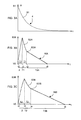
- FIG. 1 illustrates an example of a signal to be processed by a device or process according to embodiments of the invention
- FIG. 2 represents a first diagram of a device according to an embodiment of the invention
- FIGS. 3A, 3 B and 3 C represent signals in a device according to an embodiment of the invention
- FIG. 4 represents a second diagram of a device according to an embodiment of the invention.
- FIG. 5 represents a third diagram of a device according to an embodiment of the invention.
- FIG. 6 represents a first diagram of an electrical apparatus according to an embodiment of the invention.
- FIG. 7 represents a second diagram of an electrical apparatus according to an embodiment of the invention.
- FIG. 8 represents a processing process according to an embodiment of the invention.
- a signal S 1 represented in FIG. 1 comprises pulses 2 each having a rising first part 3 going from a minimum value up to a maximum amplitude value A and a second part 4 decreasing appreciably exponentially.
- a processing device When measurements or information carried by the signal 1 are in a time constant of the descent part 4 , a processing device enables a signal representative of said time constant to be supplied.
- A represents the amplitude of the signal
- t represents the time
- Ct represents the time constant of the signal on the descent
- Off represents an offset value able to be introduced in particular by an amplifier.
- the signal is preferably integrated during a preset time.
- the value of the time constant Ct can then be determined at the end of integration.
- the signal to be integrated is integrated in a first step in a first direction during a preset time and in a second opposite direction during appreciably the same time.
- a processing device 5 receives the signal S 1 to be measured and supplies a signal S 2 representative of a time constant on the descent of the signal S 1 .
- the signal S 1 is amplified by an amplifier 6 that supplies an amplified signal S 1 A.
- the signal S 1 A is applied to an inverter 7 to supply an inverted signal S 1 I.
- a first integrator 8 successively receives the signals S 1 A and S 1 I then supplies an integration signal S 3 to a control circuit 9 to extract the signal S 2 .
- the control circuit 9 commands a switch 10 to apply to the input of the first integrator the signal in a first direction S 1 A or the signal S 1 I that is in a second direction opposite to the first direction.
- the control circuit 9 also enables operation of the integrator to be commanded, in particular by initializing the integrator before each pulse of the signal S 1 .
- the amplifier When a signal S 1 is applied to the input of the processing device 5 , the amplifier amplifies the signal with the risk of superposing an offset signal Off on the amplified signal. Since in the equation F1(t) the signal Off is a constant, this signal is practically annulled by a first integration in a first direction and a second integration of the same duration in the opposite direction.
- F2 ⁇ ( t ) 1 RC ⁇ ( ⁇ t0 t0 + T1 ⁇ F1 ⁇ ( t ) ⁇ ⁇ ⁇ t - ⁇ t0 + T1 t0 + 2 ⁇ T1 ⁇ F1 ⁇ ( t ) ⁇ ⁇ ⁇ t ) ( 2 )
- a variable RC corresponds to an integration parameter, for example to a resistor and a capacitor associated to an operational amplifier in the case of an analog embodiment.
- a time t0 corresponds to the beginning of integration and T1 corresponds to the integration times in a first direction and in a second direction.
- two integrations of the signal over different time durations supply two integration signals respectively S 3 A and S 3 B.
- the integration times in one direction and then in the other are represented by a value T1
- the integration times in one direction and then in the other are represented by a value T2.
- the control device enables the value of the time constant Ct as a function of the ratio between the values of the integration signals S 3 A and S 3 B to be extracted.
- T2 corresponds to the integration times in a first direction and in a second direction, T2 being different from T1.
- F4 ⁇ ( Ct ) - 2 ⁇ ⁇ - t0 + T1 Ct + ⁇ - t0 Ct + ⁇ - t0 + 2 ⁇ T1 Ct - 2 ⁇ ⁇ - t0 + T2 Ct + ⁇ - t0 Ct + ⁇ - t0 + 2 ⁇ T2 Ct ( 6 )
- FIGS. 3A, 3 B and 3 C respectively illustrate the descending part of the signal S 1 or S 1 A and the integration signals S 3 A and S 3 B.
- the signal S 3 A represents integration of the signal S 1 or S 1 A in a first direction for a time T1 between a beginning of integration time t0 and a time t1. Then between the time t1 and a time t2, a second integration of the inverted signal S 1 or S 1 I takes place during a second time T1.
- These two successive integrations can be represented by a function F2(t) and a value IS 3 A of the signal S 3 A at the end of integration at the time t2 can be represented by a function F3(t) or F3a(t).
- the signal S 3 B represents integration of the signal S 1 or S 1 A in a first direction during a time T2 different from T1 between a beginning of integration time t0 and a time t3. Then, between the t3 and a time t4, a second integration of the inverted signal S 1 or S 1 I takes place during a second time T2.
- These two successive integrations can be represented by a function F2(t) in which T1 is replaced by T2 and a value IS 3 B of the signal S 3 B at the end of integration at the time t4 can be represented by a function F3b(t).
- Comparison of the signals IS 3 A and IS 3 B at the end of integration enables the influence of the amplitude A of the signal S 1 to be eliminated.
- measurement of the time constant Ct remains stable in time.
- Relations between the time constant Ct and the ratio of the signals IS 3 A and IS 3 B can be made according to the function F4(Ct). This relation can be made by calculation or by table of correspondence in a memory.
- FIG. 4 An embodiment of a processing device 5 with two integration circuits is represented in FIG. 4.
- a first integration circuit 8 A associated to a switch 10 A supplies the first signal S 3 A integrated with first times T1
- a second integration circuit 8 B associated to a switch 10 B supplies the second signal S 3 B integrated with second times T2.
- the control circuit 9 monitors the different integrations of the signal, receives the signals S 3 A and S 3 B, and supplies a signal S 2 representative of the time constant Ct of the input signal.
- the integrations are made with analog components with RC circuits introducing integration constants, it is possible to annul the effects of the precisions of these components by performing an integration of a reference signal Vref.
- the starting point of this integration corresponds to the values IS 3 A and IS 3 B of the signal(s) S 3 A and S 3 B at the end of integration at the times respectively t2 or t4.
- the end of integration corresponds to the time when the integration signal reaches a threshold value, preferably a nil value.
- the integration times represented respectively by T3A between the time t2 and a time t5, and by T3B between the time t4 and a time t6, are then directly representative of the values of said signals IS 3 A and IS 3 B.
- the integration constants RC introduced in all the integrations are annulled at the end of integration.
- the reference signal Vref can advantageously be proportional to the amplitude A of the signal S 1 .
- the time T3 is variable, it depends on an integration overshoot threshold, for example a threshold of zero value.
- Vref can be of positive or negative value according to the initial direction of S 1 .
- T3A A ⁇ Ct Vref ⁇ ( - 2 ⁇ ⁇ - t0 + T1 Ct + ⁇ - t0 Ct + ⁇ - t0 + 2 ⁇ T1 Ct )
- T3B A ⁇ Ct Vref ⁇ ( - 2 ⁇ ⁇ - t0 + T2 Ct + ⁇ - t0 Ct + ⁇ - t0 + 2 ⁇ T2 Ct ) ( 11 )
- the ratio of S 3 A over S 3 B corresponding to T3A /T3B can be expressed by the following function F4(Ct):
- F4 ⁇ ( Ct ) - 2 ⁇ ⁇ - t0 + T1 Ct + ⁇ - t0 Ct + ⁇ - t0 + 2 ⁇ T1 Ct - 2 ⁇ ⁇ - t0 + T2 Ct + ⁇ - t0 Ct + ⁇ - t0 + 2 ⁇ T2 Ct ( 12 )
- FIG. 5 shows an embodiment wherein integrators 8 A and 8 B are achieved in analog manner.
- Each integrator comprises an amplifier 11 A and 11 B respectively associated to an input resistor 12 A and 12 B and a capacitor 13 A and 13 B.
- the input resistors of the integrators are connected to switches respectively 10 A and 10 B to receive the signals S 1 A, S 1 I and a reference signal Vref supplied by a reference voltage source 14 .
- the switches are commanded during different time durations.
- the switch 10 A is commanded by a synchronization and counting circuit 36 of the control circuit 9 to apply the signal S 1 A during a time T1, then the signal S 1 I during a time T1, and finally the signal Vref to the input resistor 12 A of the integrator 8 A to make the integrator integrate up to a nil value V0 of the integration output.
- the control circuit 9 comprises means 36 for counting the integration time up to a nil value V0 of the output of the integrator 8 A.
- a comparator 15 A connected to the integrator 8 A, detects the zero crossing V0 of the integration output and informs the circuit 36 of the control circuit 9 to stop counting of the integration time T3A.
- the switch 10 B is commanded by the circuit 36 to apply the signal S 1 A during a time T2, then the signal S 1 I during a time T2 and finally the signal Vref to the input resistor 12 B of the integrator 8 B to make the integrator integrate up to a nil value V0 of the integration output.
- the control circuit 9 comprises means 36 for counting the integration time up to a nil value V0 of the output of the integrator 8 B.
- a comparator 15 B connected to the integrator 8 B, detects the zero crossing V0 of the integration output and informs the circuit 36 of the control circuit 9 to stop counting of the integration time T3B.
- the integrations of the reference value Vref are represented in parts 16 A and 16 B of the curves of FIGS. 3B and 3C. These final integrations eliminate the influence of the precision of the integrator components, in particular the resistors 12 A and 12 B and capacitors 13 A and 13 B.
- the use, in each integrator, of appreciably equal integration periods while inverting the input signal enables the effects of an offset signal Off to be cancelled out.
- the integrators are initialized by the control circuit which sets the inputs to a zero value corresponding to the ground of the circuit and discharges the capacitors 13 A and 13 B by commanding discharge devices 17 A and 17 B.
- the signal S 2 representative of the time constant on the descent of the input signal S 1 can be determined in the control circuit as a function of the times T3A and T3B or of the ratio T3A/T3B between said times representative of the ratio S 3 A/S 3 B determined in a circuit 37.
- the value Ct of S 2 can advantageously be supplied by means of a table 38 of correspondence receiving the values of the rations T3A/T3B or S 3 A/S 3 B. This table is preferably stored notably in an electronic memory.
- the use of two integration channels having different integration times T1 and T2 eliminates the influence of the value of the amplitude of the input signal.
- the integration circuits 8 A and 8 B can comprise capacitors and resistors that are precisely adjusted, in particular by screen-printing, by laser or sand jet cutting. These circuits enable the control circuit 9 to be advantageously simplified and integration with a reference value Vref represented by the parts of curves 16 A and 16 B to be avoided.
- means for receiving a light signal 18 are connected to the amplifier 6 .
- These means for receiving a light signal can receive light signals supplied by a sensor with fluorescent or luminescent material having an appreciably exponential decrease after excitation by light rays.
- the exponential decrease of the light signal supplied by the sensor with fluorescent or luminescent material can be representative of a temperature to be measured.
- An electrical apparatus comprises an electrical conductor 20 on which conductor a sensor 21 with fluorescent or luminescent material 22 is arranged.
- the sensor 21 comprises, for example, two optic carriers such as optic fibers 23 and 24 to direct a first excitation light beam 25 to the material 22 and to retrieve a second light beam 26 coming from the material 22 and directed to the means for receiving 18 .
- the first beam can be emitted by an emitting circuit 27 synchronized for example with the processing device 5 .
- the signal of the second beam comes from the material 22 which reacts to the excitation of the first beam.
- the reaction of the material 22 is dependent on the temperature which modifies the time constant on the descent of the signal.
- the arrangement of such a material 22 on an electrical conductor 20 enables the temperature or heat rise thereof when an electric current is flowing therethrough to be measured.
- the fluorescent or luminescent material of the sensor is preferably arranged on a part 28 of the conductor having the form of an electric shunt.
- FIG. 7 represents an electrical apparatus comprising at least one electrical contact 29 connected in series with at least one electrical conductor 20 .
- a sensor 21 is arranged on a part 28 of the conductor having the form of a shunt to supply a signal S 1 the part of decreasing exponential form of which signal is representative of the temperature detected by the sensor.
- the sensor can detect the temperature of the conductor in the part in the form of an electric shunt liable to heat by flow of an electric current.
- a processing device 5 is connected to the sensor 21 to receive the signal S 1 and to supply an output signal S 2 representative of the time constant of the pulses of the signal S 1 and consequently representative of the temperature of the conductor 20 and of the current flowing therethrough.
- a tripping function processing circuit 30 is connected on output of the processing device 5 to receive the signal S 2 .
- the circuit 30 processes the tripping functions and supplies a tripping order to a trip relay 31 to cause opening of the contact 29 by a mechanism 32 . For example, if the signal S 2 exceeds a preset threshold, instantaneously or for a preset time, the processing circuit 30 gives a tripping order to open said at least one contact 29 .
- FIG. 8 A flowchart of a processing process is represented in FIG. 8 .
- This signal processing process comprises a determining phase to supply a value representative of a time constant of a part of an input signal S 1 or S 1 A having an appreciably exponential form.
- Said determining phase comprises a first step of integration 40 of the input signal S 1 or S 1 A in a first direction during a first preset time T1 beginning at a time t0, and a second step 41 of integration of the input signal S 1 or S 1 I in a second direction opposite from the first direction during a second preset time T1 appreciably equal to the first time and succeeding said first time.
- an extraction step 44 supplies a value S 2 or Ct representative of the time constant as a function of a signal S 3 A integrated by the integration steps 40 and 41 .
- the process comprises two integration channels to eliminate the influence of the amplitude of the signal S 1 .
- the determining phase comprises a third integration step 42 of the input signal S 1 or S 1 A in a first direction during a third preset time T2 different from the first time T1 and beginning appreciably at the same time t0 as said first step 40 , and a fourth integration step 43 of the input signal S 1 or in a second direction opposite from the first direction during a fourth preset time T2 appreciably equal to the third time and succeeding said third step.
- the extraction step supplies the value S 2 or Ct representative of a time constant as a function of a signal S 3 A integrated by the first and second integration steps 40 and 41 , and of a signal S 3 B integrated by the third and fourth integration steps 42 and 43 .
- the extraction step 44 supplies the value S 2 or Ct representative of a time constant as a function of the ratio S 3 A/S 3 B or S 3 B/S 3 A between the signal S 3 A integrated by the first and second integration step and the signal S 3 B integrated by the third and fourth integration step.
- the device and process described above can be implemented in embodiments comprising in particular analog, digital and/or programmed components in a microcontroller or for a microprocessor.
Landscapes
- Physics & Mathematics (AREA)
- General Physics & Mathematics (AREA)
- Indication And Recording Devices For Special Purposes And Tariff Metering Devices (AREA)
- Breakers (AREA)
- Photometry And Measurement Of Optical Pulse Characteristics (AREA)
- Measurement Of Current Or Voltage (AREA)
- Manipulation Of Pulses (AREA)
Applications Claiming Priority (2)
| Application Number | Priority Date | Filing Date | Title |
|---|---|---|---|
| FR0016915A FR2818830B1 (fr) | 2000-12-22 | 2000-12-22 | Dispositif et procede de traitement de signal et appareil electrique comportant un tel dispositif |
| FR0016915 | 2000-12-22 |
Publications (2)
| Publication Number | Publication Date |
|---|---|
| US20020118129A1 US20020118129A1 (en) | 2002-08-29 |
| US6549033B2 true US6549033B2 (en) | 2003-04-15 |
Family
ID=8858107
Family Applications (1)
| Application Number | Title | Priority Date | Filing Date |
|---|---|---|---|
| US10/011,728 Expired - Lifetime US6549033B2 (en) | 2000-12-22 | 2001-12-11 | Signal processing device and process and electrical apparatus comprising such a device |
Country Status (4)
| Country | Link |
|---|---|
| US (1) | US6549033B2 (fr) |
| EP (1) | EP1223417A1 (fr) |
| JP (1) | JP4212807B2 (fr) |
| FR (1) | FR2818830B1 (fr) |
Families Citing this family (2)
| Publication number | Priority date | Publication date | Assignee | Title |
|---|---|---|---|---|
| US9602118B2 (en) | 2015-08-07 | 2017-03-21 | Texas Instruments Incorporated | Amplifier sharing technique for power reduction in analog-to-digital converter |
| JP2022507037A (ja) * | 2018-11-14 | 2022-01-18 | 11093568 カナダ エルティーディー. | 高分解能多重化システム |
Citations (6)
| Publication number | Priority date | Publication date | Assignee | Title |
|---|---|---|---|---|
| US5043585A (en) | 1990-01-03 | 1991-08-27 | Degussa Aktiengesellschaft | Method and apparatus for measurement of the fluorescence relaxation period of a fluorescent substance |
| WO1992007240A1 (fr) | 1990-10-18 | 1992-04-30 | Rosemount Inc. | Capteur de temperature par mesure de vitesse temporelle de declin de luminescence et systeme electronique |
| US5255980A (en) | 1990-10-18 | 1993-10-26 | Rosemount Inc. | Black body TRD temperature sensor |
| US5600147A (en) * | 1993-06-11 | 1997-02-04 | Luxtron Corporation | Temperature measuring system having improved signal processing and multiple optical sensors |
| EP0940655A1 (fr) | 1998-03-06 | 1999-09-08 | Schneider Electric Industries SA | Sonde de mesure comportant au moins une fibre optique, dispositif de mesure et installation comportant au moins une telle sonde |
| US5986272A (en) * | 1997-11-10 | 1999-11-16 | American Iron And Steel Institute | Real-time method and apparatus for measuring the temperature of a fluorescing phosphor |
-
2000
- 2000-12-22 FR FR0016915A patent/FR2818830B1/fr not_active Expired - Fee Related
-
2001
- 2001-09-27 EP EP01410123A patent/EP1223417A1/fr not_active Withdrawn
- 2001-12-11 US US10/011,728 patent/US6549033B2/en not_active Expired - Lifetime
- 2001-12-20 JP JP2001388118A patent/JP4212807B2/ja not_active Expired - Fee Related
Patent Citations (7)
| Publication number | Priority date | Publication date | Assignee | Title |
|---|---|---|---|---|
| US5043585A (en) | 1990-01-03 | 1991-08-27 | Degussa Aktiengesellschaft | Method and apparatus for measurement of the fluorescence relaxation period of a fluorescent substance |
| WO1992007240A1 (fr) | 1990-10-18 | 1992-04-30 | Rosemount Inc. | Capteur de temperature par mesure de vitesse temporelle de declin de luminescence et systeme electronique |
| US5255980A (en) | 1990-10-18 | 1993-10-26 | Rosemount Inc. | Black body TRD temperature sensor |
| US5600147A (en) * | 1993-06-11 | 1997-02-04 | Luxtron Corporation | Temperature measuring system having improved signal processing and multiple optical sensors |
| US5986272A (en) * | 1997-11-10 | 1999-11-16 | American Iron And Steel Institute | Real-time method and apparatus for measuring the temperature of a fluorescing phosphor |
| EP0940655A1 (fr) | 1998-03-06 | 1999-09-08 | Schneider Electric Industries SA | Sonde de mesure comportant au moins une fibre optique, dispositif de mesure et installation comportant au moins une telle sonde |
| US6204915B1 (en) | 1998-03-06 | 2001-03-20 | Schneider Electric Sa | Measuring probe comprising at least one optic fiber, and a measuring device and installation comprising at least one such probe |
Also Published As
| Publication number | Publication date |
|---|---|
| EP1223417A1 (fr) | 2002-07-17 |
| FR2818830B1 (fr) | 2003-02-07 |
| JP4212807B2 (ja) | 2009-01-21 |
| FR2818830A1 (fr) | 2002-06-28 |
| US20020118129A1 (en) | 2002-08-29 |
| JP2002303534A (ja) | 2002-10-18 |
Similar Documents
| Publication | Publication Date | Title |
|---|---|---|
| US11125863B2 (en) | Correction device, correction method, and distance measuring device | |
| GB997198A (en) | Adaptive recognition method and system | |
| KR940015737A (ko) | 전류제한 솔레노이드 드라이버 | |
| EP3596824B1 (fr) | Amplificateur | |
| US5008695A (en) | Rangefinder for camera | |
| US6549033B2 (en) | Signal processing device and process and electrical apparatus comprising such a device | |
| WO1999053425A1 (fr) | Appareil et technique permettant d'ameliorer la plage dynamique et le temps de reponse d'un amplificateur logarithmique | |
| CN104458034A (zh) | 温度检测方法和温度检测装置 | |
| US9746865B2 (en) | Current-to-voltage conversion circuit, reception apparatus, and imaging system | |
| KR870000597A (ko) | 저 저항 측정 저항계 및 방법 | |
| HU196513B (en) | Apparatus for measuring voltage by sampling | |
| JP2002525581A (ja) | 電荷流を周波数信号に変換する装置及び方法 | |
| CN105359251A (zh) | 质量分析装置和质量分析装置的控制方法 | |
| EP2990826B1 (fr) | Agencement de circuit d'attaque optique et procédé pour générer un signal d'attaque | |
| US3016488A (en) | Automatic range selector | |
| JPS60169740A (ja) | 煙検出装置 | |
| US3571706A (en) | Voltage measuring apparatus employing feedback gain control to obtain a predetermined output and a feedback loop to readout the gain value | |
| US3349251A (en) | Level sensor circuit | |
| HU187978B (en) | Method and circuit arrangement for measuring light at least in a range of six order of magnitude, preferably for tld apparatuses | |
| SU1597964A1 (ru) | Источник ионов с поверхностной ионизацией | |
| JP2791550B2 (ja) | 光受信回路 | |
| SU894614A1 (ru) | Устройство дл задани и измерени пикового тока туннельных диодов | |
| US6134943A (en) | Electron capture detector for gas chromatograph | |
| GB2224570A (en) | Measuring the flash duration of a flash gun | |
| US20190128748A1 (en) | Current-based temperature measurement devices and methods |
Legal Events
| Date | Code | Title | Description |
|---|---|---|---|
| AS | Assignment |
Owner name: SCHNEIDER ELECTRIC INDUSTRIES SA, FRANCE Free format text: ASSIGNMENT OF ASSIGNORS INTEREST;ASSIGNORS:MOUSSANET, ROLAND;PERICHON, PIERRE;REEL/FRAME:012373/0291 Effective date: 20011114 |
|
| FEPP | Fee payment procedure |
Free format text: PAYOR NUMBER ASSIGNED (ORIGINAL EVENT CODE: ASPN); ENTITY STATUS OF PATENT OWNER: LARGE ENTITY |
|
| STCF | Information on status: patent grant |
Free format text: PATENTED CASE |
|
| FPAY | Fee payment |
Year of fee payment: 4 |
|
| FPAY | Fee payment |
Year of fee payment: 8 |
|
| FPAY | Fee payment |
Year of fee payment: 12 |