US6509238B1 - Method for manufacturing a MOS device with improved well control stability - Google Patents
Method for manufacturing a MOS device with improved well control stability Download PDFInfo
- Publication number
- US6509238B1 US6509238B1 US10/100,676 US10067602A US6509238B1 US 6509238 B1 US6509238 B1 US 6509238B1 US 10067602 A US10067602 A US 10067602A US 6509238 B1 US6509238 B1 US 6509238B1
- Authority
- US
- United States
- Prior art keywords
- gate
- semiconductor substrate
- recited
- conducting
- forming
- Prior art date
- Legal status (The legal status is an assumption and is not a legal conclusion. Google has not performed a legal analysis and makes no representation as to the accuracy of the status listed.)
- Expired - Lifetime
Links
Images


Classifications
-
- H—ELECTRICITY
- H10—SEMICONDUCTOR DEVICES; ELECTRIC SOLID-STATE DEVICES NOT OTHERWISE PROVIDED FOR
- H10D—INORGANIC ELECTRIC SEMICONDUCTOR DEVICES
- H10D64/00—Electrodes of devices having potential barriers
- H10D64/01—Manufacture or treatment
- H10D64/015—Manufacture or treatment removing at least parts of gate spacers, e.g. disposable spacers
-
- H—ELECTRICITY
- H10—SEMICONDUCTOR DEVICES; ELECTRIC SOLID-STATE DEVICES NOT OTHERWISE PROVIDED FOR
- H10D—INORGANIC ELECTRIC SEMICONDUCTOR DEVICES
- H10D30/00—Field-effect transistors [FET]
- H10D30/01—Manufacture or treatment
- H10D30/021—Manufacture or treatment of FETs having insulated gates [IGFET]
- H10D30/0223—Manufacture or treatment of FETs having insulated gates [IGFET] having source and drain regions or source and drain extensions self-aligned to sides of the gate
- H10D30/0227—Manufacture or treatment of FETs having insulated gates [IGFET] having source and drain regions or source and drain extensions self-aligned to sides of the gate having both lightly-doped source and drain extensions and source and drain regions self-aligned to the sides of the gate, e.g. lightly-doped drain [LDD] MOSFET or double-diffused drain [DDD] MOSFET
-
- H—ELECTRICITY
- H10—SEMICONDUCTOR DEVICES; ELECTRIC SOLID-STATE DEVICES NOT OTHERWISE PROVIDED FOR
- H10D—INORGANIC ELECTRIC SEMICONDUCTOR DEVICES
- H10D64/00—Electrodes of devices having potential barriers
- H10D64/01—Manufacture or treatment
- H10D64/021—Manufacture or treatment using multiple gate spacer layers, e.g. bilayered sidewall spacers
-
- H—ELECTRICITY
- H10—SEMICONDUCTOR DEVICES; ELECTRIC SOLID-STATE DEVICES NOT OTHERWISE PROVIDED FOR
- H10P—GENERIC PROCESSES OR APPARATUS FOR THE MANUFACTURE OR TREATMENT OF DEVICES COVERED BY CLASS H10
- H10P74/00—Testing or measuring during manufacture or treatment of wafers, substrates or devices
- H10P74/23—Testing or measuring during manufacture or treatment of wafers, substrates or devices characterised by multiple measurements, corrections, marking or sorting processes
Definitions
- the present invention relates to semiconductor devices and, more particularly, to a method for manufacturing a MOS (referred to as MOS hereafter) device with improved well control stability.
- MOS referred to as MOS hereafter
- Offset spacers are used in semiconductor devices.
- the Offset spacers can benefit the process window of photolithography and allow the realization of smaller cell size and therefore smaller chip size.
- FIGS. 1A through 1C illustrate, in cross-section, the conventional offset spacers process.
- This process begins by providing a semiconductor substrate 10 having a gate electrode 12 .
- the gate electrode 12 includes a gate oxide layer 14 and a conducting gate 16 as shown in FIG. 1 A.
- the conducting gate 16 is typically a polysilicon (poly) gate.
- offset spacers 18 are formed on sidewalls of the gate electrode 14 .
- the offset spacers 18 typically have a fixed width, such as 150 angstroms.
- source and drain extensions 20 are formed in the semiconductor substrate 10 by ion implantation.
- Spacers 22 are formed on sidewalls of the gate electrode 12 .
- Source and drain regions 24 are formed in the semiconductor substrate 10 by ion implantation.
- the channel length of the device is fixed after poly etching and the critical dimension of the poly gate is not easily controlled by the patterning process beyond 0.13 ⁇ m.
- the critical dimension of the poly gate is not precise, electric characteristics are unstable and can not be remedied. Thus, the minimization of the feature size can not be achieved.
- An object according to the present invention is to provide a method for manufacturing a MOS device with improved well control stability characterized by improvement of electric characteristics of the device.
- the present invention achieves the above-indicated object by providing a method for determining conducting gate spacer thickness to well control MOS device stability comprising the steps of: providing a semiconductor substrate; forming a gate electrode according to a critical dimension on the semiconductor substrate, wherein the gate electrode comprises a gate oxide layer and a conducting gate; inspecting a real dimension of the conducting gate; determining a thickness of subsequently formed conducting gate spacers according to the real dimension of the conducting gate, such that variations of electric characteristics of the device affected by the critical dimension of the conducting gate are reduced; and forming the conducting gate spacers with the determined thickness on sidewalls of the gate electrode.
- FIGS. 1A through 1C Prior Art
- FIGS. 1A through 1C illustrate, in cross-section, the conventional offset spacers process
- FIG. 2 illustrates the Ids (current of source/drain) for various poly CDs (critical dimensions).
- FIGS. 3A through 3H illustrate, in cross-section, the process in accordance with the present invention.
- the Ids (current of source/drain) of nMOS can be adjusted through compensating various widths of the offset spacers, as shown in FIG. 2 .
- the poly (polysilicon) gates with different Ids' are attributed to various critical dimensions after etching inspection (AEI CD).
- AEI CD 0.092 to 0.097 ⁇ m
- offset spacers of 170 angstroms are used to compensate poly gates, as shown in FIG. 2, indicating that the Ids' are adjusted to 520 to 580 ⁇ A/ ⁇ m, as depicted in region R 20 .
- offset spacers of 160 angstroms are used to compensate poly gates, indicating that the Ids' are adjusted to 520 to 580 ⁇ A/ ⁇ m, as depicted in region R 22 .
- offset spacers of 150 angstroms are used to compensate poly gates, indicating that the Ids' are adjusted to 520 to 580 ⁇ A/ ⁇ m, as depicted in region R 24 .
- offset spacers of 140 angstroms are used to compensate poly gates, indicating that the Ids' are adjusted to 520 to 580 ⁇ A/ ⁇ m, as depicted in region R 26 .
- offset spacers of 130 angstroms are used to compensate poly gates, indicating that the Ids' are adjusted to 520 to 580 ⁇ A/ ⁇ m, as depicted in region R 28 .
- the present invention discloses a method for determining conducting gate spacer thickness to well control MOS device stability.
- this embodiment begins by providing a semiconductor substrate 100 .
- a gate electrode 102 is formed according to a critical dimension on the semiconductor substrate.
- the gate electrode 102 includes a gate oxide layer 104 and a conducting gate 106 .
- the gate oxide layer 104 is preferably formed of silicon oxide.
- the conducting gate 106 is preferably formed of polysilicon.
- a real dimension 108 of the conducting gate 106 is inspected.
- the electric characteristics of the device can be adjusted through compensating various widths of the offset spacers.
- a thickness of subsequently formed conducting gate spacers, for example poly spacers, according to the real dimension 108 of the conducting gate 106 is determined, such that variations of electric characteristics of the device affected by the critical dimension of the conducting gate 106 are reduced.
- the conducting gate spacers 110 with the determined thickness are formed on sidewalls of the gate electrode 102 .
- a thinner gate electrode 120 including a gate oxide layer 122 and a conducting gate 124 as shown in FIG. 3D
- conducting gate spacers 126 are formed on sidewalls of the gate electrode 120 as shown in FIG. 3 E.
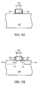
- a thicker gate electrode 130 including a gate oxide layer 132 and a conducting gate 134 as shown in FIG. 3F
- conducting gate spacers 136 are formed on sidewalls of the gate electrode 130 , as shown in FIG. 3 G.
- the conducting gate spacers 110 , 126 and 136 are preferably formed of SiO 2 , SiON or Si 3 N 4 .
- the conducting gate spacers 110 can be formed by the following steps. First, a dielectric layer (not shown) is formed on the semiconductor substrate 100 and the conducting gate 102 . The dielectric layer is also preferably formed of SiO 2 , SiON or Si 3 N 4 . Next, a portion of the dielectric layer on the semiconductor substrate 100 is removed, such that the conducting gate spacers 110 are formed.
- source and drain extensions 112 are formed in the semiconductor substrate 100 by ion implantation.
- Spacers 114 are formed on sidewalls of the gate electrode 102 .
- Source and drain regions 116 are formed in the semiconductor substrate 100 by ion implantation.
- the present invention provides a method for determining conducting gate spacer thickness that is real-time adjustable to well control MOS device stability and improve the electric characteristics of the device.
Landscapes
- Insulated Gate Type Field-Effect Transistor (AREA)
Abstract
Description
Claims (18)
Priority Applications (1)
| Application Number | Priority Date | Filing Date | Title |
|---|---|---|---|
| US10/100,676 US6509238B1 (en) | 2002-03-18 | 2002-03-18 | Method for manufacturing a MOS device with improved well control stability |
Applications Claiming Priority (1)
| Application Number | Priority Date | Filing Date | Title |
|---|---|---|---|
| US10/100,676 US6509238B1 (en) | 2002-03-18 | 2002-03-18 | Method for manufacturing a MOS device with improved well control stability |
Publications (1)
| Publication Number | Publication Date |
|---|---|
| US6509238B1 true US6509238B1 (en) | 2003-01-21 |
Family
ID=22280963
Family Applications (1)
| Application Number | Title | Priority Date | Filing Date |
|---|---|---|---|
| US10/100,676 Expired - Lifetime US6509238B1 (en) | 2002-03-18 | 2002-03-18 | Method for manufacturing a MOS device with improved well control stability |
Country Status (1)
| Country | Link |
|---|---|
| US (1) | US6509238B1 (en) |
Cited By (2)
| Publication number | Priority date | Publication date | Assignee | Title |
|---|---|---|---|---|
| WO2004044974A3 (en) * | 2002-11-12 | 2004-06-17 | Applied Materials Inc | Method and apparatus employing integrated metrology for improved dielectric etch efficiency |
| CN110112070A (en) * | 2019-04-28 | 2019-08-09 | 上海华虹宏力半导体制造有限公司 | MOS transistor and method of forming the same |
Citations (5)
| Publication number | Priority date | Publication date | Assignee | Title |
|---|---|---|---|---|
| US6136616A (en) * | 1998-02-11 | 2000-10-24 | Advanced Micro Devices | Method of forming semiconductor devices using gate electrode dimensions and dopant concentration for controlling drive current strength |
| US6187645B1 (en) * | 1999-01-19 | 2001-02-13 | United Microelectronics Corp. | Method for manufacturing semiconductor device capable of preventing gate-to-drain capacitance and eliminating birds beak formation |
| US6294432B1 (en) * | 1999-12-20 | 2001-09-25 | United Microelectronics Corp. | Super halo implant combined with offset spacer process |
| US20020090771A1 (en) * | 2000-10-26 | 2002-07-11 | Yung-Chang Lin | Self-align offset gate structure and method of manufacture |
| US20020132377A1 (en) * | 2001-03-19 | 2002-09-19 | International Business Machines Corporation | Effective channel length control using ion implant feed forward |
-
2002
- 2002-03-18 US US10/100,676 patent/US6509238B1/en not_active Expired - Lifetime
Patent Citations (5)
| Publication number | Priority date | Publication date | Assignee | Title |
|---|---|---|---|---|
| US6136616A (en) * | 1998-02-11 | 2000-10-24 | Advanced Micro Devices | Method of forming semiconductor devices using gate electrode dimensions and dopant concentration for controlling drive current strength |
| US6187645B1 (en) * | 1999-01-19 | 2001-02-13 | United Microelectronics Corp. | Method for manufacturing semiconductor device capable of preventing gate-to-drain capacitance and eliminating birds beak formation |
| US6294432B1 (en) * | 1999-12-20 | 2001-09-25 | United Microelectronics Corp. | Super halo implant combined with offset spacer process |
| US20020090771A1 (en) * | 2000-10-26 | 2002-07-11 | Yung-Chang Lin | Self-align offset gate structure and method of manufacture |
| US20020132377A1 (en) * | 2001-03-19 | 2002-09-19 | International Business Machines Corporation | Effective channel length control using ion implant feed forward |
Cited By (2)
| Publication number | Priority date | Publication date | Assignee | Title |
|---|---|---|---|---|
| WO2004044974A3 (en) * | 2002-11-12 | 2004-06-17 | Applied Materials Inc | Method and apparatus employing integrated metrology for improved dielectric etch efficiency |
| CN110112070A (en) * | 2019-04-28 | 2019-08-09 | 上海华虹宏力半导体制造有限公司 | MOS transistor and method of forming the same |
Similar Documents
| Publication | Publication Date | Title |
|---|---|---|
| US6798027B2 (en) | Semiconductor device including gate insulation films having different thicknesses | |
| US5863824A (en) | Method of forming semiconductor devices using gate electrode length and spacer width for controlling drivecurrent strength | |
| US7396713B2 (en) | Structure and method for forming asymmetrical overlap capacitance in field effect transistors | |
| US5166087A (en) | Method of fabricating semiconductor element having lightly doped drain (ldd) without using sidewalls | |
| CN101375381B (en) | Method of forming a field effect transistor and method of forming an integrated circuit comprising a gate array of transistors and circuitry surrounding said gate array | |
| US5424234A (en) | Method of making oxide semiconductor field effect transistor | |
| US20080138956A1 (en) | Manufacturing method of semiconductor device | |
| JP4255235B2 (en) | Method for manufacturing gate dielectric | |
| US5891783A (en) | Method of reducing fringe capacitance | |
| US20060063316A1 (en) | Method for fabricating semiconductor device | |
| US6344397B1 (en) | Semiconductor device having a gate electrode with enhanced electrical characteristics | |
| US5527725A (en) | Method for fabricating a metal oxide semiconductor field effect transistor | |
| US6509238B1 (en) | Method for manufacturing a MOS device with improved well control stability | |
| US20100308382A1 (en) | Semiconductor structures and methods for reducing silicon oxide undercuts in a semiconductor substrate | |
| US6255182B1 (en) | Method of forming a gate structure of a transistor by means of scalable spacer technology | |
| US6228663B1 (en) | Method of forming semiconductor devices using gate insulator thickness and channel length for controlling drive current strength | |
| KR20010004237A (en) | A method for forming semiconductor memory device including self-aligned contact process | |
| JPH02196434A (en) | Manufacture of mos transistor | |
| US6670252B2 (en) | Method of manufacturing semiconductor device | |
| JPH01251668A (en) | Manufacture of field effect transistor | |
| KR20100074479A (en) | Semiconductor device and method for manufacturing the same | |
| JPH1012871A (en) | Method for manufacturing semiconductor device | |
| US6936517B2 (en) | Method for fabricating transistor of semiconductor device | |
| KR100477542B1 (en) | Method of manufacturing short-channel transistor in semiconductor device | |
| KR20020096393A (en) | Method for Fabricating MOS transistor |
Legal Events
| Date | Code | Title | Description |
|---|---|---|---|
| AS | Assignment |
Owner name: SILICON INTEGRATED SYSTEMS CORP., TAIWAN Free format text: ASSIGNMENT OF ASSIGNORS INTEREST;ASSIGNORS:WANG, TENG-FENG;CHEN, LUNG;HSUE, CHEN-CHIU;REEL/FRAME:012710/0869;SIGNING DATES FROM 20020220 TO 20020221 |
|
| STCF | Information on status: patent grant |
Free format text: PATENTED CASE |
|
| AS | Assignment |
Owner name: UNITED MICROELECTRONICS CORP., TAIWAN Free format text: ASSIGNMENT OF ASSIGNORS INTEREST;ASSIGNOR:SILICON INTEGRATED SYSTEMS CORP.;REEL/FRAME:015621/0932 Effective date: 20050126 |
|
| FPAY | Fee payment |
Year of fee payment: 4 |
|
| FPAY | Fee payment |
Year of fee payment: 8 |
|
| FPAY | Fee payment |
Year of fee payment: 12 |