US6506641B1 - Use of selective oxidation to improve LDMOS power transistors - Google Patents
Use of selective oxidation to improve LDMOS power transistors Download PDFInfo
- Publication number
- US6506641B1 US6506641B1 US09/641,086 US64108600A US6506641B1 US 6506641 B1 US6506641 B1 US 6506641B1 US 64108600 A US64108600 A US 64108600A US 6506641 B1 US6506641 B1 US 6506641B1
- Authority
- US
- United States
- Prior art keywords
- oxide
- gate electrode
- gate
- tapered
- less
- Prior art date
- Legal status (The legal status is an assumption and is not a legal conclusion. Google has not performed a legal analysis and makes no representation as to the accuracy of the status listed.)
- Expired - Lifetime
Links
Images

Classifications
-
- H—ELECTRICITY
- H10—SEMICONDUCTOR DEVICES; ELECTRIC SOLID-STATE DEVICES NOT OTHERWISE PROVIDED FOR
- H10D—INORGANIC ELECTRIC SEMICONDUCTOR DEVICES
- H10D30/00—Field-effect transistors [FET]
- H10D30/60—Insulated-gate field-effect transistors [IGFET]
- H10D30/64—Double-diffused metal-oxide semiconductor [DMOS] FETs
- H10D30/65—Lateral DMOS [LDMOS] FETs
-
- H—ELECTRICITY
- H10—SEMICONDUCTOR DEVICES; ELECTRIC SOLID-STATE DEVICES NOT OTHERWISE PROVIDED FOR
- H10W—GENERIC PACKAGES, INTERCONNECTIONS, CONNECTORS OR OTHER CONSTRUCTIONAL DETAILS OF DEVICES COVERED BY CLASS H10
- H10W10/00—Isolation regions in semiconductor bodies between components of integrated devices
- H10W10/01—Manufacture or treatment
- H10W10/011—Manufacture or treatment of isolation regions comprising dielectric materials
- H10W10/012—Manufacture or treatment of isolation regions comprising dielectric materials using local oxidation of silicon [LOCOS]
-
- H—ELECTRICITY
- H10—SEMICONDUCTOR DEVICES; ELECTRIC SOLID-STATE DEVICES NOT OTHERWISE PROVIDED FOR
- H10W—GENERIC PACKAGES, INTERCONNECTIONS, CONNECTORS OR OTHER CONSTRUCTIONAL DETAILS OF DEVICES COVERED BY CLASS H10
- H10W10/00—Isolation regions in semiconductor bodies between components of integrated devices
- H10W10/10—Isolation regions comprising dielectric materials
- H10W10/13—Isolation regions comprising dielectric materials formed using local oxidation of silicon [LOCOS], e.g. sealed interface localised oxidation [SILO] or side-wall mask isolation [SWAMI]
-
- H—ELECTRICITY
- H10—SEMICONDUCTOR DEVICES; ELECTRIC SOLID-STATE DEVICES NOT OTHERWISE PROVIDED FOR
- H10D—INORGANIC ELECTRIC SEMICONDUCTOR DEVICES
- H10D62/00—Semiconductor bodies, or regions thereof, of devices having potential barriers
- H10D62/10—Shapes, relative sizes or dispositions of the regions of the semiconductor bodies; Shapes of the semiconductor bodies
- H10D62/13—Semiconductor regions connected to electrodes carrying current to be rectified, amplified or switched, e.g. source or drain regions
- H10D62/149—Source or drain regions of field-effect devices
- H10D62/151—Source or drain regions of field-effect devices of IGFETs
- H10D62/156—Drain regions of DMOS transistors
- H10D62/157—Impurity concentrations or distributions
-
- H—ELECTRICITY
- H10—SEMICONDUCTOR DEVICES; ELECTRIC SOLID-STATE DEVICES NOT OTHERWISE PROVIDED FOR
- H10D—INORGANIC ELECTRIC SEMICONDUCTOR DEVICES
- H10D64/00—Electrodes of devices having potential barriers
- H10D64/20—Electrodes characterised by their shapes, relative sizes or dispositions
- H10D64/27—Electrodes not carrying the current to be rectified, amplified, oscillated or switched, e.g. gates
- H10D64/311—Gate electrodes for field-effect devices
- H10D64/411—Gate electrodes for field-effect devices for FETs
- H10D64/511—Gate electrodes for field-effect devices for FETs for IGFETs
- H10D64/514—Gate electrodes for field-effect devices for FETs for IGFETs characterised by the insulating layers
- H10D64/516—Gate electrodes for field-effect devices for FETs for IGFETs characterised by the insulating layers the thicknesses being non-uniform
-
- H—ELECTRICITY
- H10—SEMICONDUCTOR DEVICES; ELECTRIC SOLID-STATE DEVICES NOT OTHERWISE PROVIDED FOR
- H10P—GENERIC PROCESSES OR APPARATUS FOR THE MANUFACTURE OR TREATMENT OF DEVICES COVERED BY CLASS H10
- H10P14/00—Formation of materials, e.g. in the shape of layers or pillars
- H10P14/60—Formation of materials, e.g. in the shape of layers or pillars of insulating materials
- H10P14/61—Formation of materials, e.g. in the shape of layers or pillars of insulating materials using masks
Definitions
- This invention relates to laterally diffused metal oxide semiconductor (LDMOS) transistors.
- LDMOS laterally diffused metal oxide semiconductor
- LDMOS Lateral Diffused Metal Oxide Semiconductor devices
- the operation is often constrained in frequency by the gate to drain overlap capacitance as well as reliability issues that relate to the electric field in the vicinity of the drain and its effect on “hot carrier aging.”
- Past attempts to minimize these problems deviate from using a gate oxide of uniform thickness by placing one edge of the gate over a region of thicker oxide (thicker than gate oxide) as shown in prior art FIGS. 1 and 2.
- this thicker oxide is grown first and the gate is then aligned to the thicker oxide. This results in uncertain device characteristics due to the vagaries of the alignment and shape of the transition region between the thick and thin oxide regions.
- FIGS. 1 & 2 There are several disadvantages to using a uniform gate oxide thickness and the prior art structures of FIGS. 1 & 2 :
- the gate oxide thickness significantly determines the threshold voltage of the device and the maximum gate voltage, so increasing the gate oxide thickness to improve (A) and (B) above result in a high threshold voltage, V TH , and a low transconductance.
- the invention includes a laterally diffused metal oxide semiconductor transistor comprising a gate electrode and comprising tapered oxide self aligned to the gate electrode and a method of making the transistor.
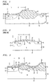
- FIG. 1 is a cross-sectional view of a prior art LDMOS showing an edge of the gate electrode over a gate oxide containing a step;
- FIG. 2 is a cross-sectional view of a prior art LDMOS showing an edge of the gate electrode over two gate oxide thicknesses t 1 and t 2 where t 2 ⁇ 2t 1 (typically).
- FIG. 3 is a cross-sectional view of an LDMOS showing the edge of the gate electrode over a tapered oxide, for one embodiment of the invention.
- the invention includes a selective oxidation that self-aligns a thick, tapered oxide region to a gate electrode edge.
- a nitride layer is placed over the entire wafer and an opening is patterned and subsequently etched into the nitride. One side of the opening is placed over the gate electrode and the other is placed some distance W away.
- the wafer is then oxidized to grow a thicker, tapered (or graded) oxide under the gate electrode.
- the nitride layer is then removed conventionally, such as with a phosphoric acid etch.
- the thicker, tapered oxide is the result of oxidation of both the polysilicon gate and the substrate silicon.
- an asymmetric-graded (or tapered) gate oxide is desired such that the oxide thickness is greater on the drain side of the gate than in the channel region next to the source.
- FIG. 1 is a cross-sectional view of a prior art LDMOS device 1 .
- Device 1 deviates from using a gate oxide 8 of uniform thickness by placing one edge of the gate 10 , of gate width 4 , over a region of thicker oxide (thicker than gate oxide), the field oxide 6 .
- the source 5 , the drain 7 , N + regions 9 and 11 , P region 13 and an N-well drift region 19 in a substrate 23 are also shown.
- gate width 4 is typically greater than 1 to 1.5 microns and the channel region is large because of the misalignment tolerance between the gate electrode 10 and the transition region between the thin gate oxide 2 and the thick field oxide 6 .
- the gate-drain overlap capacitance is large because of the deleterious existence of a region of gate oxide 20 above the N (drift region) 21 near drain 7 and the region of gate electrode 10 above the thick field oxide 6 , thus limiting the high frequency performance of the device. This compromises the speed of the device so that it operates at less than 1 GHz.
- FIG. 2 is a cross-sectional view of yet another prior art LDMOS device 2 .
- a gate oxide 27 is provided that has a step in thickness, t 1 and t 2 .
- the gate-drain overlap capacitance is large in device 2 because t 2 of oxide 27 is approximately equal to 2t 1 of oxide 29 , again limiting the high frequency performance of the device to less than 1 GHz.
- FIG. 3 shows an exemplary device 3 having a tapered oxide 31 as part of the gate oxide 8 , distinct from the field oxide 6 , for one embodiment of the invention.
- the taper oxide 31 is grown after the gate electrode 10 is deposited, the gate electrode 10 is preferably made of doped polysilicon.
- the tapered oxide 31 is formed by depositing a mask 33 , such as silicon nitride, and patterning an opening in the mask adjacent to the gate electrode 10 .
- the mask 33 is patterned such that one side of the opening is placed over the gate electrode 10 and the other side of the opening is placed some distance away from the gate electrode 10 .
- the polysilicon gate electrode 10 is aligned to the existing field (LOCOS or isolation) oxide 6 .
- the tapered (or graded) oxide 31 is then grown by thermal oxidation or oxygen implant, for example. In a preferred embodiment, the mask 33 is then removed.
- the tapered oxide 31 is distinct from the field oxide 6 and is less than 500 nm thick at its thickest point. 200 to 250 nm is preferred. The field oxide 6 of the prior art would typically be greater than 500 nm at its thickest point.
- the structure of FIG. 3 can typically have a gate width 35 less than 1 micron.
- the structure can easily be realized with a gate width 35 equal to 0.3 micron and even less.
- the device 3 has an f T (unity gain frequency) above 10 GHz.
- the LDMOS structure of FIG. 3 reduces the disadvantages of the prior art without negatively affecting the threshold voltage or transconductance of the LDMOS.
- the gate width 35 could be adjusted to control the electric field at high drain-source voltage near the N-N + transition 37 , which may be the region where breakdown occurs.
- a device of the present invention will also comprise an N lightly dope drain (LDD) 39 .
- LDD lightly dope drain
- FIG. 3 shows oxide 31 (silicon dioxide) on the side of the polysilicon gate, which does not occur when the field oxide is grown before gate electrode deposition, as in the prior art.
- An alternative embodiment is to deposit a gate electrode, deposit a hardmask, such as silicon nitride, and pattern the hardmask to provide an opening in the mask adjacent to the gate electrode such that one side of the opening is placed over the gate electrode and the other side of the opening is placed some distance away from the gate electrode.
- Tapered oxide is then grown simultaneously with field oxide growth.
- the tapered oxide may itself be used to perform the function, device isolation, of the field oxide.
Landscapes
- Insulated Gate Type Field-Effect Transistor (AREA)
Abstract
Description
Claims (9)
Priority Applications (2)
| Application Number | Priority Date | Filing Date | Title |
|---|---|---|---|
| US09/641,086 US6506641B1 (en) | 2000-08-17 | 2000-08-17 | Use of selective oxidation to improve LDMOS power transistors |
| US10/300,254 US6762457B2 (en) | 2000-08-17 | 2002-11-20 | LDMOS device having a tapered oxide |
Applications Claiming Priority (1)
| Application Number | Priority Date | Filing Date | Title |
|---|---|---|---|
| US09/641,086 US6506641B1 (en) | 2000-08-17 | 2000-08-17 | Use of selective oxidation to improve LDMOS power transistors |
Related Child Applications (1)
| Application Number | Title | Priority Date | Filing Date |
|---|---|---|---|
| US10/300,254 Division US6762457B2 (en) | 2000-08-17 | 2002-11-20 | LDMOS device having a tapered oxide |
Publications (1)
| Publication Number | Publication Date |
|---|---|
| US6506641B1 true US6506641B1 (en) | 2003-01-14 |
Family
ID=24570875
Family Applications (2)
| Application Number | Title | Priority Date | Filing Date |
|---|---|---|---|
| US09/641,086 Expired - Lifetime US6506641B1 (en) | 2000-08-17 | 2000-08-17 | Use of selective oxidation to improve LDMOS power transistors |
| US10/300,254 Expired - Lifetime US6762457B2 (en) | 2000-08-17 | 2002-11-20 | LDMOS device having a tapered oxide |
Family Applications After (1)
| Application Number | Title | Priority Date | Filing Date |
|---|---|---|---|
| US10/300,254 Expired - Lifetime US6762457B2 (en) | 2000-08-17 | 2002-11-20 | LDMOS device having a tapered oxide |
Country Status (1)
| Country | Link |
|---|---|
| US (2) | US6506641B1 (en) |
Cited By (2)
| Publication number | Priority date | Publication date | Assignee | Title |
|---|---|---|---|---|
| CN102420142A (en) * | 2011-06-07 | 2012-04-18 | 上海华力微电子有限公司 | Method for optimizing source leak punchthrough performance of high-pressure LDMOS (lateral double-diffused metal Oxide semiconductor transistor) device |
| CN110137248A (en) * | 2019-05-29 | 2019-08-16 | 电子科技大学 | A kind of LDMOS device of resistant to total dose effect |
Families Citing this family (5)
| Publication number | Priority date | Publication date | Assignee | Title |
|---|---|---|---|---|
| DE102009051745B4 (en) | 2009-11-03 | 2017-09-21 | Austriamicrosystems Ag | High-voltage transistor with multiple dielectric and manufacturing process |
| US9337310B2 (en) | 2014-05-05 | 2016-05-10 | Globalfoundries Inc. | Low leakage, high frequency devices |
| US10050115B2 (en) | 2014-12-30 | 2018-08-14 | Globalfoundries Inc. | Tapered gate oxide in LDMOS devices |
| JP7815134B2 (en) * | 2020-10-29 | 2026-02-17 | ローム株式会社 | Semiconductor Devices |
| CN112786685B (en) * | 2021-02-08 | 2022-10-21 | 成都芯源系统有限公司 | Transverse double-diffusion transistor with multi-stage field plate and manufacturing method thereof |
Citations (1)
| Publication number | Priority date | Publication date | Assignee | Title |
|---|---|---|---|---|
| US5783474A (en) * | 1995-02-17 | 1998-07-21 | International Rectifier Corporation | Reduced mask process for manufacture of MOS gated devices using dopant-enhanced-oxidation of semiconductor |
Family Cites Families (4)
| Publication number | Priority date | Publication date | Assignee | Title |
|---|---|---|---|---|
| JPH02283072A (en) * | 1989-04-25 | 1990-11-20 | Fuji Electric Co Ltd | Semiconductor device using offset gate type mosfet |
| US5378912A (en) * | 1993-11-10 | 1995-01-03 | Philips Electronics North America Corporation | Lateral semiconductor-on-insulator (SOI) semiconductor device having a lateral drift region |
| US5777363A (en) * | 1993-11-29 | 1998-07-07 | Texas Instruments Incorporated | Semiconductor device with composite drift region |
| KR100253075B1 (en) * | 1997-05-15 | 2000-04-15 | 윤종용 | High breakdown voltage semiconductor device and manufacturing method thereof |
-
2000
- 2000-08-17 US US09/641,086 patent/US6506641B1/en not_active Expired - Lifetime
-
2002
- 2002-11-20 US US10/300,254 patent/US6762457B2/en not_active Expired - Lifetime
Patent Citations (1)
| Publication number | Priority date | Publication date | Assignee | Title |
|---|---|---|---|---|
| US5783474A (en) * | 1995-02-17 | 1998-07-21 | International Rectifier Corporation | Reduced mask process for manufacture of MOS gated devices using dopant-enhanced-oxidation of semiconductor |
Cited By (2)
| Publication number | Priority date | Publication date | Assignee | Title |
|---|---|---|---|---|
| CN102420142A (en) * | 2011-06-07 | 2012-04-18 | 上海华力微电子有限公司 | Method for optimizing source leak punchthrough performance of high-pressure LDMOS (lateral double-diffused metal Oxide semiconductor transistor) device |
| CN110137248A (en) * | 2019-05-29 | 2019-08-16 | 电子科技大学 | A kind of LDMOS device of resistant to total dose effect |
Also Published As
| Publication number | Publication date |
|---|---|
| US20030100165A1 (en) | 2003-05-29 |
| US6762457B2 (en) | 2004-07-13 |
Similar Documents
| Publication | Publication Date | Title |
|---|---|---|
| US5087581A (en) | Method of forming vertical FET device with low gate to source overlap capacitance | |
| US6503805B2 (en) | Channel implant through gate polysilicon | |
| EP0059848B1 (en) | Fet and method for manufacturing such | |
| US4373965A (en) | Suppression of parasitic sidewall transistors in locos structures | |
| JPH0448640A (en) | Manufacture of mos transistor | |
| US6495406B1 (en) | Method of forming lightly doped drain MOS transistor including forming spacers on gate electrode pattern before exposing gate insulator | |
| US6506641B1 (en) | Use of selective oxidation to improve LDMOS power transistors | |
| US20090065859A1 (en) | Trench transistor and method for manufacturing the same | |
| US5641695A (en) | Method of forming a silicon carbide JFET | |
| US5512499A (en) | Method of making symmetrical and asymmetrical MESFETS | |
| US5824575A (en) | Semiconductor device and method of manufacturing the same | |
| US5640029A (en) | Field-effect transistor and method of producing same | |
| KR100916120B1 (en) | Most transistor manufacturing method | |
| JPH07297275A (en) | Method for manufacturing semiconductor device | |
| KR940004415B1 (en) | Making method and structure of mosfet | |
| KR100464535B1 (en) | A method for forming a transistor of a semiconductor device | |
| JP3062421B2 (en) | Semiconductor device and manufacturing method thereof | |
| KR100256228B1 (en) | Separator Formation Method of Semiconductor Device | |
| KR20010064328A (en) | Method for fabricating MOS transistor with ITLDD structure | |
| KR940006082B1 (en) | Semiconductor device isolation method | |
| KR100380979B1 (en) | Manufacturing method for semiconductor device | |
| KR100192596B1 (en) | Buried type transistor and manufacturing method thereof | |
| US7675128B2 (en) | Method for forming a gate insulating layer of a semiconductor device | |
| KR960012262B1 (en) | Mos transistor manufacturing method | |
| JP3035969B2 (en) | Method for manufacturing compound semiconductor device |
Legal Events
| Date | Code | Title | Description |
|---|---|---|---|
| AS | Assignment |
Owner name: LUCENT TECHNOLOGIES INC., NEW JERSEY Free format text: ASSIGNMENT OF ASSIGNORS INTEREST;ASSIGNORS:PEARCE, CHARLES WALTER;SHIBIB, MUHAMMED AYMAN;REEL/FRAME:011428/0941;SIGNING DATES FROM 20001030 TO 20001205 |
|
| FEPP | Fee payment procedure |
Free format text: PAYOR NUMBER ASSIGNED (ORIGINAL EVENT CODE: ASPN); ENTITY STATUS OF PATENT OWNER: LARGE ENTITY |
|
| STCF | Information on status: patent grant |
Free format text: PATENTED CASE |
|
| FPAY | Fee payment |
Year of fee payment: 4 |
|
| FPAY | Fee payment |
Year of fee payment: 8 |
|
| AS | Assignment |
Owner name: DEUTSCHE BANK AG NEW YORK BRANCH, AS COLLATERAL AGENT, NEW YORK Free format text: PATENT SECURITY AGREEMENT;ASSIGNORS:LSI CORPORATION;AGERE SYSTEMS LLC;REEL/FRAME:032856/0031 Effective date: 20140506 Owner name: DEUTSCHE BANK AG NEW YORK BRANCH, AS COLLATERAL AG Free format text: PATENT SECURITY AGREEMENT;ASSIGNORS:LSI CORPORATION;AGERE SYSTEMS LLC;REEL/FRAME:032856/0031 Effective date: 20140506 |
|
| FPAY | Fee payment |
Year of fee payment: 12 |
|
| AS | Assignment |
Owner name: AVAGO TECHNOLOGIES GENERAL IP (SINGAPORE) PTE. LTD., SINGAPORE Free format text: ASSIGNMENT OF ASSIGNORS INTEREST;ASSIGNOR:AGERE SYSTEMS LLC;REEL/FRAME:035365/0634 Effective date: 20140804 Owner name: AVAGO TECHNOLOGIES GENERAL IP (SINGAPORE) PTE. LTD Free format text: ASSIGNMENT OF ASSIGNORS INTEREST;ASSIGNOR:AGERE SYSTEMS LLC;REEL/FRAME:035365/0634 Effective date: 20140804 |
|
| AS | Assignment |
Owner name: AGERE SYSTEMS LLC, PENNSYLVANIA Free format text: TERMINATION AND RELEASE OF SECURITY INTEREST IN PATENT RIGHTS (RELEASES RF 032856-0031);ASSIGNOR:DEUTSCHE BANK AG NEW YORK BRANCH, AS COLLATERAL AGENT;REEL/FRAME:037684/0039 Effective date: 20160201 Owner name: LSI CORPORATION, CALIFORNIA Free format text: TERMINATION AND RELEASE OF SECURITY INTEREST IN PATENT RIGHTS (RELEASES RF 032856-0031);ASSIGNOR:DEUTSCHE BANK AG NEW YORK BRANCH, AS COLLATERAL AGENT;REEL/FRAME:037684/0039 Effective date: 20160201 |
|
| AS | Assignment |
Owner name: BANK OF AMERICA, N.A., AS COLLATERAL AGENT, NORTH CAROLINA Free format text: PATENT SECURITY AGREEMENT;ASSIGNOR:AVAGO TECHNOLOGIES GENERAL IP (SINGAPORE) PTE. LTD.;REEL/FRAME:037808/0001 Effective date: 20160201 Owner name: BANK OF AMERICA, N.A., AS COLLATERAL AGENT, NORTH Free format text: PATENT SECURITY AGREEMENT;ASSIGNOR:AVAGO TECHNOLOGIES GENERAL IP (SINGAPORE) PTE. LTD.;REEL/FRAME:037808/0001 Effective date: 20160201 |
|
| AS | Assignment |
Owner name: AVAGO TECHNOLOGIES GENERAL IP (SINGAPORE) PTE. LTD., SINGAPORE Free format text: TERMINATION AND RELEASE OF SECURITY INTEREST IN PATENTS;ASSIGNOR:BANK OF AMERICA, N.A., AS COLLATERAL AGENT;REEL/FRAME:041710/0001 Effective date: 20170119 Owner name: AVAGO TECHNOLOGIES GENERAL IP (SINGAPORE) PTE. LTD Free format text: TERMINATION AND RELEASE OF SECURITY INTEREST IN PATENTS;ASSIGNOR:BANK OF AMERICA, N.A., AS COLLATERAL AGENT;REEL/FRAME:041710/0001 Effective date: 20170119 |
|
| AS | Assignment |
Owner name: BELL SEMICONDUCTOR, LLC, ILLINOIS Free format text: ASSIGNMENT OF ASSIGNORS INTEREST;ASSIGNORS:AVAGO TECHNOLOGIES GENERAL IP (SINGAPORE) PTE. LTD.;BROADCOM CORPORATION;REEL/FRAME:044886/0001 Effective date: 20171208 Owner name: BELL SEMICONDUCTOR, LLC, ILLINOIS Free format text: ASSIGNMENT OF ASSIGNORS INTEREST;ASSIGNORS:AVAGO TECHNOLOGIES GENERAL IP (SINGAPORE) PTE. LTD.;BROADCOM CORPORATION;REEL/FRAME:044886/0608 Effective date: 20171208 |
|
| AS | Assignment |
Owner name: CORTLAND CAPITAL MARKET SERVICES LLC, AS COLLATERAL AGENT, ILLINOIS Free format text: SECURITY INTEREST;ASSIGNORS:HILCO PATENT ACQUISITION 56, LLC;BELL SEMICONDUCTOR, LLC;BELL NORTHERN RESEARCH, LLC;REEL/FRAME:045216/0020 Effective date: 20180124 Owner name: CORTLAND CAPITAL MARKET SERVICES LLC, AS COLLATERA Free format text: SECURITY INTEREST;ASSIGNORS:HILCO PATENT ACQUISITION 56, LLC;BELL SEMICONDUCTOR, LLC;BELL NORTHERN RESEARCH, LLC;REEL/FRAME:045216/0020 Effective date: 20180124 |
|
| AS | Assignment |
Owner name: BELL NORTHERN RESEARCH, LLC, ILLINOIS Free format text: SECURITY INTEREST;ASSIGNOR:CORTLAND CAPITAL MARKET SERVICES LLC;REEL/FRAME:060885/0001 Effective date: 20220401 Owner name: BELL SEMICONDUCTOR, LLC, ILLINOIS Free format text: SECURITY INTEREST;ASSIGNOR:CORTLAND CAPITAL MARKET SERVICES LLC;REEL/FRAME:060885/0001 Effective date: 20220401 Owner name: HILCO PATENT ACQUISITION 56, LLC, ILLINOIS Free format text: SECURITY INTEREST;ASSIGNOR:CORTLAND CAPITAL MARKET SERVICES LLC;REEL/FRAME:060885/0001 Effective date: 20220401 Owner name: BELL NORTHERN RESEARCH, LLC, ILLINOIS Free format text: RELEASE BY SECURED PARTY;ASSIGNOR:CORTLAND CAPITAL MARKET SERVICES LLC;REEL/FRAME:059720/0719 Effective date: 20220401 Owner name: BELL SEMICONDUCTOR, LLC, ILLINOIS Free format text: RELEASE BY SECURED PARTY;ASSIGNOR:CORTLAND CAPITAL MARKET SERVICES LLC;REEL/FRAME:059720/0719 Effective date: 20220401 Owner name: HILCO PATENT ACQUISITION 56, LLC, ILLINOIS Free format text: RELEASE BY SECURED PARTY;ASSIGNOR:CORTLAND CAPITAL MARKET SERVICES LLC;REEL/FRAME:059720/0719 Effective date: 20220401 |