US6498575B2 - D/A converter - Google Patents
D/A converter Download PDFInfo
- Publication number
- US6498575B2 US6498575B2 US09/921,474 US92147401A US6498575B2 US 6498575 B2 US6498575 B2 US 6498575B2 US 92147401 A US92147401 A US 92147401A US 6498575 B2 US6498575 B2 US 6498575B2
- Authority
- US
- United States
- Prior art keywords
- current
- converter
- constant
- voltage
- switch
- Prior art date
- Legal status (The legal status is an assumption and is not a legal conclusion. Google has not performed a legal analysis and makes no representation as to the accuracy of the status listed.)
- Expired - Lifetime
Links
Images


Classifications
-
- H—ELECTRICITY
- H03—ELECTRONIC CIRCUITRY
- H03M—CODING; DECODING; CODE CONVERSION IN GENERAL
- H03M1/00—Analogue/digital conversion; Digital/analogue conversion
- H03M1/66—Digital/analogue converters
-
- H—ELECTRICITY
- H03—ELECTRONIC CIRCUITRY
- H03M—CODING; DECODING; CODE CONVERSION IN GENERAL
- H03M1/00—Analogue/digital conversion; Digital/analogue conversion
- H03M1/66—Digital/analogue converters
- H03M1/74—Simultaneous conversion
- H03M1/742—Simultaneous conversion using current sources as quantisation value generators
- H03M1/747—Simultaneous conversion using current sources as quantisation value generators with equal currents which are switched by unary decoded digital signals
Definitions
- the present invention is related to a D/A converter for outputting an analog signal in correspondence with a digital input signal.
- D/A converters capable of converting digital signals into analog signals are necessarily required in such digital processing systems, the important aspect of which is considerably increased.
- FIG. 10 shows a structural diagram of an n-bit D/A converter.
- Reference numeral 10 indicates an n-bit digital input signal
- reference numeral 11 represents a decode circuit for outputting “k” pieces of control signals used to select a predetermined current cell circuit in response to the digital input signal 10 .
- Symbol “k” is equal to “2 n ⁇ 1.”
- reference numeral 12 indicates “k” pieces of current cell selection signals which are outputted from the decode circuit 11
- reference numeral 13 represents “k” pieces of current cell circuits which are 25 selected by the current cell selection signal 12 and also own values equal to each other.
- Reference numeral 14 denotes an output current which is produced by adding such output currents of current cell circuits selected by the current cell selection signal 12 among all of the current cell circuits 13
- reference numeral 15 indicates another output current which is produced by adding such output currents of current cell circuits other than the current cell circuits selected by the current cell selection signal 12 among all of the current cell circuits 13 .
- reference numeral 16 shows a current-to-voltage converting circuit for converting the output current 14 into a voltage corresponding thereto
- reference numeral 17 denotes a current-to-voltage converting circuit for converting the output current 15 into a voltage corresponding thereto
- reference numeral 18 represents an analog output terminal from which the voltage converted by the current-to-voltage converting circuit 16 is outputted
- reference numeral 19 shows an analog output terminal from which the voltage converted by the current-to-voltage converting circuit 17 is outputted.
- FIG. 11 is a structural diagram for showing a structure of the current cell circuit 13 .
- Reference numeral 20 shows a current cell selection signal
- reference numeral 21 represents a constant current source for supplying a unit current “i”
- reference numeral 22 indicates a current output terminal to which the current “i” is supplied in the case that the current output terminal is selected by the current cell selection signal 20
- reference numeral 23 indicates a current output terminal to which the current “i” is supplied in such a case that the current output terminal is not selected by the current cell selection signal 20 .
- reference numeral 24 shows a Pch transistor having a switch function and connected to a current path provided on the side of the current output terminal 22
- reference numeral 25 represents another Pch transistor having a switch function and connected to a current path provided on the side of the current output terminal 23
- reference numeral 26 shows an inverter for inverting the current cell selection signal 20 which is supplied to the gate of the Pch transistor 24 .
- the current cell selection signal 20 is supplied to the gate of the Pch transistor 25 , and also is supplied via the inverter 26 to the gate of the Pch transistor 24 so as to activate the switch function of any one of the current paths of the current cell circuits, so that the output currents derived from the current output terminals 22 and 23 are controlled.
- FIG. 12 shows a relationship explanatory diagram for explaining the current cell selection signal 20 (SEL), and values of currents supplied to both the current output terminal 22 and the current output terminal 23 .
- FIG. 13 is a structural diagram of the current-to-voltage converting circuits 16 and 17 .
- Reference numeral 40 indicates a current input terminal
- reference numeral 41 shows an input current having a current value “I”
- reference numeral 42 indicates a resistive element having a resistance value “R”
- reference numeral 43 indicates a voltage output terminal.
- the present invention has been made to solve the above-explained structural problems, and therefore, has an object to provide such a D/A converter capable of reducing an occupied area of a circuit and at the same time capable of improving resolution by largely reducing a total number of circuit components thereof, as compared with the structure of the conventional D/A converter.
- a D/A converter is featured by such a D/A converter comprising: a constant current source (constant current source 503 ); a switch group constituted by switch circuits (switch circuit 504 ), which is series-connected to the constant current source, and is operated in response to a control signal (current path selection signal 502 ) to form a plurality of current paths for equally dividing a constant current of the constant current source; decode means (decode circuit 501 ) for outputting the control signal used to control operations of the switch circuits in response to a digital input signal (digital input signal 500 ); and current-to-voltage converting means (current/voltage converting circuit 508 ) for adding currents to each other which are outputted via the current paths of the switch circuits so as to convert the added currents into a voltage.
- a D/A converter is featured by that in the D/A converter, the constant current is obtained by employing a resistive element (resistive element 511 ) having one end to which a constant voltage is added instead of the constant current source.
- a resistive element resistive element 511
- a D/A converter is featured by that in the D/A converter, the constant current source is a single constant current source; the switch circuit includes: a plurality of lower-stage switching elements (Pch transistors 73 , 74 ) for forming the plurality of current paths; and an upper-stage switching element (Pch transistor 77 ) which is series-connected to an upper stage of each of the lower-stage switching elements, and forms a current path for determining a shunt value of the constant currents supplied to the plurality of current paths; and the decode means outputs such a control signal (upper-stage current path selection signal 78 , low-stage current path selection signals 71 , 72 ) capable of independently controlling the respective switching elements.
- the control signal upper-stage current path selection signal 78 , low-stage current path selection signals 71 , 72
- a D/A converter is featured by that in the D/A converter, a plurality of D/A converters (D/A converter 603 ) are connected in parallel to each other; and the D/A converter is comprised of decode means (decode circuit 601 ) for outputting such a signal (D/A converter control signal 602 ) used to control the respective decode means which constitute the D/A converters in response to a digital input signal (digital input signal 600 ), respectively.
- decode circuit 601 for outputting such a signal (D/A converter control signal 602 ) used to control the respective decode means which constitute the D/A converters in response to a digital input signal (digital input signal 600 ), respectively.
- a D/A converter is featured by that in the D/A converter, the switch circuit includes: a Pch transistor (Pch transistors 73 , 74 , 77 ) for constituting each of the switching elements; and a switch (SW 1 , SW 2 , SW 3 ) for selecting a constant voltage (bias voltage 77 , 80 ) by which the Pch transistor is operated in a saturation region and for applying the selected constant voltage to a gate of the Pch transistor when the switching element is selectively turned ON in response to the control signal.
- a Pch transistor Pch transistors 73 , 74 , 77
- SW 1 , SW 2 , SW 3 for selecting a constant voltage (bias voltage 77 , 80 ) by which the Pch transistor is operated in a saturation region and for applying the selected constant voltage to a gate of the Pch transistor when the switching element is selectively turned ON in response to the control signal.
- a D/A converter is featured by that in the D/A converter, the current-to-voltage converting means (current/voltage converting circuit 507 , 508 ) maintains a potential at the output terminal of the switch circuit at a constant value by keeping a potential at the input terminal (current input terminal 90 ) of the current-to-voltage converting means constant (reference voltage VREF).
- the current-to-voltage converting means current/voltage converting circuit 507 , 508
- the current-to-voltage converting means maintains a potential at the output terminal of the switch circuit at a constant value by keeping a potential at the input terminal (current input terminal 90 ) of the current-to-voltage converting means constant (reference voltage VREF).
- a D/A converter is featured by that in the D/A converter, the decode means selects the switch circuit in response to the digital input signal, and also outputs such a control signal used to supply a unit current to the switch circuit, the unit current being produced by shunting the constant current in correspondence with a total number of the selected switch circuits.
- the constant current is supplied to the switch circuits, and the constant current is equally distributed to a plurality of current paths of the switch circuits in response to the digital input signal, so that the output current value can be varied.
- the current value is increased/decreased in the unit of the constant current, whereas the current value can be increased/decreased based upon such a unit current produced by equally dividing the constant current, and also the resolution can be improved without increasing a total number of the constant current sources. While the resolution may be determined based upon a total number of these current paths, in the case that the constant current is divided into two current paths, the resulting resolution can be increased by 1 bit (namely, two times).
- the necessary occupied area of the D/A converter according to the present invention may be reduced by 1 ⁇ 2, or less.
- the resultant resolution may be increased more than two times higher than that of the prior art.
- the constant current of a single constant current source is shunted in correspondence with a total number of the switch circuits which are selected by operating the upper-stage switching elements. Furthermore, the shunted current is subdivided based upon a total number of such current paths which are formed by operating the lower-stage switching elements so as to obtain the unit current. As a consequence, the resolution can be improved without increasing a total number of these constant current sources.
- the current is variable in response to the quantity of these switch circuits, which is supplied to the current paths which form the unit current. As a result, the resolution in the vicinity of the center can be increased, as compared with that of the conventional structure. Also, since the unit current can be varied, the resolution can be readily changed, whereas the resolution of the conventional D/A converter is changed by controlling the capacity of the constant current source.
- the current can be equally divided into the respective current paths irrespective of the characteristics of the respective switching elements (transistors).
- the potential at the input terminal of the current-to-voltage converting means is kept constant, the potential at the output terminal of the switch circuit can also be kept constant, which is connected to the input terminal.
- the current which flows through the current paths of the switch circuits can be equally divided in high precision.
- such a decode means can be obtained which may allocate the digital input signal to the analog output in such a manner that the quantizing noise in the vicinity of the center can become minimum in response to such an output signal as a sine wave having a large changing ratio in the vicinity of a center of this sine wave.
- FIG. 1 is a structural diagram as to a D/A converter according to a first embodiment mode of the present invention.
- FIG. 2 is a structural diagram as to a switch circuit of the D/A converter according to the first embodiment mode of the present invention.
- FIG. 3 is an explanatory diagram for explaining operations of the switch circuit of the D/A converter according to the first embodiment mode of the present invention.
- FIG. 4 is a structural diagram as to a D/A converter according to a second embodiment mode of the present invention.
- FIG. 5 is a structural diagram as to a switch circuit of the D/A converter according to a third embodiment mode of the present invention.
- FIG. 6 is a structural diagram as to a D/A converter according to a fourth embodiment mode of the present invention.
- FIG. 7 is a structural diagram as to a switch circuit of a D/A converter according to a fifth embodiment mode of the present invention.
- FIG. 8 is a structural diagram as to a switch circuit of the D/A converter according to the fifth embodiment mode of the present invention.
- FIG. 9 is a structural diagram for showing a current-to-voltage converting circuit of a D/A converter according to a sixth embodiment mode of the present invention.
- FIG. 10 is a structural diagram for representing the conventional D/A converter.
- FIG. 11 is a structural diagram for showing the current cell circuit employed in the conventional D/A converter.
- FIG. 12 is an explanatory diagram for explaining operations of the current cell circuit employed in the conventional D/A converter.
- FIG. 13 is a structural diagram for indicating the current-to-voltage converting circuit employed in the conventional D/A converter.
- FIG. 1 is a structural diagram of an n-bit D/A converter according to a first embodiment mode of the present invention.
- reference numeral 500 shows an n-bit digital input signal
- reference numeral 501 represents a decode circuit for outputting “2 ⁇ k” pieces of control signals which are used to control a total number of current paths in response to the digital input signal 500 (symbol “k” is equal to “2 n ⁇ 1”)
- reference numeral 502 represents “k” pieces of current path selection signals outputted from the decode circuit 501
- reference numeral 503 indicates a constant current source for supplying (k ⁇ i) currents
- reference numeral 504 shows “k” pieces of switch circuits which are selected by the current path selection signal 502 .
- reference numeral 505 is an output current produced by adding output currents derived from one current path within the two current paths in all of the current switch circuits 504
- reference numeral 506 represents an output current produced by adding all of output currents derived from such current paths located opposite to the side of the output current 505 within the two current paths in all of the switch circuits 504 .
- reference numeral 507 shows a current-to-voltage converting circuit for converting the output current 505 into a voltage corresponding thereto
- reference numeral 508 denotes a current-to-voltage converting circuit for converting the output current 506 into a voltage corresponding thereto
- reference numeral 509 represents an analog output terminal from which the voltage converted by the current-to-voltage converting circuit 507 is outputted
- reference numeral 510 shows an analog output terminal from which the voltage converted by the current-to-voltage converting circuit 508 is outputted.
- FIG. 2 is a structural diagram of the switch circuit 504 .
- reference numeral 70 shows a current input terminal
- reference numerals 71 and 72 indicate current path selection signals
- reference numeral 73 represents a Pch transistor having a switch function, which is connected to the side of the current path selection signal 71 .
- reference numeral 74 denotes a Pch transistor having the same characteristic as that of the Pch transistor 73 having the switch function, which is connected to the side of the current path selection signal 72
- reference numeral 75 represents a current output terminal to which a current is supplied when this current output terminal is selected by the current path selection signal 71
- reference numeral 76 indicates a current output terminal to which a current is supplied when this current output terminal is selected by the current path selection signal 72 .
- FIG. 3 represents a relationship diagram for explaining a relationship among the current path selection signal 71 (SEL 1 ), the current path selection signal 72 (SEL 2 ), a value of a current flowing through the current input terminal 70 , a value of a current outputted to the current output terminal 75 , and a value of a current outputted to the current output terminal 76 .
- the Pch transistor 73 (TP 1 ) is turned ON and the Pch transistor 74 (TP 2 ) is turned ON, so that a total number of the current paths becomes 2 . Since the Pch transistor 73 (TP 1 ) and the Pch transistor 74 (TP 2 ) own the same characteristics, the impedances thereof, as viewed from the current input terminal 70 , are made identical to each other. Assuming now that the current value supplied to the current input terminal 70 is “is”, a current value “is/2” which is obtained by equally dividing this current value “is” is supplied to both the current output terminal 75 and the current output terminal 76 .
- the currents may be added to the output current 505 in the unit of the current “i” which passed through each of the current paths. Since a total number of the switch circuits 504 is equal to “k” pieces, the gradation of the output currents from the switch circuits 504 becomes “2 n ”, namely such a D/A converter having n-bit resolution can be realized.
- FIG. 4 is a structural diagram of an n-bit D/A converter according to a second embodiment mode of the present invention. That is, in the D/A converter of the first embodiment mode, a resistive element 511 is newly provided instead of the constant current source, and a constant voltage is applied to a constant voltage input terminal 512 which constitutes one end of this resistive element 511 , so that the n-bit D/A converter of the second embodiment mode operable in a similar manner to that of the first embodiment mode may be realized. Since the D/A converter no longer requires the constant current source by employing this circuit arrangement, the circuit area thereof can be further reduced.
- FIG. 5 indicates a D/A converter according to a third embodiment mode of the present invention.
- This D/A converter of the third embodiment mode is arranged by that a Pch transistor 77 is series-connected to the switch circuit 504 of the D/A converter according to the first embodiment mode, and an upper-stage current path selection signal 78 is inputted to the gate of the Pch transistor 77 .
- the D/A converter having this switch circuit is equivalent to the D/A converter in FIG. 1 whose decode circuit is replaced by such a decode circuit for outputting the upper-stage current path selection signal to the respective switch circuits.
- the operation of the D/A converter with employment of this arrangement is featured by that resolution in the vicinity of the center can be further improved, as compared with that of the D/A converter of the first embodiment mode because of the following reason. That is, such a current which is equally divided by the number equal to a total number of such current paths which are turned ON by receiving the upper-stage current path selection signal may be furthermore and equally subdivided by a lower-stage switch. Other operations of this D/A converter are identical to those of the first embodiment mode.
- FIG. 6 is a structural diagram of an n-bit D/A converter according to a fourth embodiment mode of the present invention.
- This D/A converter of the fourth embodiment mode is featured by such a D/A converter constituted by employing a plurality of the above-explained D/A converters as recited in the embodiment modes 1, 2, 3 of the present invention.
- reference numeral 600 shows an n-bit digital input signal
- reference numeral 601 indicates a decode circuit for outputting a signal used to control a plurality of D/A converters 603 of the present invention in response to the digital input signal 600 .
- reference numeral 602 represents a D/A converter control signal outputted from the decode circuit 601
- reference numeral 604 shows one output current summation calculated in all of the D/A converters 603
- reference numeral 605 indicates the other output current summation calculated in all of the D/A converters.
- reference numeral 606 shows a current-to-voltage converting circuit for converting the output current 604 into a voltage corresponding thereto
- reference numeral 607 denotes a current-to-voltage converting circuit for converting the output current 605 into a voltage corresponding thereto
- reference numeral 608 represents an analog output terminal from which the voltage converted by the current-to-voltage converting circuit 606 is outputted
- reference numeral 609 shows an analog output terminal from which the voltage converted by the current-to-voltage converting circuit 607 is outputted.
- FIG. 7 is a structural diagram of a switch circuit according to claim 5 of the present invention. It should be understood that since descriptions of reference numerals shown in FIG. 7 are the same as those of FIG. 2, these explanations are omitted.
- This switch circuit is controlled in the following manner. That is, when the switches SW 1 and SW 2 are turned ON in response to the current path selection signals 71 and 72 , such a bias voltage 77 is applied to gates of respective Pch transistors 73 and 74 by which these Pch transistors 73 and 74 are operable in a saturation region, whereas when the switches SW 1 and SW 2 are turned OFF, this bias voltage 77 is fixed to a power supply voltage VDD.
- currents which flow through the respective current paths may be determined based upon a potential difference between the current input terminal 70 and the bias voltage 77 irrespective of such a fact that the potential at the current output terminal 75 is not made coincident with the potential at the current output terminal 76 .
- FIG. 8 is a structural diagram of a switch circuit arranged by employing the switch circuit shown in FIG. 5 . It should be noted that in FIG. 8, explanations of reference numerals applied to the same components of FIG. 5 are omitted.
- reference numeral 79 indicates a bias voltage 1 . This bias voltage 1 is applied to the gates of the Pch transistors 73 and 74 which constitute a lower-stage switch circuit when switches SW 1 and SW 2 are turned ON.
- reference numeral 80 represents another bias voltage 2 . This bias voltage 2 is applied to a gate of a Pch transistor 77 which constitutes an upper-stage switch circuit when a switch SW 3 is turned ON.
- the respective bias voltages are such voltages which are adjusted in such a manner that the Pch transistors are operable in the saturation region.
- the current may be equally subdivided to the respective current paths irrespective of the states of the respective switch circuits.
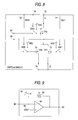
- FIG. 9 is a structural diagram for showing a current-to-voltage converting circuit according to claim 6 of the present invention.
- reference numeral 90 indicates a current input terminal
- reference numeral 91 shows an input current which is entered from the current input terminal 90
- reference numeral 92 indicates a resistive element having a resistance value R
- reference numeral 93 represents a voltage output terminal from which a voltage corresponding to the input current 91 is outputted.
- reference numeral 94 is an operational amplifying circuit
- reference numeral 95 represents a reference voltage (VREF) which is inputted to a non-inverting terminal (+) of the operational amplifier.
- VREF reference voltage
- the current-to-voltage converting operation of this current-to-voltage converting circuit is performed as follows: That is, since a potential at the current input terminal 90 is maintained at the reference voltage VREF by the operational amplifying circuit 94 , such a differential voltage defined by “VREF-R ⁇ i” is outputted from the voltage output terminal 93 , so that an input current “i” is converted into such an output voltage corresponding to this current “i.” Since this current-voltage converting circuit is employed, the potential at the current input terminal 90 is kept at a constant potential. As a consequence, the potential differences at the upper ends of the switch circuits which are connected to the respective current paths are identical to each other, the currents may be equally divided into the respective current paths.
- the occupied area of the D/A converter can be made smaller than that of the conventional D/A converter. This will make it possible, in such a technical field of digital mobile communication terminal apparatuses which are known as digital processing systems, to make the terminal apparatuses more compact and lighter.
- the unit current is variable in response to the digital input signal, the resolution in the vicinity of the center can be largely improved, as compared with that of the conventional D/A converter.
Abstract
Description
Claims (8)
Applications Claiming Priority (2)
| Application Number | Priority Date | Filing Date | Title |
|---|---|---|---|
| JP2000-236996 | 2000-08-04 | ||
| JP2000236996A JP3494366B2 (en) | 2000-08-04 | 2000-08-04 | DA converter |
Publications (2)
| Publication Number | Publication Date |
|---|---|
| US20020014984A1 US20020014984A1 (en) | 2002-02-07 |
| US6498575B2 true US6498575B2 (en) | 2002-12-24 |
Family
ID=18728940
Family Applications (1)
| Application Number | Title | Priority Date | Filing Date |
|---|---|---|---|
| US09/921,474 Expired - Lifetime US6498575B2 (en) | 2000-08-04 | 2001-08-03 | D/A converter |
Country Status (5)
| Country | Link |
|---|---|
| US (1) | US6498575B2 (en) |
| EP (1) | EP1189353B1 (en) |
| JP (1) | JP3494366B2 (en) |
| KR (1) | KR100760527B1 (en) |
| DE (1) | DE60126877T2 (en) |
Cited By (4)
| Publication number | Priority date | Publication date | Assignee | Title |
|---|---|---|---|---|
| US20040222985A1 (en) * | 2002-12-10 | 2004-11-11 | Hajime Kimura | Semiconductor device, digital-analog converter and display device thereof |
| WO2005041417A2 (en) * | 2003-10-27 | 2005-05-06 | Dan Raphaeli | Digital input signals constructor providing analog representation thereof |
| US20060244646A1 (en) * | 2005-04-28 | 2006-11-02 | Kawasaki Microelectronics, Inc. | D/A converter |
| US20180205387A1 (en) * | 2013-04-05 | 2018-07-19 | Maxlinear, Inc. | Multi-zone data converters |
Families Citing this family (5)
| Publication number | Priority date | Publication date | Assignee | Title |
|---|---|---|---|---|
| EP1445868B1 (en) | 2003-02-05 | 2006-05-03 | Alcatel | Method for Digital-to-Analogue conversion and Digital-to-Analogue Convertor |
| JP4942012B2 (en) * | 2005-05-23 | 2012-05-30 | ルネサスエレクトロニクス株式会社 | Display device drive circuit and drive method |
| KR100849787B1 (en) | 2006-11-13 | 2008-07-31 | 삼성전기주식회사 | Digital-analog converter being easy to extend resolution |
| US8493251B2 (en) * | 2011-07-28 | 2013-07-23 | Fujitsu Semiconductor Limited | Self-calibrated DAC with reduced glitch mapping |
| CN110932731B (en) * | 2019-11-12 | 2020-09-25 | 深圳信息职业技术学院 | Digital-to-analog conversion device and frequency converter speed regulation system |
Citations (8)
| Publication number | Priority date | Publication date | Assignee | Title |
|---|---|---|---|---|
| US4587477A (en) * | 1984-05-18 | 1986-05-06 | Hewlett-Packard Company | Binary scaled current array source for digital to analog converters |
| US5059977A (en) * | 1990-08-03 | 1991-10-22 | Magnavox Government And Industrial Electronics Company | Synchronizing switch arrangement for a digital-to-analog converter to reduce in-band switching transients |
| US5294929A (en) | 1991-07-18 | 1994-03-15 | Sony Corporation | Control system for peripheral devices |
| JPH08125538A (en) | 1994-10-24 | 1996-05-17 | Nec Corp | Digital/analog converter |
| JPH08265125A (en) | 1995-03-20 | 1996-10-11 | Oki Electric Ind Co Ltd | Current switch circuit |
| US5870049A (en) * | 1997-04-16 | 1999-02-09 | Mosaid Technologies Incorporated | Current mode digital to analog converter |
| JPH11251912A (en) | 1998-02-27 | 1999-09-17 | Hitachi Ltd | Digital/analog converter and current source circuit |
| US6008747A (en) | 1997-09-05 | 1999-12-28 | Rohm Co., Ltd. | Digital-to-analog converter with current source centrally located between a plurality of current mirrors |
Family Cites Families (13)
| Publication number | Priority date | Publication date | Assignee | Title |
|---|---|---|---|---|
| DE3145889A1 (en) * | 1981-11-19 | 1983-05-26 | Siemens AG, 1000 Berlin und 8000 München | INTEGRATED DIGITAL / ANALOG CONVERTER |
| US5023614A (en) * | 1989-09-13 | 1991-06-11 | Advanced Micro Devices, Inc. | Switchable DAC with current surge protection |
| US5148164A (en) * | 1990-04-23 | 1992-09-15 | Mitsubishi Denki Kabushiki Kaisha | Current generating device for complementarily generating two currents of different magnitudes in response to one-bit data |
| KR930009432B1 (en) * | 1991-12-31 | 1993-10-04 | 현대전자산업 주식회사 | Digital/analog converter current unit |
| US5598161A (en) * | 1992-12-18 | 1997-01-28 | Sony Corporation | Analog-to-digital converter having reduced circuit area |
| US5442352A (en) * | 1994-01-14 | 1995-08-15 | Motorola, Inc. | Linear attenuator for current-mode digital-to-analog converter (DAC) or the like |
| JP2872074B2 (en) * | 1995-04-21 | 1999-03-17 | 日本電気アイシーマイコンシステム株式会社 | Digital-to-analog converter |
| JPH08335881A (en) * | 1995-06-06 | 1996-12-17 | Mitsubishi Electric Corp | Complementary current source circuit |
| US5600321A (en) * | 1995-06-07 | 1997-02-04 | Advanced Micro Devices Inc. | High speed, low power CMOS D/A converter for wave synthesis in network |
| US5654710A (en) * | 1995-06-15 | 1997-08-05 | Vlsi Technology, Inc. | Dynamic power reduction digital-to-analog converter and method therefor |
| US5661483A (en) * | 1996-02-29 | 1997-08-26 | Western Digital Corporation | Area integrator servo demodulator with on-chip CMOS analog-to-digital converter |
| US5798723A (en) * | 1996-07-19 | 1998-08-25 | National Semiconductor Corporation | Accurate and precise current matching for low voltage CMOS digital to analog converters |
| JPH11239059A (en) * | 1998-02-20 | 1999-08-31 | Hitachi Ltd | Digital-to-analog converter |
-
2000
- 2000-08-04 JP JP2000236996A patent/JP3494366B2/en not_active Expired - Fee Related
-
2001
- 2001-08-03 EP EP01118913A patent/EP1189353B1/en not_active Expired - Lifetime
- 2001-08-03 DE DE60126877T patent/DE60126877T2/en not_active Expired - Lifetime
- 2001-08-03 US US09/921,474 patent/US6498575B2/en not_active Expired - Lifetime
- 2001-08-03 KR KR1020010046920A patent/KR100760527B1/en not_active IP Right Cessation
Patent Citations (8)
| Publication number | Priority date | Publication date | Assignee | Title |
|---|---|---|---|---|
| US4587477A (en) * | 1984-05-18 | 1986-05-06 | Hewlett-Packard Company | Binary scaled current array source for digital to analog converters |
| US5059977A (en) * | 1990-08-03 | 1991-10-22 | Magnavox Government And Industrial Electronics Company | Synchronizing switch arrangement for a digital-to-analog converter to reduce in-band switching transients |
| US5294929A (en) | 1991-07-18 | 1994-03-15 | Sony Corporation | Control system for peripheral devices |
| JPH08125538A (en) | 1994-10-24 | 1996-05-17 | Nec Corp | Digital/analog converter |
| JPH08265125A (en) | 1995-03-20 | 1996-10-11 | Oki Electric Ind Co Ltd | Current switch circuit |
| US5870049A (en) * | 1997-04-16 | 1999-02-09 | Mosaid Technologies Incorporated | Current mode digital to analog converter |
| US6008747A (en) | 1997-09-05 | 1999-12-28 | Rohm Co., Ltd. | Digital-to-analog converter with current source centrally located between a plurality of current mirrors |
| JPH11251912A (en) | 1998-02-27 | 1999-09-17 | Hitachi Ltd | Digital/analog converter and current source circuit |
Cited By (10)
| Publication number | Priority date | Publication date | Assignee | Title |
|---|---|---|---|---|
| US20040222985A1 (en) * | 2002-12-10 | 2004-11-11 | Hajime Kimura | Semiconductor device, digital-analog converter and display device thereof |
| US7049991B2 (en) * | 2002-12-10 | 2006-05-23 | Semiconductor Energy Laboratory Co., Ltd. | Semiconductor device, digital-analog converter and display device thereof |
| WO2005041417A2 (en) * | 2003-10-27 | 2005-05-06 | Dan Raphaeli | Digital input signals constructor providing analog representation thereof |
| US20070080841A1 (en) * | 2003-10-27 | 2007-04-12 | Dan Raphaeli | Digital input signals constructor providing analog representation thereof |
| US7443326B2 (en) * | 2003-10-27 | 2008-10-28 | Dan Raphaeli | Digital input signals constructor providing analog representation thereof |
| WO2005041417A3 (en) * | 2003-10-27 | 2009-04-02 | Dan Raphaeli | Digital input signals constructor providing analog representation thereof |
| US20060244646A1 (en) * | 2005-04-28 | 2006-11-02 | Kawasaki Microelectronics, Inc. | D/A converter |
| US7256722B2 (en) * | 2005-04-28 | 2007-08-14 | Kawasaki Microelectronics, Inc. | D/A converter |
| US20180205387A1 (en) * | 2013-04-05 | 2018-07-19 | Maxlinear, Inc. | Multi-zone data converters |
| US10447287B2 (en) * | 2013-04-05 | 2019-10-15 | Maxlinear, Inc. | Multi-zone data converters |
Also Published As
| Publication number | Publication date |
|---|---|
| JP2002050966A (en) | 2002-02-15 |
| KR20020011920A (en) | 2002-02-09 |
| KR100760527B1 (en) | 2007-09-20 |
| JP3494366B2 (en) | 2004-02-09 |
| US20020014984A1 (en) | 2002-02-07 |
| EP1189353B1 (en) | 2007-02-28 |
| EP1189353A2 (en) | 2002-03-20 |
| DE60126877T2 (en) | 2007-06-14 |
| EP1189353A3 (en) | 2004-04-14 |
| DE60126877D1 (en) | 2007-04-12 |
Similar Documents
| Publication | Publication Date | Title |
|---|---|---|
| US5870049A (en) | Current mode digital to analog converter | |
| US5801655A (en) | Multi-channel D/A converter utilizing a coarse D/A converter and a fine D/A converter | |
| US5283579A (en) | Digital to analog converter having high multiplying bandwidth | |
| US6433717B1 (en) | D/A resistor strings with cross coupling switches | |
| US8063808B2 (en) | Multi-input operational amplifier circuit, digital/analog converter using same, and driver for display device using same | |
| US5164725A (en) | Digital to analog converter with current sources paired for canceling error sources | |
| US7825843B2 (en) | D/A converter and semiconductor integrated circuit including the same | |
| JP5166375B2 (en) | Digital / analog converter having a circuit architecture for improving switch losses | |
| US6522280B2 (en) | Adjustable digital-to-analog converter | |
| KR940009253B1 (en) | Semiconductor ic device for supplying a bias current to da converters | |
| KR960016160A (en) | Digital-to-analog converter with reduced resistance | |
| US6498575B2 (en) | D/A converter | |
| US4896157A (en) | Digital to analog converter having single resistive string with shiftable voltage thereacross | |
| US5568146A (en) | Digital/analog converter | |
| EP1235352B1 (en) | Digital-to-analog converter | |
| US6344815B2 (en) | Digital-to-analog converter | |
| US20090079609A1 (en) | Digital-to-analog converter | |
| US6999016B2 (en) | D/A converter and semiconductor device | |
| US10511321B2 (en) | Digital-to-analog converter and method for digital-to-analog conversion | |
| US6140953A (en) | D/A converting apparatus with independent D/A converter controlled reference signals | |
| JP2005252663A (en) | Current cell matrix type digital/analog converter | |
| US6897799B1 (en) | Current parking return to zero digital-to-analog converter | |
| US20040125004A1 (en) | D/A converter for converting plurality of digital signals simultaneously | |
| US7256722B2 (en) | D/A converter | |
| US5455580A (en) | Circuit device utilizing a plurality of transistor pairs |
Legal Events
| Date | Code | Title | Description |
|---|---|---|---|
| AS | Assignment |
Owner name: MATSUSHITA ELECTRIC INDUSTRIAL CO., LTD., JAPAN Free format text: ASSIGNMENT OF ASSIGNORS INTEREST;ASSIGNOR:MATSUSAKA, HIROMI;REEL/FRAME:012149/0183 Effective date: 20010830 |
|
| FEPP | Fee payment procedure |
Free format text: PAYOR NUMBER ASSIGNED (ORIGINAL EVENT CODE: ASPN); ENTITY STATUS OF PATENT OWNER: LARGE ENTITY |
|
| STCF | Information on status: patent grant |
Free format text: PATENTED CASE |
|
| FEPP | Fee payment procedure |
Free format text: PAYER NUMBER DE-ASSIGNED (ORIGINAL EVENT CODE: RMPN); ENTITY STATUS OF PATENT OWNER: LARGE ENTITY Free format text: PAYOR NUMBER ASSIGNED (ORIGINAL EVENT CODE: ASPN); ENTITY STATUS OF PATENT OWNER: LARGE ENTITY |
|
| FPAY | Fee payment |
Year of fee payment: 4 |
|
| FPAY | Fee payment |
Year of fee payment: 8 |
|
| FEPP | Fee payment procedure |
Free format text: PAYER NUMBER DE-ASSIGNED (ORIGINAL EVENT CODE: RMPN); ENTITY STATUS OF PATENT OWNER: LARGE ENTITY Free format text: PAYOR NUMBER ASSIGNED (ORIGINAL EVENT CODE: ASPN); ENTITY STATUS OF PATENT OWNER: LARGE ENTITY |
|
| FPAY | Fee payment |
Year of fee payment: 12 |
|
| AS | Assignment |
Owner name: SOCIONEXT INC., JAPAN Free format text: ASSIGNMENT OF ASSIGNORS INTEREST;ASSIGNOR:PANASONIC CORPORATION;REEL/FRAME:035294/0942 Effective date: 20150302 |