US6340798B1 - Printed circuit board with reduced crosstalk noise and method of forming wiring lines on a board to form such a printed circuit board - Google Patents
Printed circuit board with reduced crosstalk noise and method of forming wiring lines on a board to form such a printed circuit board Download PDFInfo
- Publication number
- US6340798B1 US6340798B1 US09/630,685 US63068500A US6340798B1 US 6340798 B1 US6340798 B1 US 6340798B1 US 63068500 A US63068500 A US 63068500A US 6340798 B1 US6340798 B1 US 6340798B1
- Authority
- US
- United States
- Prior art keywords
- wiring line
- printed circuit
- circuit board
- wiring lines
- wiring
- Prior art date
- Legal status (The legal status is an assumption and is not a legal conclusion. Google has not performed a legal analysis and makes no representation as to the accuracy of the status listed.)
- Expired - Fee Related
Links
Images


Classifications
-
- H—ELECTRICITY
- H05—ELECTRIC TECHNIQUES NOT OTHERWISE PROVIDED FOR
- H05K—PRINTED CIRCUITS; CASINGS OR CONSTRUCTIONAL DETAILS OF ELECTRIC APPARATUS; MANUFACTURE OF ASSEMBLAGES OF ELECTRICAL COMPONENTS
- H05K1/00—Printed circuits
- H05K1/02—Details
- H05K1/0213—Electrical arrangements not otherwise provided for
- H05K1/0263—High current adaptations, e.g. printed high current conductors or using auxiliary non-printed means; Fine and coarse circuit patterns on one circuit board
- H05K1/0265—High current adaptations, e.g. printed high current conductors or using auxiliary non-printed means; Fine and coarse circuit patterns on one circuit board characterized by the lay-out of or details of the printed conductors, e.g. reinforced conductors, redundant conductors, conductors having different cross-sections
-
- H—ELECTRICITY
- H01—ELECTRIC ELEMENTS
- H01R—ELECTRICALLY-CONDUCTIVE CONNECTIONS; STRUCTURAL ASSOCIATIONS OF A PLURALITY OF MUTUALLY-INSULATED ELECTRICAL CONNECTING ELEMENTS; COUPLING DEVICES; CURRENT COLLECTORS
- H01R13/00—Details of coupling devices of the kinds covered by groups H01R12/70 or H01R24/00 - H01R33/00
- H01R13/646—Details of coupling devices of the kinds covered by groups H01R12/70 or H01R24/00 - H01R33/00 specially adapted for high-frequency, e.g. structures providing an impedance match or phase match
- H01R13/6461—Means for preventing cross-talk
-
- H—ELECTRICITY
- H01—ELECTRIC ELEMENTS
- H01R—ELECTRICALLY-CONDUCTIVE CONNECTIONS; STRUCTURAL ASSOCIATIONS OF A PLURALITY OF MUTUALLY-INSULATED ELECTRICAL CONNECTING ELEMENTS; COUPLING DEVICES; CURRENT COLLECTORS
- H01R13/00—Details of coupling devices of the kinds covered by groups H01R12/70 or H01R24/00 - H01R33/00
- H01R13/646—Details of coupling devices of the kinds covered by groups H01R12/70 or H01R24/00 - H01R33/00 specially adapted for high-frequency, e.g. structures providing an impedance match or phase match
- H01R13/6473—Impedance matching
- H01R13/6474—Impedance matching by variation of conductive properties, e.g. by dimension variations
-
- H—ELECTRICITY
- H05—ELECTRIC TECHNIQUES NOT OTHERWISE PROVIDED FOR
- H05K—PRINTED CIRCUITS; CASINGS OR CONSTRUCTIONAL DETAILS OF ELECTRIC APPARATUS; MANUFACTURE OF ASSEMBLAGES OF ELECTRICAL COMPONENTS
- H05K1/00—Printed circuits
- H05K1/02—Details
- H05K1/0213—Electrical arrangements not otherwise provided for
- H05K1/0216—Reduction of cross-talk, noise or electromagnetic interference
-
- H—ELECTRICITY
- H05—ELECTRIC TECHNIQUES NOT OTHERWISE PROVIDED FOR
- H05K—PRINTED CIRCUITS; CASINGS OR CONSTRUCTIONAL DETAILS OF ELECTRIC APPARATUS; MANUFACTURE OF ASSEMBLAGES OF ELECTRICAL COMPONENTS
- H05K3/00—Apparatus or processes for manufacturing printed circuits
- H05K3/22—Secondary treatment of printed circuits
-
- H—ELECTRICITY
- H05—ELECTRIC TECHNIQUES NOT OTHERWISE PROVIDED FOR
- H05K—PRINTED CIRCUITS; CASINGS OR CONSTRUCTIONAL DETAILS OF ELECTRIC APPARATUS; MANUFACTURE OF ASSEMBLAGES OF ELECTRICAL COMPONENTS
- H05K1/00—Printed circuits
- H05K1/02—Details
- H05K1/09—Use of materials for the conductive, e.g. metallic pattern
- H05K1/092—Dispersed materials, e.g. conductive pastes or inks
- H05K1/095—Dispersed materials, e.g. conductive pastes or inks for polymer thick films, i.e. having a permanent organic polymeric binder
-
- H—ELECTRICITY
- H05—ELECTRIC TECHNIQUES NOT OTHERWISE PROVIDED FOR
- H05K—PRINTED CIRCUITS; CASINGS OR CONSTRUCTIONAL DETAILS OF ELECTRIC APPARATUS; MANUFACTURE OF ASSEMBLAGES OF ELECTRICAL COMPONENTS
- H05K2201/00—Indexing scheme relating to printed circuits covered by H05K1/00
- H05K2201/03—Conductive materials
- H05K2201/0332—Structure of the conductor
- H05K2201/0335—Layered conductors or foils
- H05K2201/035—Paste overlayer, i.e. conductive paste or solder paste over conductive layer
-
- H—ELECTRICITY
- H05—ELECTRIC TECHNIQUES NOT OTHERWISE PROVIDED FOR
- H05K—PRINTED CIRCUITS; CASINGS OR CONSTRUCTIONAL DETAILS OF ELECTRIC APPARATUS; MANUFACTURE OF ASSEMBLAGES OF ELECTRICAL COMPONENTS
- H05K2201/00—Indexing scheme relating to printed circuits covered by H05K1/00
- H05K2201/09—Shape and layout
- H05K2201/09209—Shape and layout details of conductors
- H05K2201/09218—Conductive traces
- H05K2201/09236—Parallel layout
-
- H—ELECTRICITY
- H05—ELECTRIC TECHNIQUES NOT OTHERWISE PROVIDED FOR
- H05K—PRINTED CIRCUITS; CASINGS OR CONSTRUCTIONAL DETAILS OF ELECTRIC APPARATUS; MANUFACTURE OF ASSEMBLAGES OF ELECTRICAL COMPONENTS
- H05K2201/00—Indexing scheme relating to printed circuits covered by H05K1/00
- H05K2201/09—Shape and layout
- H05K2201/09209—Shape and layout details of conductors
- H05K2201/09654—Shape and layout details of conductors covering at least two types of conductors provided for in H05K2201/09218 - H05K2201/095
- H05K2201/09736—Varying thickness of a single conductor; Conductors in the same plane having different thicknesses
-
- H—ELECTRICITY
- H05—ELECTRIC TECHNIQUES NOT OTHERWISE PROVIDED FOR
- H05K—PRINTED CIRCUITS; CASINGS OR CONSTRUCTIONAL DETAILS OF ELECTRIC APPARATUS; MANUFACTURE OF ASSEMBLAGES OF ELECTRICAL COMPONENTS
- H05K2201/00—Indexing scheme relating to printed circuits covered by H05K1/00
- H05K2201/09—Shape and layout
- H05K2201/09209—Shape and layout details of conductors
- H05K2201/09654—Shape and layout details of conductors covering at least two types of conductors provided for in H05K2201/09218 - H05K2201/095
- H05K2201/098—Special shape of the cross-section of conductors, e.g. very thick plated conductors
-
- H—ELECTRICITY
- H05—ELECTRIC TECHNIQUES NOT OTHERWISE PROVIDED FOR
- H05K—PRINTED CIRCUITS; CASINGS OR CONSTRUCTIONAL DETAILS OF ELECTRIC APPARATUS; MANUFACTURE OF ASSEMBLAGES OF ELECTRICAL COMPONENTS
- H05K2201/00—Indexing scheme relating to printed circuits covered by H05K1/00
- H05K2201/10—Details of components or other objects attached to or integrated in a printed circuit board
- H05K2201/10613—Details of electrical connections of non-printed components, e.g. special leads
- H05K2201/10621—Components characterised by their electrical contacts
- H05K2201/10689—Leaded Integrated Circuit [IC] package, e.g. dual-in-line [DIL]
-
- H—ELECTRICITY
- H05—ELECTRIC TECHNIQUES NOT OTHERWISE PROVIDED FOR
- H05K—PRINTED CIRCUITS; CASINGS OR CONSTRUCTIONAL DETAILS OF ELECTRIC APPARATUS; MANUFACTURE OF ASSEMBLAGES OF ELECTRICAL COMPONENTS
- H05K2203/00—Indexing scheme relating to apparatus or processes for manufacturing printed circuits covered by H05K3/00
- H05K2203/05—Patterning and lithography; Masks; Details of resist
- H05K2203/0548—Masks
- H05K2203/0557—Non-printed masks
-
- H—ELECTRICITY
- H05—ELECTRIC TECHNIQUES NOT OTHERWISE PROVIDED FOR
- H05K—PRINTED CIRCUITS; CASINGS OR CONSTRUCTIONAL DETAILS OF ELECTRIC APPARATUS; MANUFACTURE OF ASSEMBLAGES OF ELECTRICAL COMPONENTS
- H05K3/00—Apparatus or processes for manufacturing printed circuits
- H05K3/02—Apparatus or processes for manufacturing printed circuits in which the conductive material is applied to the surface of the insulating support and is thereafter removed from such areas of the surface which are not intended for current conducting or shielding
- H05K3/06—Apparatus or processes for manufacturing printed circuits in which the conductive material is applied to the surface of the insulating support and is thereafter removed from such areas of the surface which are not intended for current conducting or shielding the conductive material being removed chemically or electrolytically, e.g. by photo-etch process
- H05K3/061—Etching masks
-
- H—ELECTRICITY
- H05—ELECTRIC TECHNIQUES NOT OTHERWISE PROVIDED FOR
- H05K—PRINTED CIRCUITS; CASINGS OR CONSTRUCTIONAL DETAILS OF ELECTRIC APPARATUS; MANUFACTURE OF ASSEMBLAGES OF ELECTRICAL COMPONENTS
- H05K3/00—Apparatus or processes for manufacturing printed circuits
- H05K3/10—Apparatus or processes for manufacturing printed circuits in which conductive material is applied to the insulating support in such a manner as to form the desired conductive pattern
- H05K3/12—Apparatus or processes for manufacturing printed circuits in which conductive material is applied to the insulating support in such a manner as to form the desired conductive pattern using thick film techniques, e.g. printing techniques to apply the conductive material or similar techniques for applying conductive paste or ink patterns
- H05K3/1216—Apparatus or processes for manufacturing printed circuits in which conductive material is applied to the insulating support in such a manner as to form the desired conductive pattern using thick film techniques, e.g. printing techniques to apply the conductive material or similar techniques for applying conductive paste or ink patterns by screen printing or stencil printing
-
- H—ELECTRICITY
- H05—ELECTRIC TECHNIQUES NOT OTHERWISE PROVIDED FOR
- H05K—PRINTED CIRCUITS; CASINGS OR CONSTRUCTIONAL DETAILS OF ELECTRIC APPARATUS; MANUFACTURE OF ASSEMBLAGES OF ELECTRICAL COMPONENTS
- H05K3/00—Apparatus or processes for manufacturing printed circuits
- H05K3/22—Secondary treatment of printed circuits
- H05K3/24—Reinforcing of the conductive pattern
- H05K3/245—Reinforcing conductive patterns made by printing techniques or by other techniques for applying conductive pastes, inks or powders; Reinforcing other conductive patterns by such techniques
- H05K3/247—Finish coating of conductors by using conductive pastes, inks or powders
Definitions
- the present invention generally relates to printed circuit boards and methods of forming wiring lines on boards to form such printed circuit boards, and more particularly, to a printed circuit board with reduced crosstalk noise generated between adjacent two of a plurality of wiring lines spaced thereon, and a method of forming wiring lines on a board to form such a printed circuit board.
- crosstalk noise refers to a noise which is generated when a signal conducted through a signal (wiring) line is induced by an adjacent signal (wiring) line because of a coupling caused by a mutual capacitance or inductance between the adjacent signal (wiring) lines.
- a high-frequency clock pulse is employed as a signal, the problem of false operation caused by such a crosstalk noise will surface.
- a plurality of LSIs 2 a , 2 b , and 2 c are connected by means of a plurality of wiring lines.
- adjacent two of the wiring lines are laid out at a distance X 1 from each other in a region 150
- adjacent two of the wiring lines which are disposed so as to bypass electronic components 3 a and 3 b are laid out at a distance X 2 - 1 from each other in a region 160
- adjacent two of the wiring lines which are disposed with high density are laid out at a distance X 2 - 2 from each other in a region 170 .
- the distance X 1 is longer than the distances X 2 - 1 and X 2 - 2 . Therefore, the noise level of a crosstalk noise generated between the adjacent two of the wiring lines laid out in the region 150 is higher than those generated between the adjacent two of the wiring lines laid out in the region 160 and between the adjacent two of the wiring lines laid out in the region 170 .
- a change in the wiring layout is generally made so as to lengthen the distances X 2 - 1 and X 2 - 2 , which in turn, requires a greater wiring region or multiple wiring layers.
- a distance between two adjacent wiring lines is referred to as a pattern pitch.
- a more specific object of the present invention is to provide a high-density printed circuit board with reduced crosstalk noise and a method of forming wiring lines on a board to form such a printed circuit board.
- a printed circuit board including a first wiring line and a second wiring line spaced apart from the first wiring line, wherein the first wiring line has first and second portions, the first portion having a surface which faces the second wiring line and is smaller in area than that of the second portion.
- a printed circuit board including a first wiring line and a second wiring line spaced apart from the first wiring line, wherein the first wiring line has a first portion having a surface which faces the second wiring line and is smaller in area than a surface of the second wiring line which faces the first portion of the first wiring line.
- the area of the overlapping part of the facing surfaces of adjacent two of wiring lines per unit length of a wiring line can be reduced so as to reduce a crosstalk noise between the adjacent two wiring lines.
- a method of forming wiring lines on a board to form a printed circuit board including the steps of forming the wiring lines of a predetermined uniform thickness, and etching a first wiring line thereof so that the first wiring line has a first portion thinner than a second portion thereof.
- a method of forming wiring lines on a board to form a printed circuit board including the steps of forming the wiring lines of a predetermined uniform thickness, and applying a conductive material on a first wiring line thereof so that the first wiring line has a first portion thicker than a second portion thereof.
- a method of forming wiring lines on a board to form a printed circuit board including the steps of forming the wiring lines of a predetermined uniform thickness, and grinding a first wiring line thereof so that the first wiring line has a first portion thinner than a second portion thereof.
- the printed circuit boards of the present invention may properly be formed.
- FIG. 1 is a diagram showing a conventional wiring layout on a printed circuit board
- FIG. 2A is a partial cross-sectional view of a printed circuit board according to a first embodiment of the present invention
- FIGS. 2B and 2C are partial perspective views of wiring lines formed on the printed circuit board of FIG. 2A;
- FIG. 3A is a partial cross-sectional view of a printed circuit board according to a second embodiment of the present invention.
- FIG. 3B is a partial perspective view of wiring lines formed on the printed circuit board of FIG. 3A;
- FIG. 4 is a partial cross-sectional view of a printed circuit board according to a third embodiment of the present invention.
- FIGS. 5A through 5D are diagrams illustrating a method of forming wiring lines on a board to firm a printed circuit board according to a fourth embodiment of the present invention.
- FIGS. 6A through 6D are diagrams illustrating a method of forming wiring lines on a board to form a printed circuit board according to a fifth embodiment of the present invention.
- FIGS. 7A and 7B are diagrams illustrating a method of forming wiring lines on a board to form a printed circuit board according to a sixth embodiment of the present invention.
- FIGS. 8A through 8E are diagrams illustrating a method of forming wiring lines on a board to form a printed circuit board according to a seventh embodiment of the present invention.
- the noise level of the crosstalk noise generated in any portion of a printed circuit board can be estimated by using the following formula. As the coefficient K becomes greater, the level of the crosstalk noise becomes higher.
- K is the coefficient to indicate the amplitude of the crosstalk noise
- Lm is a mutual inductance between two adjacent wiring lines per unit length of a wiring line (unit: H)
- Lo is an inductance of one of the two adjacent wiring lines per unit length of a wiring line (unit: H)
- Cm is a mutual capacitance between the two adjacent wiring lines per unit length of a wiring line (unit: F)
- Co is a capacitance of one of the two adjacent wiring lines per unit length of a wiring line (unit: F)
- Td is a propagation delay time per unit length of a wiring line (unit: m/s)
- 1 is a length of a coupled portion of one of the two adjacent wiring lines (unit: m)
- V is the amplitude of a signal source (unit: V)
- t is time (unit: s).
- the value of K can be reduced, so as to lower the noise level of a crosstalk noise, by reducing Lm and Cm by setting the area Sm required to set the level of the crosstalk noise to a level equal to or lower than a desired level when other values such as dm, ⁇ , and So cannot be changed, that is, Lo and Co remain constant.
- FIGS. 2A through 2C A description will now be given, with reference to FIGS. 2A through 2C, of a structure of a printed circuit board 22 according to a first embodiment of the present invention.
- FIG. 2A is a partial cross-sectional view of the printed circuit board 22 showing surrounding areas of a boundary between a region of a wide wiring pattern pitch and a region of a narrow wiring pattern pitch.
- the printed circuit board 22 includes a board 16 having a GND layer 12 made of a conductive material, and a core layer 14 made of a dielectric material stacked on the GND layer 12 .
- a plurality of wiring lines 26 a through 26 d (or a third, a fourth, a first, and a second wiring line, respectively) made of a conductive material are disposed on the board 16 , being covered with a prepreg layer 20 made of a dielectric material.
- FIG. 2B is a partial perspective view of the wiring lines 26 a and 26 b including the portions thereof of which the cross sections are shown in FIG. 2 A.
- FIG. 2C is a partial perspective view of the wiring lines 26 c and 26 d including the portions thereof of which the cross sections are shown in FIG. 2 A.
- the wiring lines 26 a and 26 b have portions of a height H 2 in a region 210 (or a first and a third portion, respectively) and portions of a height H 2 - 1 in a region 220 (or a second and a fourth portion, respectively).
- the wiring lines 26 c and 26 d have portions of a height H 1 in a region 230 (or a first and a third portion, respectively) and portions of a height H 1 - 1 in a region 240 (or a second and a fourth portion, respectively).
- the wiring lines 26 a and 26 b have a wider pattern pitch X 3 therebetween in the region 210 than a pattern pitch X 3 - 1 therebetween in the region 220 .
- the wiring lines 26 c and 26 d as shown in FIG. 2C, have a narrower pattern pitch X 4 therebetween in the region 230 than a pattern pitch X 4 - 1 therebetween in the region 240 as the wiring lines 26 c and 26 d are laid out with high density because of the wiring layout restricted by a plurality of wiring lines and electronic components disposed on the board 16 (see FIG. 1 ).
- the thickness H 1 of the wiring lines 26 c and 26 d laid out with the pattern pitch X 4 in the region 230 is thinner than the thickness H 1 - 1 of the wiring lines 26 c and 26 d laid out with the pattern pitch X 4 - 1 in the region 240 .
- the noise level of a crosstalk noise between the wiring lines 26 c and 26 d is estimated from the above described formula to calculate K to be improperly higher in the region 230 than in the region 240 because of the narrow pattern pitch X 4 according to the wiring layout if the thickness of the wiring lines 26 c and 26 d remain the thickness H 1 - 1 .
- the thickness H 1 is set so as to obtain a desired value of K indicating a desired low noise level of the crosstalk noise therebetween in the region 230 , thus allowing a high-density wiring layout therein.
- the thickness H 2 of the wiring lines 26 a and 26 b laid out with the pattern pitch X 3 in the region 210 is thicker than the thickness H 2 - 1 of the wiring lines 26 a and 26 b laid out with the pattern pitch X 3 - 1 in the region 220 .
- the noise level of a crosstalk noise between the wiring lines 26 a and 26 b is estimated from the above described formula to be lower in the region 210 than in the region 220 because of the wide pattern pitch X 3 according to the wiring layout if the thickness of the wiring lines 26 a and 26 b remain the thickness H 2 - 1 .
- the thickness H 2 is set within a given range so that the noise level of the crosstalk noise will not become improperly high.
- the thickness H 1 - 1 is equal to the thickness H 2 - 1 since wiring lines are usually formed so as to have the same thickness.
- the area Sm of the overlapping part of the facing surfaces of the wiring lines 26 c and 26 d per unit length is smaller in the region 230 than in the region 240 .
- the wiring lines 26 c and 26 d each have the thinner thickness H 1 - 1 in the region 230 than the thickness H 1 - 1 in the region 240 . Therefore, a mutual capacitance between the wiring lines 26 c and 26 d per unit length in the region 230 is smaller than that between wiring lines of the thickness H 1 - 1 per unit length which are laid out with the pattern pitch X 4 .
- the value of K obtained from the above formula becomes a desired value small enough to lower the noise level of the crosstalk noise between the wiring lines 26 c and 26 d in the region 230 to the extent that no problem is incurred.
- the wiring lines 26 a and 26 b are laid out with the wider pattern pitch X 3 in the region 210 than the pattern pitch X 3 - 1 in the region 220 , and have the thicker thickness H 2 in the region 210 than the thickness H 2 - 1 in the region 220 . Therefore, when the wiring lines 26 a through 26 d are connected to make a continuous circuit, for example, increases in the resistances of the thinner portions, or the first and third portions, respectively, of the wiring lines 26 c and 26 d in the region 230 are offset by decreases in the resistances of the thicker portions, or the first and third portions, respectively, of the wiring lines 26 a and 26 b in the region 210 .
- the pattern pitch X 3 may also be set as short as the pattern pitch X 3 - 1 in the region 210 with the thickness H 2 being replaced with the thickness H 2 - 1 , thus allowing a high density wiring layout in the region 210 .
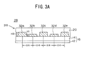
- FIGS. 3A and 3B A description will now be given, with reference to FIGS. 3A and 3B, of a structure of a printed circuit board 28 according to a second embodiment of the present invention.
- FIG. 3A is a partial cross-sectional view of the printed circuit board 28 , on which a plurality of wiring lines 32 a through 32 e are arranged, showing a region of narrow wiring pattern pitches.
- FIG. 3B is a partial perspective view of the wiring lines 32 a and 32 b including the portions thereof of which the cross sections are shown in FIG. 3 A.
- the wiring lines 32 a through 32 e are arranged on the board 16 with the pattern pitches X 4 , which is described in the first embodiment, in a region 310 .
- the wiring lines 32 a , 32 c , and 32 e has a thickness H 3 which corresponds to the thickness H 1 - 1 or H 2 - 1 described in the first embodiment, and the wiring lines 32 b and 32 d has the thickness H 1 described in the first embodiment, which is thinner than the thickness H 3 .
- the wiring line 32 b is formed to have a portion of the thinner thickness H 1 (or a first portion) in the region 310 compared with the other wiring lines 32 a , 32 c , and 32 e.
- the wiring lines 32 b and 32 d are laid out between the wiring lines 32 a and 32 c , and between the wiring lines 32 c and 32 e , respectively, so that each of the wiring lines having the thickness H 3 will be placed adjacently to each of the wiring lines having the thickness H 1 .
- the area Sm of the overlapping part of the facing surfaces of the wiring line 32 a (or a second wiring line) and the wiring line 32 b (or a first wiring line) per unit length is smaller than that of the overlapping part of the facing surfaces of wiring lines of the thickness H 3 per unit length which are laid out with the pattern pitch X 4 (See FIG. 3 B).
- a mutual capacitance between the adjacent wiring lines 32 a and 32 b is smaller than that between the above wiring lines of the thickness H 3 per unit length which are laid out with the pattern pitch X 4 , making the value of K obtained from the above formula a desired small value.
- the other pairs of the adjacent wiring lines shown in FIG. 3 A are the same holds true for the other pairs of the adjacent wiring lines shown in FIG. 3 A.
- the noise level of a crosstalk noise generated between adjacent two of the wiring lines is lowered to the extent that no problem is incurred.
- FIG. 4 is a partial cross-sectional view of a printed circuit board 100 showing a region wherein wiring lines are laid out with extremely narrow pattern pitches according to a third embodiment of the present invention.
- Wiring lines 104 a through 104 e correspond, for example, to the wiring lines 26 c and 26 d of the first embodiment, and are arranged on the board 16 with extremely narrower pattern pitches X 5 than the pattern pitch X 4 of the first embodiment.
- a wiring line L having the thickness H 3 described in the second embodiment is shown by dotted lines over the wiring line 104 a in FIG. 4 .
- the wiring line 104 a is formed by trimming off both shoulder portions of a wiring line having the thickness H 4 slightly thinner than the wiring line L so as to have a triangular cross-sectional shape with slopes 104 a 1 and 104 a 2 .
- the thickness H 4 between the surface of the board 16 and a top portion 104 a 3 of the wiring line 104 a is thinner than the thickness H 3 .
- the other wiring lines 104 b through 104 e have the same cross-sectional shape and slopes as the above described wiring line 104 a.
- the adjacent wiring lines 104 a and 104 b are laid out with the slope 104 a 2 and a slope 104 b 1 facing each other to form a V shape between the wiring lines 104 a and 104 b . Therefore, a distance dm between the slopes 104 a 2 and 104 b 1 gradually extends toward the top portion 104 a 3 and a top portion 104 b 3 .
- a mutual capacitance between the adjacent wiring lines 104 a and 104 b is smaller than that between adjacent wiring lines having rectangular cross-sectional shapes which are laid out with the pattern pitch X 5 , making the value of K obtained from the above formula a desired value small enough to lower the noise level of the crosstalk noise between the wiring lines 104 a and 104 b to the extent that no problem is incurred.
- the level of a crosstalk noise generated between adjacent two of the wiring lines is lowered to the extent that no problem is incurred.
- the thickness H 4 between the surface of the board 16 and the top portion 104 a 3 of the wiring line 104 a may be set as thick as or slightly thicker than the thickness H 3 as far as the value of K is maintained to the desired small value.
- the wiring lines 104 a through 104 e can easily be formed only by trimming off both shoulder portions of the wiring line L without changing the thickness.
- each of the wiring lines 104 a through 104 e may be formed so as to have a trapezoidal cross-sectional shape of which an upper side is shorter than a lower side thereof remaining in contact with the surface of the board 16 , instead of the triangular cross-sectional shape.
- a board 38 including a core layer 36 formed on a GND layer should first be prepared.
- a conductive paste made of a conductive material is applied on the board 38 so as to form a conductive paste layer 40 thereon.
- a mask 42 is placed on the conductive paste layer 40 so as to form a wiring pattern thereon.
- the conductive paste layer 40 is etched so that wiring lines 44 a through 44 d will be formed according to the wiring pattern as shown in FIG. 2 B. In this case, every wiring line is formed so as to have a uniform thickness H 6 .
- each of the wiring lines 44 c and 44 d is etched, after the etching liquid is sprayed thereon, to have a thickness H 7 , which is thinner than the thickness H 6 , as shown in FIG. 5 D.
- a printed circuit board 48 on which the wiring lines 44 a and 44 b , each having the thickness H 6 , are formed with a pattern pitch X 9 , and the wiring lines 44 c and 44 d , each having the thickness H 7 , are formed with a pattern pitch X 10 , which is narrower than the pattern pitch X 9 .
- the wiring lines 44 a through 44 d may be referred to as a first through a fourth wiring line, respectively.
- the printed circuit board 48 of the present invention may properly be formed.
- a mask 52 is first placed on a core layer 50 so as to form a wiring pattern thereon. Then, a conductive paste made of a conductive material is applied, or evaporated on unmasked portions of the core layer 50 to form wiring lines 54 a through 54 d according to the wiring pattern as shown in FIG. 6 B. In this case, every wiring line is formed to have a uniform thickness H 8 .
- a mask 56 is provided so that only the wiring lines 54 a and 54 b will be unmasked as shown in FIG. 6 C. Then, the conductive paste made of the conductive material is applied, or evaporated on the wiring lines 54 a and 54 b so that the wiring lines 54 a and 54 b will be formed to have a thickness H 9 , which is thicker than the thickness H 8 , as shown in FIG. 6 D.
- a printed circuit board 55 on which the wiring lines 54 a and 54 b , each having the thickness H 9 , are formed with a pattern pitch X 1 , and the wiring lines 54 c and 54 d , each having the thickness H 8 , are formed with a pattern pitch X 12 , which is narrower than the pattern pitch X 11 .
- the wiring lines 54 a through 54 d may be referred to as a first through a fourth wiring line, respectively.
- the printed circuit board 55 of the present invention may properly be formed as in the case of the above method of forming the wiring lines on the board to form the printed circuit board according to the fourth embodiment of the present invention.
- wiring lines 58 a through 58 d are formed according to a wiring pattern on a core layer 57 in the same method as described in the above embodiments of the present invention. In this case, every wiring line is formed to have a uniform thickness H 10 .
- each of only the wiring lines 58 C and 58 D is ground by using a mask or a template to have a thickness H 11 , which is thinner than the thickness H 10 , as shown in FIG. 7 B.
- a printed circuit board 60 on which the wiring lines 58 a and 58 b , each having the thickness H 10 , are formed with a pattern pitch X 13 , and the wiring lines 58 c and 58 d , each having the thickness H 11 , are formed with a pattern pitch X 14 , which is narrower than the pattern pitch X 13 .
- the wiring lines 58 a through 58 d may be referred to as a first through a fourth wiring line, respectively.
- the printed circuit board 60 of the present invention may properly be formed as in the case of the above method of forming the wiring lines on the board to form the printed circuit board according to the fourth embodiment of the present invention.
- FIGS. 8A through 8E A description will now be given of a method of forming wiring lines on a board to form a printed circuit board according to a seventh embodiment of the present invention with reference to FIGS. 8A through 8E.
- the wiring lines of the printed circuit board 100 shown in FIG. 4 are formed.
- a conductive paste made of a conductive material is applied on the board 16 to form a conductive paste layer 110 thereon, and a mask 120 is placed on the conductive paste layer 110 so as to form a wiring pattern thereon as shown in FIG. 8 A.
- the conductive paste layer 110 is etched according to the wiring pattern so as to form wiring lines 111 a through 111 c , each having the thickness H 2 shown in FIG. 2B, with the pattern pitches X 4 shown in FIG. 4 .
- a mask 121 is provided so as to etch both shoulder portions of each of the wiring lines 111 a through 111 c .
- portions between the adjacent two of the wiring lines 111 a through 111 c , and a center portion along a longitudinal center line of a top surface of each of the wiring lines 111 a through 111 c are masked, while the rest of the top surface of each of the wiring lines 111 a through 111 c , which corresponds to top surfaces of both of the shoulder portions thereof, remains unmasked.
- an etching process is performed for a predetermined period of time so that both of the shoulder portions of each of the wiring lines 111 a through 111 c will be etched, having undercuts around a top longitudinal center portion thereof.
- a printed circuit board 70 on which the wiring lines 111 a through 111 c , each having the thickness H 2 and the triangular cross-sectional shape, are formed with the pattern pitches X 5 .
- the printed circuit board 70 of the present invention may properly be formed as in the case of the above method of forming the wiring lines on the board to form the printed circuit board according to the fourth embodiment of the present invention.
Landscapes
- Engineering & Computer Science (AREA)
- Microelectronics & Electronic Packaging (AREA)
- Manufacturing & Machinery (AREA)
- Physics & Mathematics (AREA)
- Electromagnetism (AREA)
- Structure Of Printed Boards (AREA)
Abstract
A printed circuit board includes a first wiring line and a second wiring line spaced apart from the first wiring line. The first wiring line has a first portion having a surface which faces the second wiring line and is smaller in area than that of the second portion, so that a crosstalk noise between the first portion of the first wiring line and the second wiring line can be reduced.
Description
1. Field of the Invention
The present invention generally relates to printed circuit boards and methods of forming wiring lines on boards to form such printed circuit boards, and more particularly, to a printed circuit board with reduced crosstalk noise generated between adjacent two of a plurality of wiring lines spaced thereon, and a method of forming wiring lines on a board to form such a printed circuit board.
2. Description of the Related Art
A plurality of wiring lines and electronic components are disposed on a printed circuit board, so that a crosstalk noise will be generated between adjacent two of the wiring lines which are not sufficiently spaced. Here, the term “crosstalk noise” refers to a noise which is generated when a signal conducted through a signal (wiring) line is induced by an adjacent signal (wiring) line because of a coupling caused by a mutual capacitance or inductance between the adjacent signal (wiring) lines. When a high-frequency clock pulse is employed as a signal, the problem of false operation caused by such a crosstalk noise will surface.
For example, according to a wiring layout on a printed circuit board 1 shown in FIG. 1, a plurality of LSIs 2 a, 2 b, and 2 c are connected by means of a plurality of wiring lines. In FIG. 1, adjacent two of the wiring lines are laid out at a distance X1 from each other in a region 150, adjacent two of the wiring lines which are disposed so as to bypass electronic components 3 a and 3 b are laid out at a distance X2-1 from each other in a region 160, and adjacent two of the wiring lines which are disposed with high density are laid out at a distance X2-2 from each other in a region 170.
Herein, the distance X1 is longer than the distances X2-1 and X2-2. Therefore, the noise level of a crosstalk noise generated between the adjacent two of the wiring lines laid out in the region 150 is higher than those generated between the adjacent two of the wiring lines laid out in the region 160 and between the adjacent two of the wiring lines laid out in the region 170.
In order to avoid the above drawback, a change in the wiring layout is generally made so as to lengthen the distances X2-1 and X2-2, which in turn, requires a greater wiring region or multiple wiring layers.
Hereinafter, a distance between two adjacent wiring lines is referred to as a pattern pitch.
It is a general object of the present invention to provide a printed circuit board and a method of forming wiring lines on a board to form such a printed circuit board in which the above disadvantages are eliminated.
A more specific object of the present invention is to provide a high-density printed circuit board with reduced crosstalk noise and a method of forming wiring lines on a board to form such a printed circuit board.
The above objects of the present invention are achieved by a printed circuit board including a first wiring line and a second wiring line spaced apart from the first wiring line, wherein the first wiring line has first and second portions, the first portion having a surface which faces the second wiring line and is smaller in area than that of the second portion.
The above objects of the present invention are achieved by a printed circuit board including a first wiring line and a second wiring line spaced apart from the first wiring line, wherein the first wiring line has a first portion having a surface which faces the second wiring line and is smaller in area than a surface of the second wiring line which faces the first portion of the first wiring line.
According to the above structures, the area of the overlapping part of the facing surfaces of adjacent two of wiring lines per unit length of a wiring line can be reduced so as to reduce a crosstalk noise between the adjacent two wiring lines.
The above objects of the present invention are also achieved by a method of forming wiring lines on a board to form a printed circuit board including the steps of forming the wiring lines of a predetermined uniform thickness, and etching a first wiring line thereof so that the first wiring line has a first portion thinner than a second portion thereof.
The above objects of the present invention are also achieved by a method of forming wiring lines on a board to form a printed circuit board including the steps of forming the wiring lines of a predetermined uniform thickness, and applying a conductive material on a first wiring line thereof so that the first wiring line has a first portion thicker than a second portion thereof.
The above objects of the present invention are also achieved by a method of forming wiring lines on a board to form a printed circuit board including the steps of forming the wiring lines of a predetermined uniform thickness, and grinding a first wiring line thereof so that the first wiring line has a first portion thinner than a second portion thereof.
According to the above methods, the printed circuit boards of the present invention may properly be formed.
Other objects, features and advantages of the present invention will become more apparent from the following detailed description when read in conjunction with the accompanying drawings, in which:
FIG. 1 is a diagram showing a conventional wiring layout on a printed circuit board;
FIG. 2A is a partial cross-sectional view of a printed circuit board according to a first embodiment of the present invention;
FIGS. 2B and 2C are partial perspective views of wiring lines formed on the printed circuit board of FIG. 2A;
FIG. 3A is a partial cross-sectional view of a printed circuit board according to a second embodiment of the present invention;
FIG. 3B is a partial perspective view of wiring lines formed on the printed circuit board of FIG. 3A;
FIG. 4 is a partial cross-sectional view of a printed circuit board according to a third embodiment of the present invention;
FIGS. 5A through 5D are diagrams illustrating a method of forming wiring lines on a board to firm a printed circuit board according to a fourth embodiment of the present invention;
FIGS. 6A through 6D are diagrams illustrating a method of forming wiring lines on a board to form a printed circuit board according to a fifth embodiment of the present invention;
FIGS. 7A and 7B are diagrams illustrating a method of forming wiring lines on a board to form a printed circuit board according to a sixth embodiment of the present invention; and
FIGS. 8A through 8E are diagrams illustrating a method of forming wiring lines on a board to form a printed circuit board according to a seventh embodiment of the present invention.
In the following, embodiments of the present invention will be described with reference to the accompanying drawings.
A description will first be given of a formula to calculate a coefficient K which indicates the amplitude of a crosstalk noise. The noise level of the crosstalk noise generated in any portion of a printed circuit board can be estimated by using the following formula. As the coefficient K becomes greater, the level of the crosstalk noise becomes higher.
In the above formula, K is the coefficient to indicate the amplitude of the crosstalk noise, Lm is a mutual inductance between two adjacent wiring lines per unit length of a wiring line (unit: H), Lo is an inductance of one of the two adjacent wiring lines per unit length of a wiring line (unit: H), Cm is a mutual capacitance between the two adjacent wiring lines per unit length of a wiring line (unit: F), Co is a capacitance of one of the two adjacent wiring lines per unit length of a wiring line (unit: F), Td is a propagation delay time per unit length of a wiring line (unit: m/s), 1 is a length of a coupled portion of one of the two adjacent wiring lines (unit: m), V is the amplitude of a signal source (unit: V), and t is time (unit: s).
Further, Cm is given as Cm=∈×Sm/dm, wherein ∈ is the dielectric constant of an insulator between the two adjacent wiring lines, Sm is the area of the overlapping part of the surfaces facing each other, or facing surfaces, of the two adjacent wiring lines per unit length of a wiring line, and dm is a distance between the facing surfaces of the two adjacent wiring lines. Moreover, Co is given as Co=∈×So/do, wherein {dot over (a)} is the dielectric constant of an insulator between the two adjacent wiring lines and a GND (ground) layer, So is the area of the overlapping part of the facing surfaces of one of the two adjacent wiring lines and the GND layer, and do is a distance between one of the two adjacent wiring lines and the GND layer.
In the present invention, according to the above formula, the value of K can be reduced, so as to lower the noise level of a crosstalk noise, by reducing Lm and Cm by setting the area Sm required to set the level of the crosstalk noise to a level equal to or lower than a desired level when other values such as dm, ∈, and So cannot be changed, that is, Lo and Co remain constant.
A description will now be given, with reference to FIGS. 2A through 2C, of a structure of a printed circuit board 22 according to a first embodiment of the present invention.
FIG. 2A is a partial cross-sectional view of the printed circuit board 22 showing surrounding areas of a boundary between a region of a wide wiring pattern pitch and a region of a narrow wiring pattern pitch.
The printed circuit board 22 includes a board 16 having a GND layer 12 made of a conductive material, and a core layer 14 made of a dielectric material stacked on the GND layer 12. A plurality of wiring lines 26 a through 26 d (or a third, a fourth, a first, and a second wiring line, respectively) made of a conductive material are disposed on the board 16, being covered with a prepreg layer 20 made of a dielectric material.
FIG. 2B is a partial perspective view of the wiring lines 26 a and 26 b including the portions thereof of which the cross sections are shown in FIG. 2A. FIG. 2C is a partial perspective view of the wiring lines 26 c and 26 d including the portions thereof of which the cross sections are shown in FIG. 2A.
As shown in FIG. 2B, the wiring lines 26 a and 26 b have portions of a height H2 in a region 210 (or a first and a third portion, respectively) and portions of a height H2-1 in a region 220 (or a second and a fourth portion, respectively). As shown in FIG. 2C, the wiring lines 26 c and 26 d have portions of a height H1 in a region 230 (or a first and a third portion, respectively) and portions of a height H1-1 in a region 240 (or a second and a fourth portion, respectively).
The wiring lines 26 a and 26 b, as shown in FIG. 2B, have a wider pattern pitch X3 therebetween in the region 210 than a pattern pitch X3-1 therebetween in the region 220. On the other hand, the wiring lines 26 c and 26 d, as shown in FIG. 2C, have a narrower pattern pitch X4 therebetween in the region 230 than a pattern pitch X4-1 therebetween in the region 240 as the wiring lines 26 c and 26 d are laid out with high density because of the wiring layout restricted by a plurality of wiring lines and electronic components disposed on the board 16 (see FIG. 1).
The thickness H1 of the wiring lines 26 c and 26 d laid out with the pattern pitch X4 in the region 230 is thinner than the thickness H1-1 of the wiring lines 26 c and 26 d laid out with the pattern pitch X4-1 in the region 240. This is because the noise level of a crosstalk noise between the wiring lines 26 c and 26 d is estimated from the above described formula to calculate K to be improperly higher in the region 230 than in the region 240 because of the narrow pattern pitch X4 according to the wiring layout if the thickness of the wiring lines 26 c and 26 d remain the thickness H1-1. Accordingly, the thickness H1 is set so as to obtain a desired value of K indicating a desired low noise level of the crosstalk noise therebetween in the region 230, thus allowing a high-density wiring layout therein.
On the other hand, the thickness H2 of the wiring lines 26 a and 26 b laid out with the pattern pitch X3 in the region 210 is thicker than the thickness H2-1 of the wiring lines 26 a and 26 b laid out with the pattern pitch X3-1 in the region 220. This is because the noise level of a crosstalk noise between the wiring lines 26 a and 26 b is estimated from the above described formula to be lower in the region 210 than in the region 220 because of the wide pattern pitch X3 according to the wiring layout if the thickness of the wiring lines 26 a and 26 b remain the thickness H2-1. Accordingly, the thickness H2 is set within a given range so that the noise level of the crosstalk noise will not become improperly high. The thickness H1-1 is equal to the thickness H2-1 since wiring lines are usually formed so as to have the same thickness.
According to the printed circuit board 22 having the above structure, the area Sm of the overlapping part of the facing surfaces of the wiring lines 26 c and 26 d per unit length is smaller in the region 230 than in the region 240. This is because the wiring lines 26 c and 26 d each have the thinner thickness H1-1 in the region 230 than the thickness H1-1 in the region 240. Therefore, a mutual capacitance between the wiring lines 26 c and 26 d per unit length in the region 230 is smaller than that between wiring lines of the thickness H1-1 per unit length which are laid out with the pattern pitch X4. Thus, the value of K obtained from the above formula becomes a desired value small enough to lower the noise level of the crosstalk noise between the wiring lines 26 c and 26 d in the region 230 to the extent that no problem is incurred.
If the pattern pitch X4 is replaced with the pattern pitch X4-1 between the wiring lines 26 c and 26 d in the region 230 in the above case, the crosstalk noise therebetween will further be reduced.
On the other hand, the wiring lines 26 a and 26 b are laid out with the wider pattern pitch X3 in the region 210 than the pattern pitch X3-1 in the region 220, and have the thicker thickness H2 in the region 210 than the thickness H2-1 in the region 220. Therefore, when the wiring lines 26 a through 26 d are connected to make a continuous circuit, for example, increases in the resistances of the thinner portions, or the first and third portions, respectively, of the wiring lines 26 c and 26 d in the region 230 are offset by decreases in the resistances of the thicker portions, or the first and third portions, respectively, of the wiring lines 26 a and 26 b in the region 210. In this case, the pattern pitch X3 may also be set as short as the pattern pitch X3-1 in the region 210 with the thickness H2 being replaced with the thickness H2-1, thus allowing a high density wiring layout in the region 210.
The above will become clearer when the wiring lines 26 a and 26 c are different portions of the same wiring line, and the wiring lines 26 b and 26 d are different portions of the same wiring line.
A description will now be given, with reference to FIGS. 3A and 3B, of a structure of a printed circuit board 28 according to a second embodiment of the present invention.
FIG. 3A is a partial cross-sectional view of the printed circuit board 28, on which a plurality of wiring lines 32 a through 32 e are arranged, showing a region of narrow wiring pattern pitches. FIG. 3B is a partial perspective view of the wiring lines 32 a and 32 b including the portions thereof of which the cross sections are shown in FIG. 3A.
As shown in FIG. 3A, the wiring lines 32 a through 32 e are arranged on the board 16 with the pattern pitches X4, which is described in the first embodiment, in a region 310. The wiring lines 32 a, 32 c, and 32 e has a thickness H3 which corresponds to the thickness H1-1 or H2-1 described in the first embodiment, and the wiring lines 32 b and 32 d has the thickness H1 described in the first embodiment, which is thinner than the thickness H3. That is, the wiring line 32 b, as well as the wiring line 32 d, is formed to have a portion of the thinner thickness H1 (or a first portion) in the region 310 compared with the other wiring lines 32 a, 32 c, and 32 e.
The wiring lines 32 b and 32 d are laid out between the wiring lines 32 a and 32 c, and between the wiring lines 32 c and 32 e, respectively, so that each of the wiring lines having the thickness H3 will be placed adjacently to each of the wiring lines having the thickness H1.
Therefore, for example, the area Sm of the overlapping part of the facing surfaces of the wiring line 32 a (or a second wiring line) and the wiring line 32 b (or a first wiring line) per unit length is smaller than that of the overlapping part of the facing surfaces of wiring lines of the thickness H3 per unit length which are laid out with the pattern pitch X4 (See FIG. 3B). Thus, a mutual capacitance between the adjacent wiring lines 32 a and 32 b is smaller than that between the above wiring lines of the thickness H3 per unit length which are laid out with the pattern pitch X4, making the value of K obtained from the above formula a desired small value. The same holds true for the other pairs of the adjacent wiring lines shown in FIG. 3A.
According to the printed circuit board 28 having the above structure, in a region wherein wiring lines are laid out with the pattern pitches X4, the noise level of a crosstalk noise generated between adjacent two of the wiring lines is lowered to the extent that no problem is incurred.
FIG. 4 is a partial cross-sectional view of a printed circuit board 100 showing a region wherein wiring lines are laid out with extremely narrow pattern pitches according to a third embodiment of the present invention.
Wiring lines 104 a through 104 e correspond, for example, to the wiring lines 26 c and 26 d of the first embodiment, and are arranged on the board 16 with extremely narrower pattern pitches X5 than the pattern pitch X4 of the first embodiment. For the convenience of a description, a wiring line L having the thickness H3 described in the second embodiment is shown by dotted lines over the wiring line 104 a in FIG. 4. In this case, the wiring line 104 a is formed by trimming off both shoulder portions of a wiring line having the thickness H4 slightly thinner than the wiring line L so as to have a triangular cross-sectional shape with slopes 104 a 1 and 104 a 2. Therefore, the thickness H4 between the surface of the board 16 and a top portion 104 a 3 of the wiring line 104 a is thinner than the thickness H3. The other wiring lines 104 b through 104 e have the same cross-sectional shape and slopes as the above described wiring line 104 a.
The adjacent wiring lines 104 a and 104 b are laid out with the slope 104 a 2 and a slope 104 b 1 facing each other to form a V shape between the wiring lines 104 a and 104 b. Therefore, a distance dm between the slopes 104 a 2 and 104 b 1 gradually extends toward the top portion 104 a 3 and a top portion 104 b 3. Thus, a mutual capacitance between the adjacent wiring lines 104 a and 104 b is smaller than that between adjacent wiring lines having rectangular cross-sectional shapes which are laid out with the pattern pitch X5, making the value of K obtained from the above formula a desired value small enough to lower the noise level of the crosstalk noise between the wiring lines 104 a and 104 b to the extent that no problem is incurred. The same holds true for the other pairs of the adjacent wiring lines shown in FIG. 4.
According to the printed circuit board 100 having the above structure according to the third embodiment of the present invention, in a region wherein wiring lines are laid out with the pattern pitches X5, the level of a crosstalk noise generated between adjacent two of the wiring lines is lowered to the extent that no problem is incurred.
In this case, the thickness H4 between the surface of the board 16 and the top portion 104 a 3 of the wiring line 104 a may be set as thick as or slightly thicker than the thickness H3 as far as the value of K is maintained to the desired small value. When the thickness H4 is set as thick as the thickness H3 in the above case, the wiring lines 104 a through 104 e can easily be formed only by trimming off both shoulder portions of the wiring line L without changing the thickness. Further, each of the wiring lines 104 a through 104 e may be formed so as to have a trapezoidal cross-sectional shape of which an upper side is shorter than a lower side thereof remaining in contact with the surface of the board 16, instead of the triangular cross-sectional shape.
A description will now be given of a method of forming wiring lines on a board to form a printed circuit board according to a fourth embodiment of the present invention with reference to FIGS. 5A through 5D.
First, a board 38 including a core layer 36 formed on a GND layer (not shown) should first be prepared. Next, as shown in FIG. 5A, a conductive paste made of a conductive material is applied on the board 38 so as to form a conductive paste layer 40 thereon. Then, a mask 42 is placed on the conductive paste layer 40 so as to form a wiring pattern thereon.
Next, after an etching liquid or etchant is sprayed on unmasked portions of the conductive paste layer 40, the conductive paste layer 40 is etched so that wiring lines 44 a through 44 d will be formed according to the wiring pattern as shown in FIG. 2B. In this case, every wiring line is formed so as to have a uniform thickness H6.
Then, a mask 46 is provided so that only the wiring lines 44 c and 44 d will be unmasked as shown in FIG. 5C. Then, each of the wiring lines 44 c and 44 d is etched, after the etching liquid is sprayed thereon, to have a thickness H7, which is thinner than the thickness H6, as shown in FIG. 5D.
Thereby, formed is a printed circuit board 48 on which the wiring lines 44 a and 44 b, each having the thickness H6, are formed with a pattern pitch X9, and the wiring lines 44 c and 44 d, each having the thickness H7, are formed with a pattern pitch X10, which is narrower than the pattern pitch X9. Herein, the wiring lines 44 a through 44 d may be referred to as a first through a fourth wiring line, respectively.
According to the above method of forming the wiring lines on the board to form the printed circuit board according to the fourth embodiment of the present invention, the printed circuit board 48 of the present invention may properly be formed.
A description will now be given of a method of forming wiring lines on a board to form a printed circuit board according to a fifth embodiment of the present invention with reference to FIGS. 6A through 6D.
As shown in FIG. 6A, a mask 52 is first placed on a core layer 50 so as to form a wiring pattern thereon. Then, a conductive paste made of a conductive material is applied, or evaporated on unmasked portions of the core layer 50 to form wiring lines 54 a through 54 d according to the wiring pattern as shown in FIG. 6B. In this case, every wiring line is formed to have a uniform thickness H8.
Next, a mask 56 is provided so that only the wiring lines 54 a and 54 b will be unmasked as shown in FIG. 6C. Then, the conductive paste made of the conductive material is applied, or evaporated on the wiring lines 54 a and 54 b so that the wiring lines 54 a and 54 b will be formed to have a thickness H9, which is thicker than the thickness H8, as shown in FIG. 6D.
Thereby, formed is a printed circuit board 55 on which the wiring lines 54 a and 54 b, each having the thickness H9, are formed with a pattern pitch X1, and the wiring lines 54 c and 54 d, each having the thickness H8, are formed with a pattern pitch X12, which is narrower than the pattern pitch X11. Herein, the wiring lines 54 a through 54 d may be referred to as a first through a fourth wiring line, respectively.
According to the above method of forming the wiring lines on the board to form the printed circuit board according to the fifth embodiment of the present invention, the printed circuit board 55 of the present invention may properly be formed as in the case of the above method of forming the wiring lines on the board to form the printed circuit board according to the fourth embodiment of the present invention.
A description will now be given of a method of forming wiring lines on a board to form a printed circuit board according to a sixth embodiment of the present invention with reference to FIGS. 7A and 7B.
First, as shown in FIG. 7A, wiring lines 58 a through 58 d are formed according to a wiring pattern on a core layer 57 in the same method as described in the above embodiments of the present invention. In this case, every wiring line is formed to have a uniform thickness H10.
Next, each of only the wiring lines 58C and 58D is ground by using a mask or a template to have a thickness H11, which is thinner than the thickness H10, as shown in FIG. 7B.
Thereby, formed is a printed circuit board 60 on which the wiring lines 58 a and 58 b, each having the thickness H10, are formed with a pattern pitch X13, and the wiring lines 58 c and 58 d, each having the thickness H11, are formed with a pattern pitch X14, which is narrower than the pattern pitch X13. Herein, the wiring lines 58 a through 58 d may be referred to as a first through a fourth wiring line, respectively.
According to the above method of forming the wiring lines on the board to form the printed circuit board according to the sixth embodiment of the present invention, the printed circuit board 60 of the present invention may properly be formed as in the case of the above method of forming the wiring lines on the board to form the printed circuit board according to the fourth embodiment of the present invention.
A description will now be given of a method of forming wiring lines on a board to form a printed circuit board according to a seventh embodiment of the present invention with reference to FIGS. 8A through 8E.
In this method, the wiring lines of the printed circuit board 100 shown in FIG. 4 are formed.
First, a conductive paste made of a conductive material is applied on the board 16 to form a conductive paste layer 110 thereon, and a mask 120 is placed on the conductive paste layer 110 so as to form a wiring pattern thereon as shown in FIG. 8A.
Next, as shown in FIG. 8B, the conductive paste layer 110 is etched according to the wiring pattern so as to form wiring lines 111 a through 111 c, each having the thickness H2 shown in FIG. 2B, with the pattern pitches X4 shown in FIG. 4.
Next, as shown in FIG. 8C, a mask 121 is provided so as to etch both shoulder portions of each of the wiring lines 111 a through 111 c. With the mask 121 being provided, portions between the adjacent two of the wiring lines 111 a through 111 c, and a center portion along a longitudinal center line of a top surface of each of the wiring lines 111 a through 111 c are masked, while the rest of the top surface of each of the wiring lines 111 a through 111 c, which corresponds to top surfaces of both of the shoulder portions thereof, remains unmasked.
Then, as shown in FIG. 8D, an etching process is performed for a predetermined period of time so that both of the shoulder portions of each of the wiring lines 111 a through 111 c will be etched, having undercuts around a top longitudinal center portion thereof.
Thereby, as shown in FIG. 8E, formed is a printed circuit board 70 on which the wiring lines 111 a through 111 c, each having the thickness H2 and the triangular cross-sectional shape, are formed with the pattern pitches X5.
According to the above method of forming the wiring lines on the board to form the printed circuit board according to the seventh embodiment of the present invention, the printed circuit board 70 of the present invention may properly be formed as in the case of the above method of forming the wiring lines on the board to form the printed circuit board according to the fourth embodiment of the present invention.
The present invention is not limited to the specifically disclosed embodiments, and variations and modifications may be made without departing from the scope of the present invention.
The present application is based on Japanese priority application No. 11-340815 filed on Nov. 30, 1999, the entire contents of which are hereby incorporated by reference.
Claims (30)
1. A printed circuit board comprising:
a first wiring line; and
a second wiring line spaced apart from the first wiring line,
the first wiring line having first and second portions, the first portion having a surface which faces the second wiring line and is smaller in area than that of the second portion, so that a crosstalk noise between the first portion of the first wiring line and the second wiring line can be reduced.
2. The printed circuit board as claimed in claim 1 , wherein the second wiring line has third and fourth portions, the third portion having a surface which faces the first wiring line and is smaller in area than that of the fourth portion, so that a crosstalk noise between the third portion of the second wiring line and the first wiring line can be reduced.
3. The printed circuit board as claimed in claim 1 , wherein the first portion of the first wiring line is thinner than the second portion thereof.
4. The printed circuit board as claimed in claim 1 , wherein the first portion of the first wiring line has a triangular cross-sectional shape.
5. The printed circuit board as claimed in claim 1 , wherein the first portion of the first wiring line has a trapezoidal cross-sectional shape.
6. The printed circuit board as claimed in claim 2 , wherein the first portion of the first wiring line is thinner than the second portion thereof, and the third portion of the second wiring line is thinner than the fourth portion thereof.
7. The printed circuit board as claimed in claim 6 , wherein the first portion of the first wiring line and the third portion of the second wiring line have an identical height.
8. The printed circuit board as claimed in claim 7 , wherein the first portion of the first wiring line faces the third portion of the second wiring line.
9. The printed circuit board as claimed in claim 7 , wherein:
the first portion of the first wiring line faces the third portion of the second wiring line;
the second portion of the first wiring line faces the fourth portion of the second wiring line; and
a distance between the first and third portions is shorter than that between the second and fourth portions.
10. The printed circuit board as claimed in claim 6 , wherein the first portion of the first wiring line faces the third portion of the second wiring line.
11. The printed circuit board as claimed in claim 6 , wherein:
the first portion of the first wiring line faces the third portion of the second wiring line;
the second portion of the first wiring line faces the fourth portion of the second wiring line; and
a distance between the first and third portions is shorter than that between the second and fourth portions.
12. The printed circuit board as claimed in claim 2 , wherein the first portion of the first wiring line and the third portion of the second wiring line have a triangular cross-sectional shape.
13. The printed circuit board as claimed in claim 12 , wherein the first portion of the first wiring line and the third portion of the second wiring line have an identical height.
14. The printed circuit board as claimed in claim 13 , wherein the first portion of the first wiring line faces the third portion of the second wiring line.
15. The printed circuit board as claimed in claim 12 , wherein the first portion of the first wiring line faces the third portion of the second wiring line.
16. The printed circuit board as claimed in claim 2 , wherein the first portion of the first wiring line and the third portion of the second wiring line have a trapezoidal cross-sectional shape.
17. The printed circuit board as claimed in claim 16 , wherein the first portion of the first wiring line and the third portion of the second wiring line have an identical height.
18. The printed circuit board as claimed in claim 17 , wherein the first portion of the first wiring line faces the third portion of the second wiring line.
19. The printed circuit board as claimed in claim 16 , wherein the first portion of the first wiring line faces the third portion of the second wiring line.
20. The printed circuit board as claimed in claim 1 , further comprising:
a third wiring line; and
a fourth wiring line spaced apart from the third wiring line,
the third wiring line having first and second portions, the first portion having a surface which faces the fourth wiring line and is larger in area than that of the second portion.
21. The printed circuit board as claimed in claim 20 , wherein the fourth wiring line has third and fourth portions, the third portion having a surface which faces the third wiring line and is larger in area than that of the fourth portion.
22. The printed circuit board as claimed in claim 21 , wherein the first portion of the third wiring line is thicker than the second portion thereof, and the third portion of the fourth wiring line is thicker than the fourth portion thereof.
23. The printed circuit board as claimed in claim 22 , wherein the first portion of the third wiring line and the third portion of the fourth wiring line have an identical height.
24. The printed circuit board as claimed in claim 23 , wherein the first portion of the third wiring line faces the third portion of the fourth wiring line.
25. The printed circuit board as claimed in claim 20 , wherein the first portion of the third wiring line is thicker than the second portion thereof.
26. The printed circuit board as claimed in claim 22 , wherein the first portion of the third wiring line faces the third portion of the fourth wiring line.
27. A printed circuit board comprising:
a first wiring line; and
a second wiring line spaced apart from the first wiring line,
the first wiring line including a first portion having a surface which faces the second wiring line and is smaller in area than a surface of the second wiring line which faces the first portion of the first wiring line, so that a crosstalk noise between the first portion of the first wiring line and the second wiring line can be reduced.
28. The printed circuit board as claimed in claim 27 , wherein the first portion of the first wiring line is thinner than the second wiring line.
29. The printed circuit board as claimed in claim 27 , further comprising:
a third wiring line; and
a fourth wiring line spaced apart from the first wiring line,
the third wiring line including a first portion having a surface which faces the fourth wiring line and is larger in area than a surface of the fourth wiring line which faces the first portion of the third wiring line.
30. The printed circuit board as claimed in claim 29 , wherein the first portion of the third wiring line is thicker than the fourth wiring line.
Priority Applications (1)
| Application Number | Priority Date | Filing Date | Title |
|---|---|---|---|
| US09/928,441 US20020027021A1 (en) | 1999-11-30 | 2001-08-14 | Printed circuit board with reduced crosstalk noise and method of forming wiring lines on a board to form such a printed circuit board |
Applications Claiming Priority (2)
| Application Number | Priority Date | Filing Date | Title |
|---|---|---|---|
| JP34081599A JP2001156408A (en) | 1999-11-30 | 1999-11-30 | Printed circuit board and wiring forming method |
| JP11-340815 | 1999-11-30 |
Related Child Applications (1)
| Application Number | Title | Priority Date | Filing Date |
|---|---|---|---|
| US09/928,441 Division US20020027021A1 (en) | 1999-11-30 | 2001-08-14 | Printed circuit board with reduced crosstalk noise and method of forming wiring lines on a board to form such a printed circuit board |
Publications (1)
| Publication Number | Publication Date |
|---|---|
| US6340798B1 true US6340798B1 (en) | 2002-01-22 |
Family
ID=18340557
Family Applications (2)
| Application Number | Title | Priority Date | Filing Date |
|---|---|---|---|
| US09/630,685 Expired - Fee Related US6340798B1 (en) | 1999-11-30 | 2000-08-01 | Printed circuit board with reduced crosstalk noise and method of forming wiring lines on a board to form such a printed circuit board |
| US09/928,441 Abandoned US20020027021A1 (en) | 1999-11-30 | 2001-08-14 | Printed circuit board with reduced crosstalk noise and method of forming wiring lines on a board to form such a printed circuit board |
Family Applications After (1)
| Application Number | Title | Priority Date | Filing Date |
|---|---|---|---|
| US09/928,441 Abandoned US20020027021A1 (en) | 1999-11-30 | 2001-08-14 | Printed circuit board with reduced crosstalk noise and method of forming wiring lines on a board to form such a printed circuit board |
Country Status (2)
| Country | Link |
|---|---|
| US (2) | US6340798B1 (en) |
| JP (1) | JP2001156408A (en) |
Cited By (8)
| Publication number | Priority date | Publication date | Assignee | Title |
|---|---|---|---|---|
| US20060097368A1 (en) * | 2004-11-11 | 2006-05-11 | Toshiharu Seko | Flexible wiring substrate, semiconductor device and electronic device using flexible wiring substrate, and fabricating method of flexible wiring substrate |
| US20070273047A1 (en) * | 2004-12-15 | 2007-11-29 | Ibiden Co., Ltd | Printed wiring board and manufacturing method thereof |
| CN100556228C (en) * | 2004-12-15 | 2009-10-28 | 揖斐电株式会社 | A printed circuit board |
| CN1771772B (en) * | 2004-02-04 | 2010-08-25 | 揖斐电株式会社 | multilayer printed circuit board |
| US20110094780A1 (en) * | 2009-10-26 | 2011-04-28 | Denso Corporation | Printed wiring board |
| CN102458044A (en) * | 2010-10-19 | 2012-05-16 | 上海嘉捷通电路科技有限公司 | Novel golden finger structure |
| EP2485254A4 (en) * | 2009-09-30 | 2017-11-29 | Hitachi, Ltd. | Insulation circuit board, and power semiconductor device or inverter module using the same |
| US20220232706A1 (en) * | 2020-06-30 | 2022-07-21 | Gentherm Gmbh | Methods Of Manufacturing Flex Circuits With Mechanically Formed Conductive Traces |
Families Citing this family (3)
| Publication number | Priority date | Publication date | Assignee | Title |
|---|---|---|---|---|
| US8119920B2 (en) * | 2004-02-04 | 2012-02-21 | Ibiden Co., Ltd. | Multilayer printed wiring board |
| CN106550531A (en) * | 2015-09-17 | 2017-03-29 | 鸿富锦精密工业(武汉)有限公司 | circuit board |
| JP7589085B2 (en) * | 2021-03-26 | 2024-11-25 | Tdk株式会社 | Noise suppression sheet and coil device equipped with the same |
Citations (7)
| Publication number | Priority date | Publication date | Assignee | Title |
|---|---|---|---|---|
| JPS61123170A (en) | 1984-11-19 | 1986-06-11 | Mitsubishi Electric Corp | Semiconductor integrated circuit device |
| JPH01310560A (en) | 1988-06-09 | 1989-12-14 | Matsushita Electric Ind Co Ltd | Semiconductor device and manufacture thereof |
| JPH05166948A (en) | 1991-12-18 | 1993-07-02 | Kawasaki Steel Corp | Semiconductor device |
| US5454738A (en) * | 1993-10-05 | 1995-10-03 | Thomas & Betts Corporation | Electrical connector having reduced cross-talk |
| US5675299A (en) * | 1996-03-25 | 1997-10-07 | Ast Research, Inc. | Bidirectional non-solid impedance controlled reference plane requiring no conductor to grid alignment |
| US6103134A (en) * | 1998-12-31 | 2000-08-15 | Motorola, Inc. | Circuit board features with reduced parasitic capacitance and method therefor |
| US6255568B1 (en) * | 1999-09-03 | 2001-07-03 | David Andrew Dunwoodie | Saddle for an electro-acoustic stringed instrument |
Family Cites Families (2)
| Publication number | Priority date | Publication date | Assignee | Title |
|---|---|---|---|---|
| US4701363A (en) * | 1986-01-27 | 1987-10-20 | Olin Corporation | Process for manufacturing bumped tape for tape automated bonding and the product produced thereby |
| KR100269219B1 (en) * | 1996-02-28 | 2000-10-16 | 이중구 | Semiconductor Leadframes and Package Methods |
-
1999
- 1999-11-30 JP JP34081599A patent/JP2001156408A/en active Pending
-
2000
- 2000-08-01 US US09/630,685 patent/US6340798B1/en not_active Expired - Fee Related
-
2001
- 2001-08-14 US US09/928,441 patent/US20020027021A1/en not_active Abandoned
Patent Citations (7)
| Publication number | Priority date | Publication date | Assignee | Title |
|---|---|---|---|---|
| JPS61123170A (en) | 1984-11-19 | 1986-06-11 | Mitsubishi Electric Corp | Semiconductor integrated circuit device |
| JPH01310560A (en) | 1988-06-09 | 1989-12-14 | Matsushita Electric Ind Co Ltd | Semiconductor device and manufacture thereof |
| JPH05166948A (en) | 1991-12-18 | 1993-07-02 | Kawasaki Steel Corp | Semiconductor device |
| US5454738A (en) * | 1993-10-05 | 1995-10-03 | Thomas & Betts Corporation | Electrical connector having reduced cross-talk |
| US5675299A (en) * | 1996-03-25 | 1997-10-07 | Ast Research, Inc. | Bidirectional non-solid impedance controlled reference plane requiring no conductor to grid alignment |
| US6103134A (en) * | 1998-12-31 | 2000-08-15 | Motorola, Inc. | Circuit board features with reduced parasitic capacitance and method therefor |
| US6255568B1 (en) * | 1999-09-03 | 2001-07-03 | David Andrew Dunwoodie | Saddle for an electro-acoustic stringed instrument |
Cited By (14)
| Publication number | Priority date | Publication date | Assignee | Title |
|---|---|---|---|---|
| CN1771772B (en) * | 2004-02-04 | 2010-08-25 | 揖斐电株式会社 | multilayer printed circuit board |
| US20060097368A1 (en) * | 2004-11-11 | 2006-05-11 | Toshiharu Seko | Flexible wiring substrate, semiconductor device and electronic device using flexible wiring substrate, and fabricating method of flexible wiring substrate |
| US7977805B2 (en) * | 2004-11-11 | 2011-07-12 | Sharp Kabushiki Kaisha | Flexible wiring substrate, semiconductor device and electronic device using flexible wiring substrate, and fabricating method of flexible wiring substrate |
| US8198544B2 (en) * | 2004-12-15 | 2012-06-12 | Ibiden Co., Ltd. | Printed wiring board and manufacturing method thereof |
| US20070273047A1 (en) * | 2004-12-15 | 2007-11-29 | Ibiden Co., Ltd | Printed wiring board and manufacturing method thereof |
| CN100556228C (en) * | 2004-12-15 | 2009-10-28 | 揖斐电株式会社 | A printed circuit board |
| US7804031B2 (en) * | 2004-12-15 | 2010-09-28 | Ibiden Co., Ltd. | Printed wiring board and manufacturing method thereof |
| US20100252308A1 (en) * | 2004-12-15 | 2010-10-07 | Ibiden Co., Ltd. | Printed wiring board and manufacturing method thereof |
| CN101646301B (en) * | 2004-12-15 | 2011-09-07 | 揖斐电株式会社 | A printed circuit board |
| EP2485254A4 (en) * | 2009-09-30 | 2017-11-29 | Hitachi, Ltd. | Insulation circuit board, and power semiconductor device or inverter module using the same |
| US20110094780A1 (en) * | 2009-10-26 | 2011-04-28 | Denso Corporation | Printed wiring board |
| US8426747B2 (en) | 2009-10-26 | 2013-04-23 | Denso Corporation | Printed wiring board |
| CN102458044A (en) * | 2010-10-19 | 2012-05-16 | 上海嘉捷通电路科技有限公司 | Novel golden finger structure |
| US20220232706A1 (en) * | 2020-06-30 | 2022-07-21 | Gentherm Gmbh | Methods Of Manufacturing Flex Circuits With Mechanically Formed Conductive Traces |
Also Published As
| Publication number | Publication date |
|---|---|
| JP2001156408A (en) | 2001-06-08 |
| US20020027021A1 (en) | 2002-03-07 |
Similar Documents
| Publication | Publication Date | Title |
|---|---|---|
| JP3307597B2 (en) | Printed wiring device | |
| US7388448B2 (en) | Semi-suspended coplanar waveguide on a printed circuit board | |
| US6340798B1 (en) | Printed circuit board with reduced crosstalk noise and method of forming wiring lines on a board to form such a printed circuit board | |
| US5290971A (en) | Printed circuit board provided with a higher density of terminals for hybrid integrated circuit and method of fabricating the same | |
| US4855537A (en) | Wiring substrate having mesh-shaped earth line | |
| US8304659B2 (en) | Differential trace profile for printed circuit boards | |
| US6658732B2 (en) | Method of making higher impedance traces on low impedance circuit board | |
| JPH05343820A (en) | Circuit board for multichip module | |
| US20080090406A1 (en) | Via attached to a bond pad utilizing a tapered interconnect | |
| JP2006074014A (en) | Multilayer printed board, and method for controlling impedance of microstrip line | |
| KR20010049422A (en) | High Frequency Module | |
| JP2615523B2 (en) | Thin film circuit board and manufacturing method thereof | |
| US6846993B2 (en) | Multilayer printed wiring board and its manufacturing method | |
| JPH0137879B2 (en) | ||
| JP3408590B2 (en) | Wiring structure of multilayer printed circuit board | |
| JP2500783B2 (en) | Printed board | |
| JP4161577B2 (en) | Electrical wiring board | |
| JPH05206591A (en) | Printed wiring board and manufacture thereof | |
| JPH05335719A (en) | Manufacture of wiring substrate | |
| US7014784B2 (en) | Methods and apparatus for printing conductive thickfilms over thickfilm dielectrics | |
| JPS62244194A (en) | Manufacture of wiring board | |
| US20090057155A1 (en) | Process of preparing copper foil for use in fine geometry circuit boards | |
| US20030031830A1 (en) | Printed circuit boards and printed circuit board based substrates structures with multiple core layers | |
| JPH05259159A (en) | Shape of wiring in semiconductor integrated circuit device | |
| JP2001352135A (en) | Circuit wiring |
Legal Events
| Date | Code | Title | Description |
|---|---|---|---|
| AS | Assignment |
Owner name: FUJITSU LIMITED, JAPAN Free format text: ASSIGNMENT OF ASSIGNORS INTEREST;ASSIGNOR:TOKUDA, KAZUHIKO;REEL/FRAME:010991/0115 Effective date: 20000719 |
|
| FEPP | Fee payment procedure |
Free format text: PAYOR NUMBER ASSIGNED (ORIGINAL EVENT CODE: ASPN); ENTITY STATUS OF PATENT OWNER: LARGE ENTITY |
|
| FPAY | Fee payment |
Year of fee payment: 4 |
|
| REMI | Maintenance fee reminder mailed | ||
| LAPS | Lapse for failure to pay maintenance fees | ||
| STCH | Information on status: patent discontinuation |
Free format text: PATENT EXPIRED DUE TO NONPAYMENT OF MAINTENANCE FEES UNDER 37 CFR 1.362 |
|
| FP | Lapsed due to failure to pay maintenance fee |
Effective date: 20100122 |