US6294835B1 - Self-aligned composite insulator with sub-half-micron multilevel high density electrical interconnections and process thereof - Google Patents
Self-aligned composite insulator with sub-half-micron multilevel high density electrical interconnections and process thereof Download PDFInfo
- Publication number
- US6294835B1 US6294835B1 US09/365,684 US36568499A US6294835B1 US 6294835 B1 US6294835 B1 US 6294835B1 US 36568499 A US36568499 A US 36568499A US 6294835 B1 US6294835 B1 US 6294835B1
- Authority
- US
- United States
- Prior art keywords
- metal
- titanium
- layer
- nitride
- substrate
- Prior art date
- Legal status (The legal status is an assumption and is not a legal conclusion. Google has not performed a legal analysis and makes no representation as to the accuracy of the status listed.)
- Expired - Fee Related
Links
Images


Classifications
-
- H—ELECTRICITY
- H01—ELECTRIC ELEMENTS
- H01L—SEMICONDUCTOR DEVICES NOT COVERED BY CLASS H10
- H01L23/00—Details of semiconductor or other solid state devices
- H01L23/52—Arrangements for conducting electric current within the device in operation from one component to another, i.e. interconnections, e.g. wires, lead frames
- H01L23/522—Arrangements for conducting electric current within the device in operation from one component to another, i.e. interconnections, e.g. wires, lead frames including external interconnections consisting of a multilayer structure of conductive and insulating layers inseparably formed on the semiconductor body
- H01L23/5226—Via connections in a multilevel interconnection structure
-
- H—ELECTRICITY
- H01—ELECTRIC ELEMENTS
- H01L—SEMICONDUCTOR DEVICES NOT COVERED BY CLASS H10
- H01L21/00—Processes or apparatus adapted for the manufacture or treatment of semiconductor or solid state devices or of parts thereof
- H01L21/70—Manufacture or treatment of devices consisting of a plurality of solid state components formed in or on a common substrate or of parts thereof; Manufacture of integrated circuit devices or of parts thereof
- H01L21/71—Manufacture of specific parts of devices defined in group H01L21/70
- H01L21/768—Applying interconnections to be used for carrying current between separate components within a device comprising conductors and dielectrics
- H01L21/76801—Applying interconnections to be used for carrying current between separate components within a device comprising conductors and dielectrics characterised by the formation and the after-treatment of the dielectrics, e.g. smoothing
- H01L21/76829—Applying interconnections to be used for carrying current between separate components within a device comprising conductors and dielectrics characterised by the formation and the after-treatment of the dielectrics, e.g. smoothing characterised by the formation of thin functional dielectric layers, e.g. dielectric etch-stop, barrier, capping or liner layers
- H01L21/76834—Applying interconnections to be used for carrying current between separate components within a device comprising conductors and dielectrics characterised by the formation and the after-treatment of the dielectrics, e.g. smoothing characterised by the formation of thin functional dielectric layers, e.g. dielectric etch-stop, barrier, capping or liner layers formation of thin insulating films on the sidewalls or on top of conductors
-
- H—ELECTRICITY
- H01—ELECTRIC ELEMENTS
- H01L—SEMICONDUCTOR DEVICES NOT COVERED BY CLASS H10
- H01L23/00—Details of semiconductor or other solid state devices
- H01L23/48—Arrangements for conducting electric current to or from the solid state body in operation, e.g. leads, terminal arrangements ; Selection of materials therefor
- H01L23/482—Arrangements for conducting electric current to or from the solid state body in operation, e.g. leads, terminal arrangements ; Selection of materials therefor consisting of lead-in layers inseparably applied to the semiconductor body
- H01L23/485—Arrangements for conducting electric current to or from the solid state body in operation, e.g. leads, terminal arrangements ; Selection of materials therefor consisting of lead-in layers inseparably applied to the semiconductor body consisting of layered constructions comprising conductive layers and insulating layers, e.g. planar contacts
-
- H—ELECTRICITY
- H01—ELECTRIC ELEMENTS
- H01L—SEMICONDUCTOR DEVICES NOT COVERED BY CLASS H10
- H01L2924/00—Indexing scheme for arrangements or methods for connecting or disconnecting semiconductor or solid-state bodies as covered by H01L24/00
- H01L2924/0001—Technical content checked by a classifier
- H01L2924/0002—Not covered by any one of groups H01L24/00, H01L24/00 and H01L2224/00
Definitions
- the present invention relates generally to a new semiconductor manufacturing, and more specifically to methods of forming interconnect structures in integrated circuits with improved circuit performance, reliability and process yield.
- the via-interconnection between the first high conductivity metal lines (M 1 ) and the next level of high conductivity metal lines (say M 2 ) is preferably made with the same high conductivity metal instead of tungsten.
- U.S. Pat. No. 5,326,426 (Tam et al.) utilize layers of different insulating material to provide a reflective coating for a laser mask.
- U.S. Pat. No. 5,404,635 (Das) teaches use of a single dielectric layer to act as a spacer and an etch stop to fabricate thin film magnetic head.
- U.S. Pat. No. 5,466,639 (Ireland), teaches double mask process for forming trenches and contacts during the formation of a semiconductor memory device. He shows another application of composite insulator to sequentially etch dielectric for the purpose of double damascene. Ireland uses a set of 3 dielectric layers to make cavity which consists of via stud and line patterns. However, the combination of three distinct layers of insulators causes charge trapment and dielectric losses.
- U.S. Pat. No. 5,518,963 discloses a method for forming metal interconnection of semiconductor device. He uses insulating layer to etch a hole in one insulator while the second insulator protects the metal underneath from exposure to harsh etchants of the first insulator.
- the invention is a novel structure and a process for forming sub-half-micron multi-level high density electrical interconnect structures for integrated circuits.
- one purpose of this invention is to provide a structure and a process that will provide a means for fabricating an interconnection circuitry of sub-half-micron dimension with improved process yield, reliability and circuit performance.
- Another purpose of this invention is to provide an interconnection process to prevent formation of undesired metal spikes.
- Still another purpose of this invention is to prevent inter level short, or reliability exposing metal spike, caused by misalignment during a double damascene process.
- Yet another purpose of this invention is to provide a thin insulating etch barrier over the insulator and which is self aligned with a via plug.
- Still yet another purpose of the invention is to provide a minimum number of the etch barrier dielectric layers to reduce its effect on capacitance increase.
- this invention comprises a method of forming multilevel interconnection lines and via-plugs of high conductivity metallurgy on top of a planarized substrate, said method comprising the steps of:
- this invention comprises a method of forming multilevel interconnection lines and via-plugs of high conductivity metallurgy on top of a planarized substrate, said method comprising the steps of:
- this invention comprises a method of forming interconnections between layers of a multilayer substrate comprising the steps of:
- this invention comprises a method of forming an etch barrier between layers of a multilayer substrate comprising the steps of:
- this invention comprises a semiconductor substrate having at least one high electrical conductivity interconnect, wherein said substrate comprising at least one p/n junction in electrical contact with a metallic via-plug, at least one first insulator layer over said semiconductor substrate and surrounding said first metallic via-plug, at least a portion of at least one first level of high electrical conductivity interconnection line in contact with said first metallic via-plug, wherein a second and a third insulator layer is over said first insulator layer and surrounds said first level electrical interconnection line, at least a portion of at least one second level electrical interconnection line in contact with said first level electrical interconnection line through at least one high electrical conductivity via-plug, wherein at least a fourth and a fifth insulator layer is over said third insulator layer and surrounds said second level electrical interconnection line, and wherein each adjoining insulator layer is of a different material, and thereby forming said semiconductor substrate having at least one high electrical conductivity interconnect.
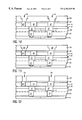
- FIG. 1 is a cross-sectional view of a multilevel interconnection pattern of prior art, depicting a plurality of metal spikes caused by the process of the prior art.
- FIG. 2 is a cross-sectional view of a substrate having a plurality of semiconductor devices, metallic via studs, which are substantially planar with the insulator layer, all formed by the process of the prior art.
- FIG. 3 shows the first step of the present invention for creating a self aligned barrier layer, where a thin layer of semiconductor passivation is etched out allowing for the via plug to protrude above the surface.
- FIG. 4 shows the next step of the process where a thin layer of barrier layer is deposited.
- FIG. 5 shows the self aligned barrier layer formed after polishing the structure of FIG. 4 .
- FIGS. 6, 7 and 8 show a sequence of process steps forming a level of high conductivity interconnection.
- FIGS. 9, 10 and 11 show sequential steps for forming via plugs and the next level of high conductivity interconnection lines using a double damascene method.
- FIGS. 12 and 13 illustrate another embodiment of this invention which uses the structure of FIG. 8, as the base to form the next level of high conductivity interconnection.
- FIG. 14 shows the first step of another embodiment of the present invention for creating a self aligned barrier layer, where a thin layer of semiconductor passivation is etched out allowing for the via plug to protrude above the surface.
- FIGS. 15, 16 and 17 illustrate the process of depositing a layer of barrier layer, planarizing the surface and making of blind holes.
- FIG. 18 illustrates the final structure made by another inventive process of this invention.
- the present interconnection technologies conventionally use tungsten or polysilicon to make contacts to devices. They also act as short local interconnect lines. These local interconnect lines are then joined to high conductivity interconnection lines, such as, for example, M 1 line, which is on a higher plane through via-plugs, such as, tungsten via-plugs.
- M 1 line high conductivity interconnection lines
- via-plugs such as, tungsten via-plugs.
- the local interconnects are normally separated from the M 1 line, usually by a layer of phospho-silicate glass (PSG).
- PSG phospho-silicate glass
- the via-interconnection between the first high conductivity metal lines (M 1 ) and the next level of high conductivity metal lines, such as, for example, M 2 line, is preferably made with the same high conductivity metal instead of tungsten.
- FIG. 1 A cross-section through a portion of a multi-level interconnection of the prior art is shown in FIG. 1 .
- devices or p/n junctions 12 are formed on a silicon substrate 10 .
- An insulator layer 20 is then formed over the substrate 10 , and using prior art methods interconnect or metallic stud 22 , are formed.
- Another insulator layer 30 is then formed over the insulator layer 20 .
- the insulator layer 30 is then etched and the openings are filled to form interconnect or metallic stud 32 .
- insulator layers 40 and 50 are formed and are subsequently etched to form interconnects 42 , 52 and 56 .
- etch-stop refers to a material or materials which are resistant to an etchant, when that etchant is used to remove-the insulator material above the etch-stop layer.
- silicon nitride is an etch-stop when etching a polyimide.
- An etch-stop layer such as a nitride layer can itself be removed by an etchant specific to it without removing polyimide.
- Interconnect 22 such as, short interconnects of tungsten 22 , make contacts to diffusion contacts 12 .
- a liner comprised of titanium and titanium-nitride is used as the diffusion contact.
- Interconnect 32 which basically comprises of tungsten via-plugs 32 , connects interconnects 22 , to high conductivity interconnection lines (M 1 ), such as, interconnect lines 42 .
- M 1 lines comprising of line 42 are connected to the M 2 lines comprising of line 56 , through via-plug or interconnect 52 .
- the via-plugs 52 could be tungsten, but, it is more desirable that the via-plugs 52 , are made of a high electrical conductivity metal. This is desirable for two reasons: firstly, to avoid the presence of dissimilar metal between high conductivity metals lines, such as, lines M 1 and M 2 , which may impede metal atom flow and that may cause electromigration failure; and secondly, for process cost saving, as the via-plug 52 , and the M 2 interconnection lines 56 , can be simultaneously formed by the dual damascene method.
- via-plugs metal lines or a combination of them, are typically formed by first depositing an insulator layer, such as, for example, a SiO 2 insulator layer. Patterns are then reactively ion etched to form via-holes, interconnection lines or a combination of via-hole and interconnection lines in this insulator layer. Liner materials can then be deposited and the rest of the holes or trenches can then be filled with metals. The excess metals from the field regions can be removed by chemical-mechanical polishing.
- an insulator layer such as, for example, a SiO 2 insulator layer.
- metal spikes 3 , 4 and 5 are formed when metal interconnections 52 , such as, via-studs 52 , does not fully land on the metal interconnection 42 , such as, lines 42 , due to a variety of reasons, such as, due to a misalignment.
- metal spikes 4 are formed when metal interconnection 42 , do not fully land on metal interconnect 32 , due to a variety of reasons, such as, due to a misalignment.
- metal spikes 3 are formed when via-studs 32 , do not fully land on metal interconnects 22 , due to a variety of reasons, such as, due to a misalignment.
- metal spikes 4 and 5 are the cause of:
- Another manifestation of the prior art process is the substantial reduction of the thickness of the high conductivity metal lines overlaying tungsten contact studs, as depicted in FIG. 1 .
- This thickness reduction substantially reduces electromigration life time of high conductivity metal interconnection lines.
- a simple and cost effective technique which comprises of unique sequences of process steps is provided which results in interconnection lines that are immune to misalignment, free of deleterious metal spikes, has minimum impact on cross-capacitance, and eliminates the defect with deleterious effect on electromigration.
- the invention is generally related to metal filled vias (via-plugs) and either filled or subtractively etched conductor lines on a substrate where the interconnection lines on different vertical levels are separated by a composite of two dielectric layers.
- the invention more particularly relates to improvements in sub-half-micron interconnections utilizing an improved double damascene method.
- the invention is not restricted to any particular metal or dielectric; also, the vias and conductor lines may comprise of same or different metals or layers of same or different metals.
- metal as referred here, may be a pure metal, an alloy, or may be comprised of layers of refractory and high electrical conductivity metals or alloys.
- FIG. 2 there is shown a cross-section of conventional semiconductor structure comprised of various device contacts and local interconnects or metallic studs 22 , typically tungsten with underlayers of titanium and titanium nitride (underlayers not shown), and metallic studs or via-plugs 32 .
- the local interconnects 22 , and the via-plugs 32 are formed by methods of the prior art, such as, for example, the damascene process.
- a pair of insulator layers 20 and 30 define the short interconnects and via studs pattern that are deposited on the surface of the substrate 10 .
- an insulator layer 20 is first deposited, planarized and then subsequently etched to form opening for metal interconnects.
- Metal interconnects 22 are then formed in the etched openings in the insulator layer 20 .
- an insulator layer 30 is then deposited and openings for the desired metal interconnects are etched.
- an overetching is done and when the interconnect metal is deposited in the etched opening in the insulator layer 30 , one gets interconnect 32 , with a spike 3 , in the overetching portion of the insulators 20 / 30 .
- the top surfaces of the via-plug 22 and 32 are substantially in plane with surface of surrounding insulator layers 20 and 30 , respectively.
- the insulator layers 20 and 30 are typically deposited SiO 2 layers.
- the spikes 3 that may be formed, are formed in the via-plugs 32 , and hence, have no deleterious effects of metal thinning as it would be in a metal conductor line; also there is no metal underneath to form a short.
- the next step is to form high conductivity metal interconnection.
- the substrate such as, shown in FIG. 2, is first processed to a point of being ready for the formation of first level of high conductivity interconnection metal lines.
- upper surface 31 , of the insulator layer 30 is lightly chemically-mechanically polished, or chemically etched to create protrusion 33 , from the metallic stud 32 . This could be done by removing, say about 50 nM of the top surface of the insulator layer 30 , without affecting the via plug 32 , such as, tungsten via plug 32 , or the insulator layer 20 .
- the insulator layer 20 has a different etch chemistry than the insulator layer 30 , which is above it, and which is self aligned with the via plug 32 .
- the next step is the deposition of a thin layer of an insulator 34 , e.g. MgO, Y 2 O 3 or Al 2 O 3 , as more clearly seen in FIG. 4 .
- This deposition of the insulator layer 34 can be done by any of the well known methods of the prior art, such as, for example, CVD, PECVD (Plasma Enhanced CVD), sputter deposition, to name a few.
- the insulator layer 34 is then lightly planarized, such as, by chemical-mechanical polishing, such that, the insulator layer 34 , over the tungsten plug 32 , is removed, so as to expose the surface of the via plug 32 , as more clearly seen in FIG. 5, where the insulator layer 34 , is self-aligned with the surface of the via plug 32 .
- the interconnection pattern of the 1st level of high conductivity metal is next defined by first depositing a layer of an insulation 40 , preferably, SiO 2 , over the exposed surfaces of the via plug 32 , and the insulator layer 34 , as clearly seen in FIG. 6, and then a layer of an insulator 44 .
- an insulation 40 preferably, SiO 2
- a first level of interconnection metal line pattern is defined by etching insulator layers 44 and 40 , to create opening or blind holes 45 .
- the metal line pattern is photolithographically defined and the insulators are reactively ion etched.
- the mutually exclusive etch characteristics of insulators 44 and 34 prevents etching of the other insulator layers, such as, insulator layers 34 or 30 , while insulator layers 44 or 40 , is being etched.
- the base of the etched blind hole 45 has not landed squarely on the upper surface of the via-plug 32 , but it is a little off-set and it does expose a portion of the surface 39 , of the insulator layer 34 , however, due to the mutually exclusive etch characteristics of insulators 34 and 40 , the etchant for layer 40 , will not etch or harm the exposed surface 39 , of the insulator layer 34 .
- etch barrier insulator layer 34 which is formed without the use of any mask, and which is also self-aligned with features underneath, prevents accidental etching of the insulator on the substrate, thereby preventing thinning of the first level of the high conductivity metal lines, thus, improving the electromigration life time.
- This insulator barrier layer 34 also plays another role, and that is that it also prevents accidental etching of the insulator 30 , on the substrate while the insulation 40 , above this first level of interconnection lines 32 , is being etched to form the next level of via plugs, thereby, preventing electrical short circuit between adjacent interconnection lines.
- the next step is to deposit at least one electrically conductive material 42 , into the blind hole 45 , so as to create metal interconnection 42 , and then the surface of this structure is planarized.
- conductive material 42 is a high conductivity metal 42 , such as, for example, aluminum, copper or alloys thereof.
- the formation of the conductive material 42 is preceded by the placement of a contact metal, for example, titanium or tantalum, and a barrier metal, for example, titanium nitride or tantalum-nitride, and optionally followed by CVD tungsten deposition.
- a contact metal for example, titanium or tantalum
- a barrier metal for example, titanium nitride or tantalum-nitride
- the next step is to form interlevel via-plugs and the next level of interconnection lines.
- this could be accomplished either by first forming a planarized set of via plugs and then forming the second level interconnection lines, or, by simultaneously forming the via plugs and the interconnection lines by a double damascene method.
- the double damascene method is a method of choice for better reliability and process ease, a double damascene process is described in U.S. Pat. No. 5,434,451 to Dalal et al. and assigned to the assignee of the present invention, and the disclosure of which is incorporated herein by reference.
- the next level of via-plugs and interconnection lines are achieved, by double damascene, by first depositing at least one layer of an insulator 50 , say SiO 2 . It is preferred that the thickness of the insulator layer 50 , is at least about 20 percent thicker than the combined desired length of the via-plug and thickness of metal interconnection lines.
- the design for via plugs and the second level of interconnection lines are preferably formed by photo-masking the area and then etching the insulator layer 50 , sequentially to create blind holes or openings 55 , for via plugs and interconnection lines pattern, as more clearly shown in FIG. 10 .
- the next step is to deposit at least one electrically conductive material 58 , into the blind hole 55 , so as to create metal interconnection 58 , and then the surface of this structure is planarized.
- conductive material 58 is a high conductivity metal 58 , such as, for example, aluminum, copper or alloys thereof.
- the formation of the conductive material 58 is preceded by the placement of a contact metal, for example, titanium or tantalum, and a barrier metal, for example, titanium nitride or tantalum-nitride, and optionally followed by CVD tungsten deposition.
- a contact metal for example, titanium or tantalum
- a barrier metal for example, titanium nitride or tantalum-nitride
- FIG. 11 also illustrates the final structure of one embodiment of this invention where the desired metals for the via plugs and interconnection lines 58 , have been deposited and the surface has been planarized to remove any excess materials.
- interlevel via-plugs are first defined and followed by definition of second level of interconnection lines. This embodiment is illustrated in FIGS. 8, and 12 through 18 .
- a layer of insulator 50 is deposited, and subsequently etched to form blind holes 56 , as per via-stud patterns, as shown in FIG. 12 .
- the next step is to deposit at least one electrically conductive material 52 , into the blind hole 56 , so as to create metal interconnection 52 , and then the surface of this structure is planarized.
- conductive material 52 is a high conductivity metal 52 , such as, for example, aluminum, copper or alloys thereof.
- the formation of the conductive material 52 is preceded by the placement of a contact metal, for example, titanium or tantalum, and a barrier metal, for example, titanium nitride or tantalum-nitride, and optionally followed by CVD tungsten deposition.
- a contact metal for example, titanium or tantalum
- a barrier metal for example, titanium nitride or tantalum-nitride
- the upper surface of the insulator layer 50 is lightly chemically-mechanically polished, or chemically etched to create protrusion 53 , from the metallic stud 52 . This could be done by removing, say about 50 nM of the top surface of the insulator layer 50 , without affecting the via plug 52 , such as, tungsten via plug 52 , or the insulator layer 44 .
- the insulator layer 44 has a different etch chemistry than the insulator layer 50 , which is above it, and which is self aligned with the via plug 52 .
- the next step is the deposition of a thin layer of an insulator 54 , e.g. MgO, Y 2 O 3 or Al 2 O 3 , as more clearly seen in FIG. 15 .
- This deposition of the insulator layer 54 can be done by any of the well known methods of the prior art, such as, for example, CVD, PECVD, sputter deposition, to name a few.
- the insulator layer 54 is then lightly planarized, such as, by chemical-mechanical polishing, such that, the insulator layer 54 , over the tungsten plug 52 , is removed, so as to expose the surface of the via plug 52 , as more clearly seen in FIG. 16, where the insulator layer 54 , is self-aligned with the surface of the via plug 52 .
- the second level of high conductivity metal interconnection lines are defined. This could be achieved by a damascene method, reactive ion etching of metal or simply chemical etching. Another advantage of this method is that the metals for the via plugs and the second level of interconnection metal lines could be different. This method is particularly of advantage where the first level of interconnection lines are defined by, say, aluminum-copper alloys and the desired metal for the second level of interconnection lines is, say, copper; then tungsten, aluminum-alloys or copper via plugs with optional cladding of titanium, titanium-nitride, tantalum, tantalum-nitride, chromium, tungsten or any combination of them, could be used.
- a layer of an insulation 60 preferably, SiO 2 , over the exposed surfaces of the via plug 52 , and the insulator layer 54 , is deposited, as clearly seen in FIG. 17 .
- a second level of interconnection metal line pattern is defined by etching insulator layer 60 , to create opening or blind hole 65 .
- This defining of the interconnection metal line pattern can be done by any of the methods which are well known in the art. However, the preferred method is photolithographically defining the metal line patterns.
- the mutually exclusive etch characteristics of insulators 54 and 60 prevents etching of the other insulator layers, such as, insulator layers 44 or 50 , while insulator layer 60 , is being etched.
- the etching of the blind hole 65 for the interconnection pattern, has not landing on upper surface of the via-plug 52 , but it is a little off-set and does expose a portion of the surface 59 , of the insulator layer 54 , however, due to the mutually exclusive etch characteristics of insulators 54 and 60 , the etchant for layer 60 , will not etch or harm the exposed surface 59 , of the insulator layer 54 .
- etch barrier insulator layer 54 which is formed without the use of any mask, and which is also self-aligned with features underneath, prevents accidental etching of the insulator on the substrate, thereby preventing thinning of the second level of the high conductivity metal lines, thus, improving the electromigration life time.
- This insulator barrier layer 54 also plays another role, and that is that it also prevents accidental etching of the insulator 50 , on the substrate while the insulation 60 , above the first level of interconnection lines 42 , is being etched, thereby, preventing electrical short circuit between adjacent interconnection lines.
- the next step is to deposit at least one electrically conductive material 62 , into the blind hole 65 , so as to create metal interconnection 62 , and then the surface of this structure is planarized.
- conductive material 62 is a high conductivity metal 62 , such as, for example, aluminum, copper or alloys thereof.
- the formation of the conductive material 62 is preceded by the placement of a contact metal, for example, titanium or tantalum, and a barrier metal, for example, titanium nitride or tantalum-nitride, and optionally followed by CVD tungsten deposition.
- a contact metal for example, titanium or tantalum
- a barrier metal for example, titanium nitride or tantalum-nitride
- the layer of insulation could be removed by a method selected from a group comprising reactive ion etching, wet chemical etching, chemical-mechanical polishing, to name a few.
- the first layer of insulation could be removed by a method selected from a group comprising reactive ion etching, sputter etching, ion beam etching, chemical-mechanical polishing, to name a few.
- the material for the first electrically conductive feature could be the same as the material for the subsequent electrically conductive feature, or it could be different.
- the electrically conductivity feature could comprise of layers of at least one contact metal, at least one barrier material, at least one high electrically conductive metal or alloy thereof.
- the contact metal could be selected from a group comprising tantalum, titanium, and alloys thereof.
- the barrier material could be selected from a group comprising chromium, chromium/chromium-oxide, cobalt, nickel, palladium, platinum, tantalum, tantalum-nitride, titanium-boride, titanium-nitride, titanium-oxy-nitride, titanium-silicide, titanium-tungsten, tungsten, tungsten-nitride, tungsten-silicon, and alloys thereof.
- the high electrically conductive metal could be selected from a group comprising aluminum, aluminum-copper, copper, copper-hafnium, copper-indium, copper-lanthanum, copper-tin, copper-zirconium, gold, silver, and alloys thereof, to name a few.
- the contact metal and/or the barrier material and/or the high conductivity metal could be deposited by a method selected from a group comprising sputtering, collimated sputtering, low pressure sputtering, reactive sputtering, electroplating, chemical vapor deposition, evaporation, to name a few.
- the material for the desired capping layer could be selected from a group comprising chromium, tantalum, tantalum nitride, titanium, titanium nitride, tungsten, tungsten nitride, tungsten-silicon, and alloys thereof, to name a few.
- the capping layer could be deposited by a method selected from a group comprising sputtering, collimated sputtering, low pressure sputtering, reactive sputtering, electroplating, chemical vapor deposition, evaporation, to name a few.
- the material for the different layers of insulation could be selected from a group comprising aluminum-oxide, magnesium-oxide, phospho-silicate glass, polyimide, silicon-nitride, silicon-oxide, yttrium-oxide, flowable oxide, diamond like dielectric, to name a few.
- Diamond like dielectric are materials that are single crystalline form of carbon, formed by methods, such as, high electrical discharge at high hydrostatic pressures or PECVD.
- Flowable oxides are materials that have very low dielectric constants and generally can be spun onto a part, such as, a wafer. Flowable oxide is a commercially available material and sold under various brand names, such as, for example, FOX, a Trademark of Dow Corning Corporation, Midland, Mich., USA.
- the insulator layers may be organic, in-organic or any combination of them and deposited by any, or several, of the known methods, such as, for example, CVD, PECVD, sputtering deposition, to name a few.
- the numbering, first and second level of high conductivity interconnection wiring is used for the purpose of illustration only and does not bound the use of the present invention to those numbered layers.
- the methods and the materials described for the first and the second level of interconnection wiring can be independently used for defining the circuitry at any desired level of interconnection.
Abstract
The present invention relates generally to a new sequence of methods and materials to improve the process yield and to enhance the reliability of multilevel interconnection with sub-half-micron geometry by making judicious use of composite insulators to prevent metal thinning over hard metal via plugs and by preventing process induced metal spike formation. The method takes advantage of the double damascene process. The metal spikes and the metal thinning resulting from over etch process is prevented in this method by using a pair of insulators which require different chemistries for etching.
Description
This patent application is a Div. of U.S. Ser. No. 08/947244, file Oct. 8, 1997, now U.S. Pat. No. 6,133,139.
This Patent Application is related to U.S. patent application Ser. No. 08/841,221, filed on Apr. 29, 1997, entitled, “SUB-HALF-MICRON MULTI-LEVEL INTERCONNECTION STRUCTURE AND PROCESS THEREOF”, U.S. patent application Ser. No. 08/840,432, filed on Apr. 29, 1997, entitled, “SUB-HALF-MICRON MULTI-LEVEL INTERCONNECTION STRUCTURE”, U.S. patent application Ser. No. 08/866,777, filed on May 30, 1997, entitled, “COPPER INTERCONNECTIONS WITH ENHANCED ELECTROMIGRATION RESISTANCE AND REDUCED DEFECT SENSITIVITY AND METHOD OF FORMING SAME”, and U.S. patent application Ser. No. 08/947,277 filed on Oct. 8, 1997, entitled, “SUB-QUARTER-MICRON COPPER INTERCONNECTIONS WITH IMPROVED ELECTROMIGRATION RESISTANCE AND REDUCED DEFECT SENSITIVITY”, all of which are presently assigned to the assignee of the instant application and the disclosure of which is incorporated herein by reference.
The present invention relates generally to a new semiconductor manufacturing, and more specifically to methods of forming interconnect structures in integrated circuits with improved circuit performance, reliability and process yield.
Current interconnection technologies conventionally use tungsten or polysilicon to make contacts to devices and also to act as a short local interconnect lines. These local interconnect lines are then joined to high conductivity interconnection lines (say M1) on a higher plane through tungsten via-plugs. The local interconnects are separated from the M1 layer usually by a layer of phospho-silicate glass (PSG).
The via-interconnection between the first high conductivity metal lines (M1) and the next level of high conductivity metal lines (say M2) is preferably made with the same high conductivity metal instead of tungsten.
Various other schemes for multilevel interconnection, and more particularly for utilization of a composite insulator, are taught in the prior art.
U.S. Pat. Nos. 3,837,907 (Berglund et al.) and 4,309,812 (Horng et al.) use a scheme, where composite insulators with different etching characteristics are used to make an overhung structure of insulator layers in order to reduce the spacing between the adjacent features. Berglund uses this scheme to reduce the spacing between the adjacent interconnect metal lines. However, this scheme is limited to metal lines running in any one particular direction which reduces its applicability.
U.S. Pat. No. 4,309,812 (Horng et al.), assigned to the instant assignee, and the disclosure of which is incorporated herein by reference, uses the above scheme to make closely spaced device contacts.
U.S. Pat. No. 5,326,426 (Tam et al.) utilize layers of different insulating material to provide a reflective coating for a laser mask.
U.S. Pat. No. 5,403,779 (Joshi et al.), assigned to the instant assignee, and the disclosure of which is incorporated herein by reference, teaches use of an organic dielectric layer sandwiched between inorganic dielectric layers.
It is well within the experience of artisans in this field that chemical/mechanical polishing of an organic layer produces debris thereby causing defects like metal opens and holes in the next level of dielectric.
U.S. Pat. No. 5,404,635 (Das) teaches use of a single dielectric layer to act as a spacer and an etch stop to fabricate thin film magnetic head.
U.S. Pat. No. 5,252,516 (Nguyen et al.), assigned to the assignee of the instant invention and the disclosure of which is incorporated herein by reference, teaches the use of a composite insulator comprised of a relatively thick layer of a reactively ion etchable dielectric and covered with a thin layer of an dielectric resistant to reactive etching.
U.S. Pat. No. 5,466,639 (Ireland), teaches double mask process for forming trenches and contacts during the formation of a semiconductor memory device. He shows another application of composite insulator to sequentially etch dielectric for the purpose of double damascene. Ireland uses a set of 3 dielectric layers to make cavity which consists of via stud and line patterns. However, the combination of three distinct layers of insulators causes charge trapment and dielectric losses.
U.S. Pat. No. 5,518,963 (Park), discloses a method for forming metal interconnection of semiconductor device. He uses insulating layer to etch a hole in one insulator while the second insulator protects the metal underneath from exposure to harsh etchants of the first insulator.
Artisans in the field of semiconductor integrated circuits are cognizant that multiple dielectric layers not only cause process complications and cost increase but more significantly it impedes the device functionality due to increased capacitance.
Thus, despite repeated efforts, and various schemes in the prior art, problems of leakage, short circuits, process yield, electromigration failure etc., remain and better methods, necessarily with simpler and fewer process steps, for making an integrated circuit pattern need to be developed.
The invention is a novel structure and a process for forming sub-half-micron multi-level high density electrical interconnect structures for integrated circuits.
Therefore, one purpose of this invention is to provide a structure and a process that will provide a means for fabricating an interconnection circuitry of sub-half-micron dimension with improved process yield, reliability and circuit performance.
Another purpose of this invention is to provide an interconnection process to prevent formation of undesired metal spikes.
Still another purpose of this invention is to prevent inter level short, or reliability exposing metal spike, caused by misalignment during a double damascene process.
Yet another purpose of this invention is to provide a thin insulating etch barrier over the insulator and which is self aligned with a via plug.
Still yet another purpose of the invention is to provide a minimum number of the etch barrier dielectric layers to reduce its effect on capacitance increase.
Therefore, in one aspect this invention comprises a method of forming multilevel interconnection lines and via-plugs of high conductivity metallurgy on top of a planarized substrate, said method comprising the steps of:
(a) on a substrate having at least one first electrically conductive feature surrounded by at least one layer of a first insulator, selectively removing a portion of said first insulator layer and exposing a portion of said first conductive feature,
(b) depositing at least one second layer of insulation over said exposed portion of said first conductive feature and said first insulator layer,
(c) selectively removing said second layer of insulation such that said exposed portion of said first conductive feature is again exposed and is substantially coplaner with said second layer of insulation,
(d) depositing at least one third layer of insulation over said first conductive feature and said second insulation layer,
(e) depositing at least one fourth layer of insulation over said third layer of insulation,
(f) forming at least one first blind hole in said third and said fourth layer of insulation such that at least a portion of the surface of said first electrically conductive feature is exposed,
(g) depositing at least one second electrically conductive feature in said at least one first blind hole, such that at least a portion of said second feature is in direct contact with at least a portion of said first feature,
(h) depositing at least one fifth layer of insulation over said second electrically conductive feature and said fourth insulation layer,
(i) forming at least one second blind hole in said fifth layer of insulation such that at least a portion of the surface of said second electrically conductive feature is exposed,
(j) depositing at least one third electrically conductive feature in said at least one second blind hole, such that at least a portion of said third feature is in direct contact with at least a portion of said second feature, and thereby forming said multilevel interconnection lines and via-plugs of high conductivity metallurgy on top of a planarized substrate.
In another aspect this invention comprises a method of forming multilevel interconnection lines and via-plugs of high conductivity metallurgy on top of a planarized substrate, said method comprising the steps of:
(a) on a substrate having at least one first electrically conductive feature surrounded by at least one layer of a first insulator, selectively removing a portion of said first insulator layer and exposing a portion of said first conductive feature,
(b) depositing at least one second layer of insulation over said exposed portion of said first conductive feature and said first insulator layer,
(c) selectively removing said second layer of insulation such that said exposed portion of said first conductive feature is again exposed and is substantially coplaner with said second layer of insulation,
(d) depositing at least one third layer of insulation over said first conductive feature and said second insulation layer,
(e) depositing at least one fourth layer of insulation over said third layer of insulation,
(f) forming at least one first blind hole in said third and said fourth layer of insulation such that at least a portion of the surface of said first electrically conductive feature is exposed,
(g) depositing at least one second electrically conductive feature in said at least one first blind hole, such that at least a portion of said second feature is in direct contact with at least a portion of said first feature,
(h) depositing at least one fifth layer of insulation over said second electrically conductive feature and said fourth insulation layer,
(i) forming at least one second blind hole in said fifth layer of insulation such that at least a portion of the surface of said second electrically conductive feature is exposed,
(j) depositing at least one third electrically conductive feature in said at least one second blind hole, such that at least a portion of said third feature is in direct contact with at least a portion of said second feature,
(k) selectively removing a portion of said fifth layer of insulation such that a portion of said third electrically conductive feature is exposed and protrudes above said fifth layer of insulation,
(l) depositing at least one sixth layer of insulation over said exposed portion of said third electrically conductive feature and said fifth insulator layer,
(m) selectively removing said sixth layer of insulation such that the surface of said third electrically conductive feature is exposed and is substantially coplaner with said sixth layer of insulation,
(n) depositing at least one seventh layer of insulation over said third electrically conductive feature and said sixth layer of insulation,
(o) forming at least one third blind hole in said seventh layer of insulation such that at least a portion of the surface of said third electrically conductive feature is exposed,
(p) depositing at least one fourth electrically conductive feature in said at least one third blind hole, such that at least a portion of said fourth feature is in direct contact with at least a portion of said third feature, and thereby forming said multilevel interconnection lines and via-plugs of high conductivity metallurgy on top of a planarized substrate.
In yet another aspect this invention comprises a method of forming interconnections between layers of a multilayer substrate comprising the steps of:
(a) providing a substrate including at least one first electrically conductive feature having a surface, said feature being surrounded by at least one layer of a first insulator,
(b) selectively removing a portion of said first insulator layer surrounding said first conductive feature and exposing a portion of said first conductive feature such that said surface of said first conductive feature is above the surrounding first insulator layer,
(c) depositing at least one etch stop insulator layer over said surface of said first conductive feature and said surrounding first insulator layer,
(d) selectively removing said etch stop insulator layer to expose said first electrically conductive feature and leaving at least a portion of said at least one first etch stop insulator layer surrounding said first electrically conductive feature,
(e) depositing at least one second insulator layer over said first electrically conductive feature and said portion of said etch stop insulator layer surrounding said first electrically conductive feature,
(f) etching said second insulator layer to form at least one blind hole in said second insulator layer such that at least a portion of said first electrically conductive feature and said portion of said etch-stop insulator layer surrounding said first electrically conductive feature is exposed,
(g) depositing at least one second electrically conductive feature in said at least one blind hole, such that at least a portion of said second conductive feature is in direct contact with at least a portion of said first conductive feature to form an interconnection between said first and second layers.
In yet another aspect this invention comprises a method of forming an etch barrier between layers of a multilayer substrate comprising the steps of:
(a) providing a substrate including at least one first electrically conductive feature having a surface, said feature being surrounded by at least one layer of a first insulator,
(b) selectively removing a portion of said first insulator layer surrounding said first conductive feature and exposing a portion of said first conductive feature such that said surface of said first conductive feature is above the surrounding first insulator layer,
(c) depositing at least one first etch stop insulator layer over said surface of said first conductive feature and said surrounding first insulator layer,
(d) selectively removing said etch stop insulator layer to expose said first electrically conductive feature and leaving at least a portion of said etch stop insulator layer surrounding said first electrically conductive feature, and thereby forming said etch barrier between layers of a multilayer substrate.
In still yet another aspect this invention comprises a semiconductor substrate having at least one high electrical conductivity interconnect, wherein said substrate comprising at least one p/n junction in electrical contact with a metallic via-plug, at least one first insulator layer over said semiconductor substrate and surrounding said first metallic via-plug, at least a portion of at least one first level of high electrical conductivity interconnection line in contact with said first metallic via-plug, wherein a second and a third insulator layer is over said first insulator layer and surrounds said first level electrical interconnection line, at least a portion of at least one second level electrical interconnection line in contact with said first level electrical interconnection line through at least one high electrical conductivity via-plug, wherein at least a fourth and a fifth insulator layer is over said third insulator layer and surrounds said second level electrical interconnection line, and wherein each adjoining insulator layer is of a different material, and thereby forming said semiconductor substrate having at least one high electrical conductivity interconnect.
The features of the invention believed to be novel and the elements characteristic of the invention are set forth with particularity in the appended claims. The drawings are for illustration purposes only and are not drawn to scale. Furthermore, like numbers represent like features in the drawings. The invention itself, however, both as to organization and method of operation, may best be understood by reference to the detailed description which follows taken in conjunction with the accompanying drawings in which:
FIG. 1, is a cross-sectional view of a multilevel interconnection pattern of prior art, depicting a plurality of metal spikes caused by the process of the prior art.
FIG. 2, is a cross-sectional view of a substrate having a plurality of semiconductor devices, metallic via studs, which are substantially planar with the insulator layer, all formed by the process of the prior art.
FIG. 3, shows the first step of the present invention for creating a self aligned barrier layer, where a thin layer of semiconductor passivation is etched out allowing for the via plug to protrude above the surface.
FIG. 4, shows the next step of the process where a thin layer of barrier layer is deposited.
FIG. 5, shows the self aligned barrier layer formed after polishing the structure of FIG. 4.
FIGS. 6, 7 and 8, show a sequence of process steps forming a level of high conductivity interconnection.
FIGS. 9, 10 and 11, show sequential steps for forming via plugs and the next level of high conductivity interconnection lines using a double damascene method.
FIGS. 12 and 13, illustrate another embodiment of this invention which uses the structure of FIG. 8, as the base to form the next level of high conductivity interconnection.
FIG. 14, shows the first step of another embodiment of the present invention for creating a self aligned barrier layer, where a thin layer of semiconductor passivation is etched out allowing for the via plug to protrude above the surface.
FIGS. 15, 16 and 17, illustrate the process of depositing a layer of barrier layer, planarizing the surface and making of blind holes.
FIG. 18, illustrates the final structure made by another inventive process of this invention.
The present interconnection technologies conventionally use tungsten or polysilicon to make contacts to devices. They also act as short local interconnect lines. These local interconnect lines are then joined to high conductivity interconnection lines, such as, for example, M1 line, which is on a higher plane through via-plugs, such as, tungsten via-plugs. The local interconnects are normally separated from the M1 line, usually by a layer of phospho-silicate glass (PSG).
The via-interconnection between the first high conductivity metal lines (M1) and the next level of high conductivity metal lines, such as, for example, M2 line, is preferably made with the same high conductivity metal instead of tungsten.
A cross-section through a portion of a multi-level interconnection of the prior art is shown in FIG. 1. On a silicon substrate 10, devices or p/n junctions 12, are formed. An insulator layer 20, is then formed over the substrate 10, and using prior art methods interconnect or metallic stud 22, are formed. Another insulator layer 30, is then formed over the insulator layer 20. The insulator layer 30, is then etched and the openings are filled to form interconnect or metallic stud 32. Similarly, insulator layers 40 and 50 are formed and are subsequently etched to form interconnects 42, 52 and 56.
As used herein, the term “etch-stop” refers to a material or materials which are resistant to an etchant, when that etchant is used to remove-the insulator material above the etch-stop layer. For example, silicon nitride is an etch-stop when etching a polyimide. An etch-stop layer such as a nitride layer can itself be removed by an etchant specific to it without removing polyimide.
Next, M1 lines comprising of line 42, are connected to the M2 lines comprising of line 56, through via-plug or interconnect 52. The via-plugs 52, could be tungsten, but, it is more desirable that the via-plugs 52, are made of a high electrical conductivity metal. This is desirable for two reasons: firstly, to avoid the presence of dissimilar metal between high conductivity metals lines, such as, lines M1 and M2, which may impede metal atom flow and that may cause electromigration failure; and secondly, for process cost saving, as the via-plug 52, and the M2 interconnection lines 56, can be simultaneously formed by the dual damascene method.
The method for dual damascene is taught by Dalal et al. in U.S. Pat. No. 5,434,451, assigned to the assignee of the present invention, and the disclosure of which is incorporated here by reference.
In the damascene method via-plugs, metal lines or a combination of them, are typically formed by first depositing an insulator layer, such as, for example, a SiO2 insulator layer. Patterns are then reactively ion etched to form via-holes, interconnection lines or a combination of via-hole and interconnection lines in this insulator layer. Liner materials can then be deposited and the rest of the holes or trenches can then be filled with metals. The excess metals from the field regions can be removed by chemical-mechanical polishing.
However, this prior art method has a problem of forming metal spikes, such as, metal spikes 3, 4 and 5. The metal spikes 5, are formed when metal interconnections 52, such as, via-studs 52, does not fully land on the metal interconnection 42, such as, lines 42, due to a variety of reasons, such as, due to a misalignment. Similarly, metal spikes 4, are formed when metal interconnection 42, do not fully land on metal interconnect 32, due to a variety of reasons, such as, due to a misalignment. And, similarly, metal spikes 3, are formed when via-studs 32, do not fully land on metal interconnects 22, due to a variety of reasons, such as, due to a misalignment.
Another reason for this spiking is that during etching of holes for via-studs an over-etch is generally practiced to ensure complete opening of holes across the wafer. This over-etching results in an undesired blind hole, which is normally formed, and which extends down towards the metal layer that is underneath, such as, the via-stud or interconnect layer. Consequently, metal spikes 3, 4 and 5, are formed when the grooves or over-etched blind holes are filled with the metal, as more clearly seen in FIG. 1.
These metal spikes, such as, metal spikes 4 and 5, are the cause of:
(a) time zero yield degradation due to electrical short between adjacent short channel metal wiring lines, especially around area 25, as shown in FIG. 1, if the metal spike 5, is deep or long enough to contact via-studs 32;
(b) exposure to reliability failure due to time dependent leakage generated by the higher electrical field at the tip of the metal spike; and,
(c) circuit performance degradation due to increased cross-capacitance between the adjacent lines caused by reduced spacing between the adjacent lines.
Another manifestation of the prior art process is the substantial reduction of the thickness of the high conductivity metal lines overlaying tungsten contact studs, as depicted in FIG. 1. This thickness reduction substantially reduces electromigration life time of high conductivity metal interconnection lines.
However, according to the present invention, a simple and cost effective technique which comprises of unique sequences of process steps is provided which results in interconnection lines that are immune to misalignment, free of deleterious metal spikes, has minimum impact on cross-capacitance, and eliminates the defect with deleterious effect on electromigration.
The invention is generally related to metal filled vias (via-plugs) and either filled or subtractively etched conductor lines on a substrate where the interconnection lines on different vertical levels are separated by a composite of two dielectric layers.
The invention more particularly relates to improvements in sub-half-micron interconnections utilizing an improved double damascene method. It should be understood that the invention is not restricted to any particular metal or dielectric; also, the vias and conductor lines may comprise of same or different metals or layers of same or different metals. Furthermore, it is well known to artisan in the field that metal, as referred here, may be a pure metal, an alloy, or may be comprised of layers of refractory and high electrical conductivity metals or alloys.
Referring to the drawings, wherein like reference numerals represent the same or similar parts throughout, and more particularly to FIG. 2, there is shown a cross-section of conventional semiconductor structure comprised of various device contacts and local interconnects or metallic studs 22, typically tungsten with underlayers of titanium and titanium nitride (underlayers not shown), and metallic studs or via-plugs 32. The local interconnects 22, and the via-plugs 32, are formed by methods of the prior art, such as, for example, the damascene process.
As shown in FIG. 2, a pair of insulator layers 20 and 30, define the short interconnects and via studs pattern that are deposited on the surface of the substrate 10. Basically, an insulator layer 20, is first deposited, planarized and then subsequently etched to form opening for metal interconnects. Metal interconnects 22, are then formed in the etched openings in the insulator layer 20. Subsequently, an insulator layer 30, is then deposited and openings for the desired metal interconnects are etched. In order to ensure electrical and mechanical contact, an overetching is done and when the interconnect metal is deposited in the etched opening in the insulator layer 30, one gets interconnect 32, with a spike 3, in the overetching portion of the insulators 20/30.
The excess materials from the metals 22 and 32, which are deposited in the insulator layer 20 and 30, are removed, such as, by Chemical-Mechanical polishing methods of the prior art.
It is preferred that the top surfaces of the via- plug 22 and 32, typically, tungsten, are substantially in plane with surface of surrounding insulator layers 20 and 30, respectively. The insulator layers 20 and 30, are typically deposited SiO2 layers. The spikes 3, that may be formed, are formed in the via-plugs 32, and hence, have no deleterious effects of metal thinning as it would be in a metal conductor line; also there is no metal underneath to form a short. The next step is to form high conductivity metal interconnection.
The substrate, such as, shown in FIG. 2, is first processed to a point of being ready for the formation of first level of high conductivity interconnection metal lines. As shown in FIG. 3, upper surface 31, of the insulator layer 30, is lightly chemically-mechanically polished, or chemically etched to create protrusion 33, from the metallic stud 32. This could be done by removing, say about 50 nM of the top surface of the insulator layer 30, without affecting the via plug 32, such as, tungsten via plug 32, or the insulator layer 20. Preferably the insulator layer 20, has a different etch chemistry than the insulator layer 30, which is above it, and which is self aligned with the via plug 32.
The next step is the deposition of a thin layer of an insulator 34, e.g. MgO, Y2O3 or Al2O3, as more clearly seen in FIG. 4. This deposition of the insulator layer 34, can be done by any of the well known methods of the prior art, such as, for example, CVD, PECVD (Plasma Enhanced CVD), sputter deposition, to name a few.
After the deposition, the insulator layer 34, is then lightly planarized, such as, by chemical-mechanical polishing, such that, the insulator layer 34, over the tungsten plug 32, is removed, so as to expose the surface of the via plug 32, as more clearly seen in FIG. 5, where the insulator layer 34, is self-aligned with the surface of the via plug 32.
The interconnection pattern of the 1st level of high conductivity metal is next defined by first depositing a layer of an insulation 40, preferably, SiO2, over the exposed surfaces of the via plug 32, and the insulator layer 34, as clearly seen in FIG. 6, and then a layer of an insulator 44.
As shown in FIG. 7, a first level of interconnection metal line pattern, is defined by etching insulator layers 44 and 40, to create opening or blind holes 45. Preferably the metal line pattern is photolithographically defined and the insulators are reactively ion etched.
The mutually exclusive etch characteristics of insulators 44 and 34, from that of the insulators 40 and 30, prevents etching of the other insulator layers, such as, insulator layers 34 or 30, while insulator layers 44 or 40, is being etched. As one can clearly see in FIG. 7, that the base of the etched blind hole 45, has not landed squarely on the upper surface of the via-plug 32, but it is a little off-set and it does expose a portion of the surface 39, of the insulator layer 34, however, due to the mutually exclusive etch characteristics of insulators 34 and 40, the etchant for layer 40, will not etch or harm the exposed surface 39, of the insulator layer 34.
Another advantage of the method of the present invention is that the etch barrier insulator layer 34, which is formed without the use of any mask, and which is also self-aligned with features underneath, prevents accidental etching of the insulator on the substrate, thereby preventing thinning of the first level of the high conductivity metal lines, thus, improving the electromigration life time.
This insulator barrier layer 34, also plays another role, and that is that it also prevents accidental etching of the insulator 30, on the substrate while the insulation 40, above this first level of interconnection lines 32, is being etched to form the next level of via plugs, thereby, preventing electrical short circuit between adjacent interconnection lines.
The next step, as shown in FIG. 8, is to deposit at least one electrically conductive material 42, into the blind hole 45, so as to create metal interconnection 42, and then the surface of this structure is planarized. It is preferred that conductive material 42, is a high conductivity metal 42, such as, for example, aluminum, copper or alloys thereof.
For some applications, it is also preferred that the formation of the conductive material 42, is preceded by the placement of a contact metal, for example, titanium or tantalum, and a barrier metal, for example, titanium nitride or tantalum-nitride, and optionally followed by CVD tungsten deposition.
As stated earlier excess material on the surface of this structure or outside the filled blind hole 45, are removed by methods well known in the prior art, such as, for example, chemical-mechanical polishing. This polishing or planarization can be done in a singular or in a sequence of multiple polishing steps, to leave the metal interconnection pattern 42, imbedded and substantially planar with the surface of the surrounding insulator 44, as clearly shown in FIG. 8.
The next step is to form interlevel via-plugs and the next level of interconnection lines. There are two ways this could be accomplished; either by first forming a planarized set of via plugs and then forming the second level interconnection lines, or, by simultaneously forming the via plugs and the interconnection lines by a double damascene method. The double damascene method is a method of choice for better reliability and process ease, a double damascene process is described in U.S. Pat. No. 5,434,451 to Dalal et al. and assigned to the assignee of the present invention, and the disclosure of which is incorporated herein by reference.
Referring now to FIG. 9, the next level of via-plugs and interconnection lines are achieved, by double damascene, by first depositing at least one layer of an insulator 50, say SiO2. It is preferred that the thickness of the insulator layer 50, is at least about 20 percent thicker than the combined desired length of the via-plug and thickness of metal interconnection lines.
The design for via plugs and the second level of interconnection lines are preferably formed by photo-masking the area and then etching the insulator layer 50, sequentially to create blind holes or openings 55, for via plugs and interconnection lines pattern, as more clearly shown in FIG. 10.
The next step, as shown in FIG. 11, is to deposit at least one electrically conductive material 58, into the blind hole 55, so as to create metal interconnection 58, and then the surface of this structure is planarized. It is preferred that conductive material 58, is a high conductivity metal 58, such as, for example, aluminum, copper or alloys thereof.
For some applications, it is also preferred that the formation of the conductive material 58, is preceded by the placement of a contact metal, for example, titanium or tantalum, and a barrier metal, for example, titanium nitride or tantalum-nitride, and optionally followed by CVD tungsten deposition.
As stated earlier excess material on the surface of this structure or outside the filled blind hole 55, are removed by methods well known in the prior art, such as, for example, chemical-mechanical polishing. This polishing or planarization can be done in a singular or in a sequence of multiple polishing steps, to leave the metal interconnection pattern 58, imbedded and substantially planar with the surface of the surrounding insulator 50, as clearly shown in FIG. 11.
FIG. 11, also illustrates the final structure of one embodiment of this invention where the desired metals for the via plugs and interconnection lines 58, have been deposited and the surface has been planarized to remove any excess materials.
It should be noted that the embodiment of the present invention, where the double damascene method is used, one gets simultaneous formation of via-plugs and the second level interconnection lines.
The formation of individual via plug layer and next interconnection line level is still the most common process of choice. In one embodiment of the present invention, interlevel via-plugs are first defined and followed by definition of second level of interconnection lines. This embodiment is illustrated in FIGS. 8, and 12 through 18.
On the structure of FIG. 8, a layer of insulator 50, is deposited, and subsequently etched to form blind holes 56, as per via-stud patterns, as shown in FIG. 12.
The next step, as shown in FIG. 13, is to deposit at least one electrically conductive material 52, into the blind hole 56, so as to create metal interconnection 52, and then the surface of this structure is planarized. It is preferred that conductive material 52, is a high conductivity metal 52, such as, for example, aluminum, copper or alloys thereof.
For some applications, it is also preferred that the formation of the conductive material 52, is preceded by the placement of a contact metal, for example, titanium or tantalum, and a barrier metal, for example, titanium nitride or tantalum-nitride, and optionally followed by CVD tungsten deposition.
As stated earlier excess material on the surface of this structure or outside the filled blind hole 56, are removed by methods well known in the prior art, such as, for example, chemical-mechanical polishing. This polishing or planarization can be done in a singular or in a sequence of multiple polishing steps, to leave the metal interconnection pattern 52, imbedded and substantially planar with the surface of the surrounding insulator 50, as clearly shown in FIG. 13.
As shown in FIG. 14, the upper surface of the insulator layer 50, is lightly chemically-mechanically polished, or chemically etched to create protrusion 53, from the metallic stud 52. This could be done by removing, say about 50 nM of the top surface of the insulator layer 50, without affecting the via plug 52, such as, tungsten via plug 52, or the insulator layer 44. Preferably the insulator layer 44, has a different etch chemistry than the insulator layer 50, which is above it, and which is self aligned with the via plug 52.
The next step is the deposition of a thin layer of an insulator 54, e.g. MgO, Y2O3 or Al2O3, as more clearly seen in FIG. 15. This deposition of the insulator layer 54, can be done by any of the well known methods of the prior art, such as, for example, CVD, PECVD, sputter deposition, to name a few.
After the deposition, the insulator layer 54, is then lightly planarized, such as, by chemical-mechanical polishing, such that, the insulator layer 54, over the tungsten plug 52, is removed, so as to expose the surface of the via plug 52, as more clearly seen in FIG. 16, where the insulator layer 54, is self-aligned with the surface of the via plug 52.
In the next set of process steps the second level of high conductivity metal interconnection lines are defined. This could be achieved by a damascene method, reactive ion etching of metal or simply chemical etching. Another advantage of this method is that the metals for the via plugs and the second level of interconnection metal lines could be different. This method is particularly of advantage where the first level of interconnection lines are defined by, say, aluminum-copper alloys and the desired metal for the second level of interconnection lines is, say, copper; then tungsten, aluminum-alloys or copper via plugs with optional cladding of titanium, titanium-nitride, tantalum, tantalum-nitride, chromium, tungsten or any combination of them, could be used.
In one embodiment of the present invention where a damascene method to define the second level of interconnection line pattern is used, a layer of an insulation 60, preferably, SiO2, over the exposed surfaces of the via plug 52, and the insulator layer 54, is deposited, as clearly seen in FIG. 17.
As shown in FIG. 17, a second level of interconnection metal line pattern, is defined by etching insulator layer 60, to create opening or blind hole 65. This defining of the interconnection metal line pattern can be done by any of the methods which are well known in the art. However, the preferred method is photolithographically defining the metal line patterns.
The mutually exclusive etch characteristics of insulators 54 and 60, prevents etching of the other insulator layers, such as, insulator layers 44 or 50, while insulator layer 60, is being etched. As one can clearly see in FIG. 17, that the etching of the blind hole 65, for the interconnection pattern, has not landing on upper surface of the via-plug 52, but it is a little off-set and does expose a portion of the surface 59, of the insulator layer 54, however, due to the mutually exclusive etch characteristics of insulators 54 and 60, the etchant for layer 60, will not etch or harm the exposed surface 59, of the insulator layer 54.
Another advantage of the method of the present invention is that the etch barrier insulator layer 54, which is formed without the use of any mask, and which is also self-aligned with features underneath, prevents accidental etching of the insulator on the substrate, thereby preventing thinning of the second level of the high conductivity metal lines, thus, improving the electromigration life time.
This insulator barrier layer 54, also plays another role, and that is that it also prevents accidental etching of the insulator 50, on the substrate while the insulation 60, above the first level of interconnection lines 42, is being etched, thereby, preventing electrical short circuit between adjacent interconnection lines.
The next step, as shown in FIG. 18, is to deposit at least one electrically conductive material 62, into the blind hole 65, so as to create metal interconnection 62, and then the surface of this structure is planarized. It is preferred that conductive material 62, is a high conductivity metal 62, such as, for example, aluminum, copper or alloys thereof.
For some applications, it is also preferred that the formation of the conductive material 62, is preceded by the placement of a contact metal, for example, titanium or tantalum, and a barrier metal, for example, titanium nitride or tantalum-nitride, and optionally followed by CVD tungsten deposition.
As stated earlier excess material on the surface of this structure or outside the filled blind hole 65, are removed by methods well known in the prior art, such as, for example, chemical-mechanical polishing. This polishing or planarization can be done in a singular or in a sequence of multiple polishing steps, to leave the metal interconnection pattern 62, imbedded and substantially planar with the surface of the surrounding insulator 60, as clearly shown in FIG. 18.
The layer of insulation could be removed by a method selected from a group comprising reactive ion etching, wet chemical etching, chemical-mechanical polishing, to name a few.
For some applications the first layer of insulation could be removed by a method selected from a group comprising reactive ion etching, sputter etching, ion beam etching, chemical-mechanical polishing, to name a few.
It should be understood that the material for the first electrically conductive feature could be the same as the material for the subsequent electrically conductive feature, or it could be different.
As stated earlier that the electrically conductivity feature could comprise of layers of at least one contact metal, at least one barrier material, at least one high electrically conductive metal or alloy thereof. However, the contact metal could be selected from a group comprising tantalum, titanium, and alloys thereof. While, the barrier material could be selected from a group comprising chromium, chromium/chromium-oxide, cobalt, nickel, palladium, platinum, tantalum, tantalum-nitride, titanium-boride, titanium-nitride, titanium-oxy-nitride, titanium-silicide, titanium-tungsten, tungsten, tungsten-nitride, tungsten-silicon, and alloys thereof. And, the high electrically conductive metal could be selected from a group comprising aluminum, aluminum-copper, copper, copper-hafnium, copper-indium, copper-lanthanum, copper-tin, copper-zirconium, gold, silver, and alloys thereof, to name a few.
For some applications the contact metal and/or the barrier material and/or the high conductivity metal, could be deposited by a method selected from a group comprising sputtering, collimated sputtering, low pressure sputtering, reactive sputtering, electroplating, chemical vapor deposition, evaporation, to name a few.
As stated earlier that one could form at least one capping layer over at least a portion of the electrically conductive feature, and wherein the material for the desired capping layer could be selected from a group comprising chromium, tantalum, tantalum nitride, titanium, titanium nitride, tungsten, tungsten nitride, tungsten-silicon, and alloys thereof, to name a few. And, the capping layer, could be deposited by a method selected from a group comprising sputtering, collimated sputtering, low pressure sputtering, reactive sputtering, electroplating, chemical vapor deposition, evaporation, to name a few.
The material for the different layers of insulation could be selected from a group comprising aluminum-oxide, magnesium-oxide, phospho-silicate glass, polyimide, silicon-nitride, silicon-oxide, yttrium-oxide, flowable oxide, diamond like dielectric, to name a few. Diamond like dielectric, are materials that are single crystalline form of carbon, formed by methods, such as, high electrical discharge at high hydrostatic pressures or PECVD. Flowable oxides are materials that have very low dielectric constants and generally can be spun onto a part, such as, a wafer. Flowable oxide is a commercially available material and sold under various brand names, such as, for example, FOX, a Trademark of Dow Corning Corporation, Midland, Mich., USA.
It should be apparent that given the guidance and the illustrations set forth herein, alternate embodiments of the processes and structures of the present invention may be suggested to a skilled artisan. For example, the insulator layers may be organic, in-organic or any combination of them and deposited by any, or several, of the known methods, such as, for example, CVD, PECVD, sputtering deposition, to name a few. The numbering, first and second level of high conductivity interconnection wiring, is used for the purpose of illustration only and does not bound the use of the present invention to those numbered layers. Likewise, the methods and the materials described for the first and the second level of interconnection wiring can be independently used for defining the circuitry at any desired level of interconnection.
While the present invention has been particularly described, in conjunction with a specific preferred embodiment, it is evident that many alternatives, modifications and variations will be apparent to those skilled in the art in light of the foregoing description. It is therefore contemplated that the appended claims will embrace any such alternatives, modifications and variations as falling within the true scope and spirit of the present invention.
Claims (12)
1. A semiconductor substrate having at least one high electrical conductivity interconnect, wherein said substrate comprising at least one p/n junction in electrical contact with a metallic via-plug, at least one first insulator layer over said semiconductor substrate and surrounding said first metallic via-plug, at least a portion of at least one first level of high electrical conductivity interconnection line in contact with said first metallic via-plug, wherein a second and a third insulator layers are over said first insulator layer and surrounds said first level electrical interconnection line, at least a portion of at least one second level electrical interconnection line in contact with said first level electrical interconnection line through at least one high electrical conductivity via-plug, wherein at least a fourth and a fifth insulator layers are over said third insulator layer and surrounds said second level electrical interconnection line, and wherein each adjoining insulator layer is of a different material, and thereby forming said semiconductor substrate having at least one high electrical conductivity interconnect.
2. The substrate of claim 1, wherein material for said first high electrical conductivity interconnection line is the same as material for said second high electrical conductivity interconnection line.
3. The substrate of claim 1, wherein material for said first high electrical conductivity interconnection line is different than the material for said second high electrical conductivity interconnection line.
4. The substrate of claim 1, wherein said first and/or second high electrical conductivity interconnection line comprises of at least one layer of a contact metal, a barrier metal and a high conductivity metal.
5. The substrate of claim 4, wherein said at least one contact metal is selected from a group consisting of tantalum, titanium or alloys thereof.
6. The substrate of claim 4, wherein said barrier material is selected from a group consisting of chromium, chromium/chromium-oxide, cobalt, nickel, palladium, platinum, tantalum, tantalum-nitride, titanium-boride, titanium-nitride, titanium-oxy-nitride, titanium-silicide, titanium-tungsten, tungsten, tungsten-nitride, tungsten-silicon and alloys thereof.
7. The substrate of claim 4, wherein at least one of said first and/or second high conductivity metal is selected from a group consisting of aluminum, aluminum-copper, copper, copper-hafnium, copper-indium, copper-lanthanum, copper-tin, copper-zirconium, gold, silver, and alloys thereof.
8. The substrate of claim 4, wherein said first and/or second high electrical conductivity interconnection has at least one cap layer, and wherein said cap layer is selected from a group consisting of chromium, tantalum, tantalum nitride, titanium, titanium nitride, tungsten, tungsten nitride, tungsten-silicon, and alloys thereof.
9. The substrate of claim 1, wherein said at least one metallic via-plug is substantially in coplanarity with said at least one insulator layer.
10. The substrate of claim 1, wherein material for said third and/or fifth insulator is selected from a group consisting of aluminum-oxide, magnesium-oxide, phospho-silicate glass, polyimide, silicon-nitride, silicon-oxide, yttrium-oxide, flowable oxide and diamond like dielectric.
11. The substrate of claim 1, wherein material for said second and/or fourth insulator layer is selected from a group consisting of aluminum-oxide, magnesium-oxide, phospho-silicate glass, polyimide, silicon-nitride, silicon-oxide and yttrium-oxide.
12. The substrate of claim 1, wherein material for said metallic via-plug is selected from a group consisting of aluminum, chromium, chromium/chromium-oxide, cobalt, copper, molybdenum, nickel, palladium, platinum, tantalum, tantalum-nitride, titanium, titanium-boride, titanium-nitride, titanium-oxy-nitride, titanium-silicide, titanium-tungsten, tungsten, tungsten-nitride, tungsten-silicon, and alloys thereof.
Priority Applications (1)
| Application Number | Priority Date | Filing Date | Title |
|---|---|---|---|
| US09/365,684 US6294835B1 (en) | 1997-10-08 | 1999-08-02 | Self-aligned composite insulator with sub-half-micron multilevel high density electrical interconnections and process thereof |
Applications Claiming Priority (2)
| Application Number | Priority Date | Filing Date | Title |
|---|---|---|---|
| US08/947,244 US6133139A (en) | 1997-10-08 | 1997-10-08 | Self-aligned composite insulator with sub-half-micron multilevel high density electrical interconnections and process thereof |
| US09/365,684 US6294835B1 (en) | 1997-10-08 | 1999-08-02 | Self-aligned composite insulator with sub-half-micron multilevel high density electrical interconnections and process thereof |
Related Parent Applications (1)
| Application Number | Title | Priority Date | Filing Date |
|---|---|---|---|
| US08/947,244 Division US6133139A (en) | 1997-10-08 | 1997-10-08 | Self-aligned composite insulator with sub-half-micron multilevel high density electrical interconnections and process thereof |
Publications (1)
| Publication Number | Publication Date |
|---|---|
| US6294835B1 true US6294835B1 (en) | 2001-09-25 |
Family
ID=25485812
Family Applications (2)
| Application Number | Title | Priority Date | Filing Date |
|---|---|---|---|
| US08/947,244 Expired - Fee Related US6133139A (en) | 1997-10-08 | 1997-10-08 | Self-aligned composite insulator with sub-half-micron multilevel high density electrical interconnections and process thereof |
| US09/365,684 Expired - Fee Related US6294835B1 (en) | 1997-10-08 | 1999-08-02 | Self-aligned composite insulator with sub-half-micron multilevel high density electrical interconnections and process thereof |
Family Applications Before (1)
| Application Number | Title | Priority Date | Filing Date |
|---|---|---|---|
| US08/947,244 Expired - Fee Related US6133139A (en) | 1997-10-08 | 1997-10-08 | Self-aligned composite insulator with sub-half-micron multilevel high density electrical interconnections and process thereof |
Country Status (1)
| Country | Link |
|---|---|
| US (2) | US6133139A (en) |
Cited By (15)
| Publication number | Priority date | Publication date | Assignee | Title |
|---|---|---|---|---|
| US6373688B1 (en) | 2001-07-12 | 2002-04-16 | General Electric Company | Service entrance barrier insulator |
| US6509593B2 (en) * | 2000-06-19 | 2003-01-21 | Fujitsu Limited | Semiconductor device and method of manufacturing the same |
| US6559047B1 (en) * | 2002-01-24 | 2003-05-06 | National Semiconductor Corporation | Method of forming a metal interconnect that substantially reduces the formation of intermetallic residue regions |
| US6657305B1 (en) * | 2000-11-01 | 2003-12-02 | International Business Machines Corporation | Semiconductor recessed mask interconnect technology |
| US6717266B1 (en) * | 2002-06-18 | 2004-04-06 | Advanced Micro Devices, Inc. | Use of an alloying element to form a stable oxide layer on the surface of metal features |
| US20040198036A1 (en) * | 2001-08-14 | 2004-10-07 | Makiko Nakamura | Semiconductor device having a tapered interconnection with insulating material on conductive sidewall thereof within through hole |
| US6825561B1 (en) | 2003-06-19 | 2004-11-30 | International Business Machines Corporation | Structure and method for eliminating time dependent dielectric breakdown failure of low-k material |
| US6858937B2 (en) * | 2000-03-02 | 2005-02-22 | Micron Technology, Inc. | Backend metallization method and device obtained therefrom |
| WO2008031255A1 (en) * | 2006-08-18 | 2008-03-20 | He Jian Technology(Suzhou)Co., Ltd | Method of self-aligned silicon nitride overlying for the borderless contact hole of copper technology |
| US20080217790A1 (en) * | 2007-03-09 | 2008-09-11 | Elpida Memory, Inc. | Semiconductor device and manufacturing method thereof |
| US20100025857A1 (en) * | 2008-07-29 | 2010-02-04 | Lindgren Peter J | Ic chip and design structure with through wafer vias dishing correction |
| US20100029075A1 (en) * | 2008-07-29 | 2010-02-04 | Lindgren Peter J | Through wafer vias with dishing correction methods |
| US20110233780A1 (en) * | 2007-04-09 | 2011-09-29 | Gordon Roy G | Cobalt nitride layers for copper interconnects and methods for forming them |
| CN102110624B (en) * | 2009-12-23 | 2012-05-30 | 中芯国际集成电路制造(上海)有限公司 | Method for detecting nickel and platinum removing device |
| US9466563B2 (en) * | 2014-12-01 | 2016-10-11 | Stmicroelectronics, Inc. | Interconnect structure for an integrated circuit and method of fabricating an interconnect structure |
Families Citing this family (19)
| Publication number | Priority date | Publication date | Assignee | Title |
|---|---|---|---|---|
| US5851916A (en) * | 1995-11-03 | 1998-12-22 | Micron Technology, Inc. | Formation of a self-aligned integrated circuit structures using planarization to form a top surface |
| JPH11220025A (en) * | 1998-02-03 | 1999-08-10 | Rohm Co Ltd | Semiconductor device and its manufacture |
| JPH11354637A (en) * | 1998-06-11 | 1999-12-24 | Oki Electric Ind Co Ltd | Connection structure for wiring and formation of connection part of the wiring |
| KR100267108B1 (en) * | 1998-09-16 | 2000-10-02 | 윤종용 | Semiconductor device having multi-layer metal interconnection and method fabricating the same |
| JP3436221B2 (en) | 1999-03-15 | 2003-08-11 | ソニー株式会社 | Manufacturing method of semiconductor device |
| US6900119B2 (en) | 2001-06-28 | 2005-05-31 | Micron Technology, Inc. | Agglomeration control using early transition metal alloys |
| US6770566B1 (en) | 2002-03-06 | 2004-08-03 | Cypress Semiconductor Corporation | Methods of forming semiconductor structures, and articles and devices formed thereby |
| US7119010B2 (en) * | 2002-04-23 | 2006-10-10 | Chartered Semiconductor Manfacturing Ltd. | Integrated circuit with self-aligned line and via and manufacturing method therefor |
| US6812576B1 (en) * | 2002-05-14 | 2004-11-02 | Applied Micro Circuits Corporation | Fanned out interconnect via structure for electronic package substrates |
| US6777318B2 (en) * | 2002-08-16 | 2004-08-17 | Taiwan Semiconductor Manufacturing Company | Aluminum/copper clad interconnect layer for VLSI applications |
| KR100560307B1 (en) * | 2002-12-30 | 2006-03-14 | 동부아남반도체 주식회사 | Fabricating method of semiconductor device |
| KR100539444B1 (en) * | 2003-07-11 | 2005-12-27 | 매그나칩 반도체 유한회사 | Method for forming a metal line in semiconductor device |
| JP3897006B2 (en) * | 2003-07-30 | 2007-03-22 | セイコーエプソン株式会社 | Method for forming multilayer wiring |
| US20110101534A1 (en) * | 2009-11-04 | 2011-05-05 | International Business Machines Corporation | Automated short length wire shape strapping and methods of fabricting the same |
| US20140299941A1 (en) * | 2013-04-04 | 2014-10-09 | Globalfoundries Inc. | Sram cell with reduced voltage droop |
| US9142488B2 (en) * | 2013-05-30 | 2015-09-22 | International Business Machines Corporation | Manganese oxide hard mask for etching dielectric materials |
| TWM521801U (en) * | 2015-05-29 | 2016-05-11 | Chunghwa Prec Test Tech Co Ltd | Adapting interface board with multi-layer structure with high bonding strength |
| US10366982B2 (en) | 2017-11-30 | 2019-07-30 | Taiwan Semiconductor Manufacturing Co., Ltd. | Structure with embedded memory device and contact isolation scheme |
| US11004794B2 (en) * | 2018-06-27 | 2021-05-11 | Taiwan Semiconductor Manufacturing Co., Ltd. | Partial barrier free vias for cobalt-based interconnects and methods of fabrication thereof |
Citations (23)
| Publication number | Priority date | Publication date | Assignee | Title |
|---|---|---|---|---|
| US3837907A (en) | 1972-03-22 | 1974-09-24 | Bell Telephone Labor Inc | Multiple-level metallization for integrated circuits |
| US4309812A (en) | 1980-03-03 | 1982-01-12 | International Business Machines Corporation | Process for fabricating improved bipolar transistor utilizing selective etching |
| US4622058A (en) | 1984-06-22 | 1986-11-11 | International Business Machines Corporation | Formation of a multi-layer glass-metallized structure formed on and interconnected to multi-layered-metallized ceramic substrate |
| US5252516A (en) | 1992-02-20 | 1993-10-12 | International Business Machines Corporation | Method for producing interlevel stud vias |
| US5284549A (en) | 1992-01-02 | 1994-02-08 | International Business Machines Corporation | Selective fluorocarbon-based RIE process utilizing a nitrogen additive |
| US5306947A (en) * | 1992-01-16 | 1994-04-26 | Mitsubishi Denki Kabushiki Kaisha | Semiconductor device and manufacturing method thereof |
| US5326526A (en) | 1990-10-18 | 1994-07-05 | Hitachi Powdered Metals Co., Ltd. | Sintered iron alloy composition and method of manufacturing the same |
| US5403779A (en) | 1992-02-26 | 1995-04-04 | International Business Machines Corporation | Refractory metal capped low resistivity metal conductor lines and vias formed using PVD and CVD |
| US5404638A (en) | 1991-02-15 | 1995-04-11 | Cardiac Pathways Corporation | Method of forming a flexible expandable member for use with a catheter probe |
| US5434451A (en) | 1993-01-19 | 1995-07-18 | International Business Machines Corporation | Tungsten liner process for simultaneous formation of integral contact studs and interconnect lines |
| US5466639A (en) | 1994-10-06 | 1995-11-14 | Micron Semiconductor, Inc. | Double mask process for forming trenches and contacts during the formation of a semiconductor memory device |
| US5518963A (en) | 1994-07-07 | 1996-05-21 | Hyundai Electronics Industries Co., Ltd. | Method for forming metal interconnection of semiconductor device |
| US5707901A (en) | 1994-06-29 | 1998-01-13 | Motorola, Inc. | Method utilizing an etch stop layer |
| US5736458A (en) | 1996-02-02 | 1998-04-07 | Taiwan Semiconductor Manufacturing Company, Ltd. | Method for improved aluminium-copper deposition and robust via contact resistance |
| US5792704A (en) | 1995-09-02 | 1998-08-11 | Lg Semicon Co., Ltd. | Method for fabricating wiring in semiconductor device |
| US5792705A (en) | 1996-06-28 | 1998-08-11 | Taiwan Semiconductor Manufacturing Company, Ltd. | Optimized planarization process for SOG filled vias |
| US5795820A (en) | 1996-07-01 | 1998-08-18 | Advanced Micro Devices | Method for simplifying the manufacture of an interlayer dielectric stack |
| US5801094A (en) | 1997-02-28 | 1998-09-01 | United Microelectronics Corporation | Dual damascene process |
| US5827776A (en) | 1996-07-18 | 1998-10-27 | Advanced Micro Devices, Inc. | Method of making an integrated circuit which uses an etch stop for producing staggered interconnect lines |
| US5840624A (en) | 1996-03-15 | 1998-11-24 | Taiwan Semiconductor Manufacturing Company, Ltd | Reduction of via over etching for borderless contacts |
| US5846876A (en) | 1996-06-05 | 1998-12-08 | Advanced Micro Devices, Inc. | Integrated circuit which uses a damascene process for producing staggered interconnect lines |
| US5856707A (en) * | 1995-09-11 | 1999-01-05 | Stmicroelectronics, Inc. | Vias and contact plugs with an aspect ratio lower than the aspect ratio of the structure in which they are formed |
| US5955781A (en) * | 1998-01-13 | 1999-09-21 | International Business Machines Corporation | Embedded thermal conductors for semiconductor chips |
Family Cites Families (2)
| Publication number | Priority date | Publication date | Assignee | Title |
|---|---|---|---|---|
| US5326426A (en) * | 1991-11-14 | 1994-07-05 | Tam Andrew C | Undercut membrane mask for high energy photon patterning |
| US5404635A (en) * | 1992-05-21 | 1995-04-11 | Das Devices, Inc. | Method of making a narrow track thin film head |
-
1997
- 1997-10-08 US US08/947,244 patent/US6133139A/en not_active Expired - Fee Related
-
1999
- 1999-08-02 US US09/365,684 patent/US6294835B1/en not_active Expired - Fee Related
Patent Citations (23)
| Publication number | Priority date | Publication date | Assignee | Title |
|---|---|---|---|---|
| US3837907A (en) | 1972-03-22 | 1974-09-24 | Bell Telephone Labor Inc | Multiple-level metallization for integrated circuits |
| US4309812A (en) | 1980-03-03 | 1982-01-12 | International Business Machines Corporation | Process for fabricating improved bipolar transistor utilizing selective etching |
| US4622058A (en) | 1984-06-22 | 1986-11-11 | International Business Machines Corporation | Formation of a multi-layer glass-metallized structure formed on and interconnected to multi-layered-metallized ceramic substrate |
| US5326526A (en) | 1990-10-18 | 1994-07-05 | Hitachi Powdered Metals Co., Ltd. | Sintered iron alloy composition and method of manufacturing the same |
| US5404638A (en) | 1991-02-15 | 1995-04-11 | Cardiac Pathways Corporation | Method of forming a flexible expandable member for use with a catheter probe |
| US5284549A (en) | 1992-01-02 | 1994-02-08 | International Business Machines Corporation | Selective fluorocarbon-based RIE process utilizing a nitrogen additive |
| US5306947A (en) * | 1992-01-16 | 1994-04-26 | Mitsubishi Denki Kabushiki Kaisha | Semiconductor device and manufacturing method thereof |
| US5252516A (en) | 1992-02-20 | 1993-10-12 | International Business Machines Corporation | Method for producing interlevel stud vias |
| US5403779A (en) | 1992-02-26 | 1995-04-04 | International Business Machines Corporation | Refractory metal capped low resistivity metal conductor lines and vias formed using PVD and CVD |
| US5434451A (en) | 1993-01-19 | 1995-07-18 | International Business Machines Corporation | Tungsten liner process for simultaneous formation of integral contact studs and interconnect lines |
| US5707901A (en) | 1994-06-29 | 1998-01-13 | Motorola, Inc. | Method utilizing an etch stop layer |
| US5518963A (en) | 1994-07-07 | 1996-05-21 | Hyundai Electronics Industries Co., Ltd. | Method for forming metal interconnection of semiconductor device |
| US5466639A (en) | 1994-10-06 | 1995-11-14 | Micron Semiconductor, Inc. | Double mask process for forming trenches and contacts during the formation of a semiconductor memory device |
| US5792704A (en) | 1995-09-02 | 1998-08-11 | Lg Semicon Co., Ltd. | Method for fabricating wiring in semiconductor device |
| US5856707A (en) * | 1995-09-11 | 1999-01-05 | Stmicroelectronics, Inc. | Vias and contact plugs with an aspect ratio lower than the aspect ratio of the structure in which they are formed |
| US5736458A (en) | 1996-02-02 | 1998-04-07 | Taiwan Semiconductor Manufacturing Company, Ltd. | Method for improved aluminium-copper deposition and robust via contact resistance |
| US5840624A (en) | 1996-03-15 | 1998-11-24 | Taiwan Semiconductor Manufacturing Company, Ltd | Reduction of via over etching for borderless contacts |
| US5846876A (en) | 1996-06-05 | 1998-12-08 | Advanced Micro Devices, Inc. | Integrated circuit which uses a damascene process for producing staggered interconnect lines |
| US5792705A (en) | 1996-06-28 | 1998-08-11 | Taiwan Semiconductor Manufacturing Company, Ltd. | Optimized planarization process for SOG filled vias |
| US5795820A (en) | 1996-07-01 | 1998-08-18 | Advanced Micro Devices | Method for simplifying the manufacture of an interlayer dielectric stack |
| US5827776A (en) | 1996-07-18 | 1998-10-27 | Advanced Micro Devices, Inc. | Method of making an integrated circuit which uses an etch stop for producing staggered interconnect lines |
| US5801094A (en) | 1997-02-28 | 1998-09-01 | United Microelectronics Corporation | Dual damascene process |
| US5955781A (en) * | 1998-01-13 | 1999-09-21 | International Business Machines Corporation | Embedded thermal conductors for semiconductor chips |
Cited By (25)
| Publication number | Priority date | Publication date | Assignee | Title |
|---|---|---|---|---|
| US6858937B2 (en) * | 2000-03-02 | 2005-02-22 | Micron Technology, Inc. | Backend metallization method and device obtained therefrom |
| US20060197231A1 (en) * | 2000-03-02 | 2006-09-07 | Chih-Chen Cho | Backend metallization method and device obtained therefrom |
| US7056823B2 (en) | 2000-03-02 | 2006-06-06 | Micron Technology, Inc. | Backend metallization method and device obtained therefrom |
| US20050116349A1 (en) * | 2000-03-02 | 2005-06-02 | Chih-Chen Cho | Backend metallization method and device obtained therefrom |
| US6509593B2 (en) * | 2000-06-19 | 2003-01-21 | Fujitsu Limited | Semiconductor device and method of manufacturing the same |
| US6657305B1 (en) * | 2000-11-01 | 2003-12-02 | International Business Machines Corporation | Semiconductor recessed mask interconnect technology |
| US20040051178A1 (en) * | 2000-11-01 | 2004-03-18 | International Business Machines Corporation | Semiconductor recessed mask interconnect technology |
| US6373688B1 (en) | 2001-07-12 | 2002-04-16 | General Electric Company | Service entrance barrier insulator |
| US20040198036A1 (en) * | 2001-08-14 | 2004-10-07 | Makiko Nakamura | Semiconductor device having a tapered interconnection with insulating material on conductive sidewall thereof within through hole |
| US6559047B1 (en) * | 2002-01-24 | 2003-05-06 | National Semiconductor Corporation | Method of forming a metal interconnect that substantially reduces the formation of intermetallic residue regions |
| US6717266B1 (en) * | 2002-06-18 | 2004-04-06 | Advanced Micro Devices, Inc. | Use of an alloying element to form a stable oxide layer on the surface of metal features |
| US20040256729A1 (en) * | 2003-06-19 | 2004-12-23 | International Business Machines Corporation | Structure and method for eliminating time dependent dielectric breakdown failure of low-k material |
| US6825561B1 (en) | 2003-06-19 | 2004-11-30 | International Business Machines Corporation | Structure and method for eliminating time dependent dielectric breakdown failure of low-k material |
| WO2008031255A1 (en) * | 2006-08-18 | 2008-03-20 | He Jian Technology(Suzhou)Co., Ltd | Method of self-aligned silicon nitride overlying for the borderless contact hole of copper technology |
| US20080217790A1 (en) * | 2007-03-09 | 2008-09-11 | Elpida Memory, Inc. | Semiconductor device and manufacturing method thereof |
| US8461684B2 (en) * | 2007-04-09 | 2013-06-11 | President And Fellows Of Harvard College | Cobalt nitride layers for copper interconnects and methods for forming them |
| US20110233780A1 (en) * | 2007-04-09 | 2011-09-29 | Gordon Roy G | Cobalt nitride layers for copper interconnects and methods for forming them |
| US7859114B2 (en) | 2008-07-29 | 2010-12-28 | International Business Machines Corporation | IC chip and design structure with through wafer vias dishing correction |
| US20100029075A1 (en) * | 2008-07-29 | 2010-02-04 | Lindgren Peter J | Through wafer vias with dishing correction methods |
| US8166651B2 (en) * | 2008-07-29 | 2012-05-01 | International Business Machines Corporation | Through wafer vias with dishing correction methods |
| US20120137515A1 (en) * | 2008-07-29 | 2012-06-07 | International Business Machines Corporation | Through wafer vias with dishing correction methods |
| US20100025857A1 (en) * | 2008-07-29 | 2010-02-04 | Lindgren Peter J | Ic chip and design structure with through wafer vias dishing correction |
| US8631570B2 (en) * | 2008-07-29 | 2014-01-21 | International Business Machines Corporation | Through wafer vias with dishing correction methods |
| CN102110624B (en) * | 2009-12-23 | 2012-05-30 | 中芯国际集成电路制造(上海)有限公司 | Method for detecting nickel and platinum removing device |
| US9466563B2 (en) * | 2014-12-01 | 2016-10-11 | Stmicroelectronics, Inc. | Interconnect structure for an integrated circuit and method of fabricating an interconnect structure |
Also Published As
| Publication number | Publication date |
|---|---|
| US6133139A (en) | 2000-10-17 |
Similar Documents
| Publication | Publication Date | Title |
|---|---|---|
| US6294835B1 (en) | Self-aligned composite insulator with sub-half-micron multilevel high density electrical interconnections and process thereof | |
| US5981374A (en) | Sub-half-micron multi-level interconnection structure and process thereof | |
| USRE37865E1 (en) | Semiconductor electrical interconnection methods | |
| US8951910B2 (en) | Methods for fabricating and forming semiconductor device structures including damascene structures | |
| US6239021B1 (en) | Dual barrier and conductor deposition in a dual damascene process for semiconductors | |
| US6245663B1 (en) | IC interconnect structures and methods for making same | |
| US4617193A (en) | Planar interconnect for integrated circuits | |
| US6800549B2 (en) | Method of fabricating semiconductor device including forming contact hole with anisotropic and isotropic etching and forming discontinuous barrier layer | |
| US7312532B2 (en) | Dual damascene interconnect structure with improved electro migration lifetimes | |
| KR100219508B1 (en) | Forming method for matal wiring layer of semiconductor device | |
| US5434451A (en) | Tungsten liner process for simultaneous formation of integral contact studs and interconnect lines | |
| KR100278662B1 (en) | Damascene metal wiring and forming method thereof | |
| US6372635B1 (en) | Method for making a slot via filled dual damascene low k interconnect structure without middle stop layer | |
| US5208170A (en) | Method for fabricating bipolar and CMOS devices in integrated circuits using contact metallization for local interconnect and via landing | |
| US6362526B1 (en) | Alloy barrier layers for semiconductors | |
| US6426558B1 (en) | Metallurgy for semiconductor devices | |
| US6939803B2 (en) | Method for forming conductor reservoir volume for integrated circuit interconnects | |
| US6350695B1 (en) | Pillar process for copper interconnect scheme | |
| US6232215B1 (en) | Method for forming increased density for interconnection metallization | |
| US6380625B2 (en) | Semiconductor interconnect barrier and manufacturing method thereof | |
| JP3415387B2 (en) | Semiconductor device and manufacturing method thereof | |
| US20020106885A1 (en) | Method of fabricating a slot dual damascene structure without middle stop layer | |
| US20020106895A1 (en) | Method for forming copper interconnect and enhancing electromigration resistance | |
| US20020127849A1 (en) | Method of manufacturing dual damascene structure | |
| US6365505B1 (en) | Method of making a slot via filled dual damascene structure with middle stop layer |
Legal Events
| Date | Code | Title | Description |
|---|---|---|---|
| FPAY | Fee payment |
Year of fee payment: 4 |
|
| REMI | Maintenance fee reminder mailed | ||
| LAPS | Lapse for failure to pay maintenance fees | ||
| STCH | Information on status: patent discontinuation |
Free format text: PATENT EXPIRED DUE TO NONPAYMENT OF MAINTENANCE FEES UNDER 37 CFR 1.362 |
|
| FP | Expired due to failure to pay maintenance fee |
Effective date: 20090925 |