US6236794B1 - Multi-section electro-optical monolithic component - Google Patents
Multi-section electro-optical monolithic component Download PDFInfo
- Publication number
- US6236794B1 US6236794B1 US09/327,533 US32753399A US6236794B1 US 6236794 B1 US6236794 B1 US 6236794B1 US 32753399 A US32753399 A US 32753399A US 6236794 B1 US6236794 B1 US 6236794B1
- Authority
- US
- United States
- Prior art keywords
- component
- sections
- waveguides
- waveguide
- width
- Prior art date
- Legal status (The legal status is an assumption and is not a legal conclusion. Google has not performed a legal analysis and makes no representation as to the accuracy of the status listed.)
- Expired - Lifetime
Links
Images



Classifications
-
- G—PHYSICS
- G02—OPTICS
- G02B—OPTICAL ELEMENTS, SYSTEMS OR APPARATUS
- G02B6/00—Light guides; Structural details of arrangements comprising light guides and other optical elements, e.g. couplings
- G02B6/10—Light guides; Structural details of arrangements comprising light guides and other optical elements, e.g. couplings of the optical waveguide type
- G02B6/12—Light guides; Structural details of arrangements comprising light guides and other optical elements, e.g. couplings of the optical waveguide type of the integrated circuit kind
- G02B6/12007—Light guides; Structural details of arrangements comprising light guides and other optical elements, e.g. couplings of the optical waveguide type of the integrated circuit kind forming wavelength selective elements, e.g. multiplexer, demultiplexer
-
- G—PHYSICS
- G02—OPTICS
- G02B—OPTICAL ELEMENTS, SYSTEMS OR APPARATUS
- G02B6/00—Light guides; Structural details of arrangements comprising light guides and other optical elements, e.g. couplings
- G02B6/10—Light guides; Structural details of arrangements comprising light guides and other optical elements, e.g. couplings of the optical waveguide type
- G02B6/12—Light guides; Structural details of arrangements comprising light guides and other optical elements, e.g. couplings of the optical waveguide type of the integrated circuit kind
- G02B6/12004—Combinations of two or more optical elements
-
- H—ELECTRICITY
- H01—ELECTRIC ELEMENTS
- H01S—DEVICES USING THE PROCESS OF LIGHT AMPLIFICATION BY STIMULATED EMISSION OF RADIATION [LASER] TO AMPLIFY OR GENERATE LIGHT; DEVICES USING STIMULATED EMISSION OF ELECTROMAGNETIC RADIATION IN WAVE RANGES OTHER THAN OPTICAL
- H01S5/00—Semiconductor lasers
- H01S5/02—Structural details or components not essential to laser action
- H01S5/026—Monolithically integrated components, e.g. waveguides, monitoring photo-detectors, drivers
- H01S5/0262—Photo-diodes, e.g. transceiver devices, bidirectional devices
-
- H—ELECTRICITY
- H01—ELECTRIC ELEMENTS
- H01S—DEVICES USING THE PROCESS OF LIGHT AMPLIFICATION BY STIMULATED EMISSION OF RADIATION [LASER] TO AMPLIFY OR GENERATE LIGHT; DEVICES USING STIMULATED EMISSION OF ELECTROMAGNETIC RADIATION IN WAVE RANGES OTHER THAN OPTICAL
- H01S5/00—Semiconductor lasers
- H01S5/02—Structural details or components not essential to laser action
- H01S5/026—Monolithically integrated components, e.g. waveguides, monitoring photo-detectors, drivers
- H01S5/0265—Intensity modulators
-
- H—ELECTRICITY
- H01—ELECTRIC ELEMENTS
- H01S—DEVICES USING THE PROCESS OF LIGHT AMPLIFICATION BY STIMULATED EMISSION OF RADIATION [LASER] TO AMPLIFY OR GENERATE LIGHT; DEVICES USING STIMULATED EMISSION OF ELECTROMAGNETIC RADIATION IN WAVE RANGES OTHER THAN OPTICAL
- H01S5/00—Semiconductor lasers
- H01S5/06—Arrangements for controlling the laser output parameters, e.g. by operating on the active medium
- H01S5/062—Arrangements for controlling the laser output parameters, e.g. by operating on the active medium by varying the potential of the electrodes
- H01S5/0625—Arrangements for controlling the laser output parameters, e.g. by operating on the active medium by varying the potential of the electrodes in multi-section lasers
-
- G—PHYSICS
- G02—OPTICS
- G02B—OPTICAL ELEMENTS, SYSTEMS OR APPARATUS
- G02B6/00—Light guides; Structural details of arrangements comprising light guides and other optical elements, e.g. couplings
- G02B6/10—Light guides; Structural details of arrangements comprising light guides and other optical elements, e.g. couplings of the optical waveguide type
- G02B6/12—Light guides; Structural details of arrangements comprising light guides and other optical elements, e.g. couplings of the optical waveguide type of the integrated circuit kind
- G02B2006/12083—Constructional arrangements
- G02B2006/12121—Laser
-
- G—PHYSICS
- G02—OPTICS
- G02B—OPTICAL ELEMENTS, SYSTEMS OR APPARATUS
- G02B6/00—Light guides; Structural details of arrangements comprising light guides and other optical elements, e.g. couplings
- G02B6/10—Light guides; Structural details of arrangements comprising light guides and other optical elements, e.g. couplings of the optical waveguide type
- G02B6/12—Light guides; Structural details of arrangements comprising light guides and other optical elements, e.g. couplings of the optical waveguide type of the integrated circuit kind
- G02B2006/12083—Constructional arrangements
- G02B2006/12123—Diode
-
- G—PHYSICS
- G02—OPTICS
- G02B—OPTICAL ELEMENTS, SYSTEMS OR APPARATUS
- G02B6/00—Light guides; Structural details of arrangements comprising light guides and other optical elements, e.g. couplings
- G02B6/10—Light guides; Structural details of arrangements comprising light guides and other optical elements, e.g. couplings of the optical waveguide type
- G02B6/12—Light guides; Structural details of arrangements comprising light guides and other optical elements, e.g. couplings of the optical waveguide type of the integrated circuit kind
- G02B2006/12133—Functions
- G02B2006/12142—Modulator
Definitions
- the present invention relates to a semiconductor electro-optical monolithic component made up of at least two sections disposed in line, each of which has a waveguide etched in the form of a ridge and buried in a cladding layer.
- FIG. 1 is a diagram in longitudinal section through an in-line transmitter-receiver device (1D-TRD) obtained by monolithically integrating a laser 30 and a detector 20 on the same substrate 10 .
- the laser 30 transmits a signal, e.g. at a wavelength of 1.3 ⁇ m to an optical fiber 50
- the detector receives a signal from the same optical fiber 50 , e.g. at a wavelength of 1.55 ⁇ m.
- the component since the transmit wavelength is shorter than the receive wavelength, the component includes a third section, disposed between the laser 30 and the detector 20 , and forming an optical isolator 40 .
- the purpose of the optical isolator 40 is to absorb the light emitted, at 1.3 ⁇ m, via the rear face of the laser, and thereby to prevent the detector from being dazzled, so that said detector can detect the optical signal at 1.55 ⁇ m coming from the optical fiber.
- the substrate 10 may, for example, be made of n-doped InP.
- the waveguides ( 21 , 31 ) respectively of the detector 20 , of the laser 30 , and of the optical isolator 40 are etched in the form of ridges and buried in a layer of highly-doped optical cladding 11 .
- the waveguides may be said to be of the “Buried Ridge Structure (BRS)” type.
- the cladding material is p+ doped when the substrate is n-doped. Since said material is highly doped, it is made conductive.
- FIG. 2A is a plan view of the component shown in FIG. 1, and FIG. 2B is a view in cross-section on A—A.
- conductive channels situated on either side of the waveguide 31 are referenced 12 .
- the presence of the conductive channels is due to the fact that the cladding layer 11 is highly doped.
- Proton implantation or lateral etching, referenced 15 in the diagram of FIG. 2B, and making the material resistive also enables the width of the conductive channels 12 to be limited to a value typically lying in the range 10 ⁇ m to 12 ⁇ m, and enables the component to be isolated laterally.
- the conductive channels 12 prevent very high resistance from being obtained at the interface between two sections.
- the waveguide 21 of the detector is, for example, made of a ternary material, while the waveguide 31 of the laser and of the optical isolator 40 is in the form of a quantum-well structure.
- metal electrodes 22 , 32 , 42 , 13 are formed on the various sections and on the bottom face of the component so as to enable it to operate.
- the first solution consists in growing, by epitaxy, a semi-insulating indium phosphide material (InP:Fe) at the interfaces between the sections.
- InP:Fe indium phosphide material
- the second solution consists in etching the cladding material 11 in the zones I situated at the interfaces between the sections.
- the third solution consists in implanting protons in the cladding material 11 locally in the zones I situated at the interfaces between the sections. In which case, the protons generate crystal defects which enable the population type to be reversed.
- the cladding material 11 is made locally semi-insulating, and therefore highly resistive.
- the optical losses, due to proton implantation at a density of 2 ⁇ 10 14 cm ⁇ 2 are about 0.8 dB for an implanted distance of length 5 ⁇ m, which corresponds to losses of about 3 dB for a component having two implanted sections of length 10 ⁇ m.
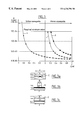
- curve a shown in FIG. 3 represents the value of the interface resistance R as a function of the distance h between the bottom of the implantation zone (or of the etching zone) I and the top surface of the waveguide, for a component shown in cross-section in FIG. 3 a and similar to the buried active ridge component shown in FIG. 1 .
- the curve shows that, in order to achieve resistance of not less than 15 k ⁇ , it is necessary to implant protons through the waveguide (or to etch through the waveguide), so that the bottom of the resistive zone I is situated at a distance h approximately in the range 0.8 ⁇ m to 0.9 ⁇ m below the top surfaces of the waveguides.
- Curve b in FIG. 3 shows the value of the interface resistance R as a function of the distance h between the bottom of the implantation zone (or of the etching zone) and the top surface of the waveguide for a prior art component in which the waveguide is of the ridge type, i.e. it is not etched.
- That component is shown in cross-section in FIG. 3 b, and it includes a top layer 14 which is deposited on the waveguide and which is etched over a width and a length that are determined to create a refractive index contrast, and to make it possible to guide light. In that component, the waveguides are not buried.
- Satisfactory resistance values R are obtained for implantation (or etching) depths in the top layer 14 that are sufficiently shallow, i.e. for depths such that the bottom of the resistive zone I is situated at a distance h lying in the range 0.2 ⁇ m to 0.1 ⁇ m above the top surface of the waveguide. Therefore, in that case, the waveguide is not degraded by the implantation (or the etching).
- An object of the present invention is to provide a multi-section electro-optical monolithic component having a buried active ridge (BRS type waveguide) and in which highly resistive electrical isolation zones I are formed at the interfaces between the sections over a depth that is shallow enough not to reach the waveguide.
- the component should also offer interface resistance values R of the same order of magnitude as those obtained with the ridge-type component.
- the invention provides a semiconductor electro-optical monolithic component made up of at least two sections, each of which has a respective waveguide, said waveguides being etched in the form of ridges, disposed in line, and buried in a cladding layer, and said sections being electrically isolated from one other by a resistive zone, wherein, at the interface between two sections, the waveguides are locally of an extended width not less than the width of the resistive zone.
- the waveguide ridges of the various sections of the component thus have locally extended zones making it possible to eliminate locally the conductive channels situated on either side of the waveguides, and therefore to increase the interface resistance.
- the resistive zone has a width not less than the conductive width of the cladding layer.
- the conductive width of the cladding layer is defined as being the sum of the widths of the conductive channels and of the waveguide buried in the cladding.
- Such a resistive zone width enables the conductive channels to be eliminated locally, and contributes to obtaining sufficient electrical isolation between two sections, i.e. resistance of not less than 15 k ⁇ .
- the resistive zone is obtained by locally implanting protons in the cladding layer, and it has a bottom situated at a distance not less than 0.08 ⁇ m above the top surfaces of the waveguides.
- the resistive zone is obtained by locally etching the cladding layer, and it has a bottom situated at a distance not less than 0.08 ⁇ m above the top surfaces of the waveguides.
- the resistance values obtained at the interfaces between the sections are very high. Typically, they may be not less than 15 k ⁇ . These values are obtained without the electrical isolation zone reaching the waveguide, so that optical losses at the interfaces between the sections are reduced considerably, and operation of the electro-optical component is not disturbed.
- FIG. 1 (described above) is a diagram in longitudinal section through a prior art in-line transmitter-receiver
- FIGS. 2A and 2B are respectively a plan view and a cross-section view of the component shown in FIG. 1;
- FIG. 3 shows curves a, b, and c indicating the value of the interface resistance R as a function of the distance h between the bottom of the resistive zone (I) and the top surfaces of the waveguides, the curves being associated respectively with respective ones of two prior art components shown in FIGS. 3 a and 3 b, and with a component of the invention shown in FIG. 3 c;
- FIGS. 4A and 4B are respective longitudinal section views of two types of in-line transmitter-receiver components of the invention.
- FIGS. 5A, 5 B, and 5 C are respectively a plan view of the component shown in FIG. 4, a view in cross-section through the electrical isolation zone of the FIG. 4 component, and a view in cross-section through one of the sections of the FIG. 4 component;
- FIGS. 6A and 6B are respectively a plan view and a cross-section view of a variant embodiment of the component shown in FIG. 4 A.
- FIGS. 4A and 4B show two types of in-line transmitter-receiver component of the invention, seen in longitudinal section.
- the component shown in FIG. 4A corresponds to the component shown in FIG. 1, and like references are used to designate like elements.
- the only visible difference compared with the prior art component as shown in FIG. 1 lies in the fact that the electrical isolation zones I are implemented over a depth that is shallow enough not to reach the waveguides 21 and 31 and to leave them intact.
- the component shown in FIG. 4B is made up of only two sections.
- the laser 30 transmits at a wavelength of 1.55 ⁇ m which is longer than the receive wavelength 1.3 ⁇ m of the detector 20 .
- the detector 20 therefore remains transparent at the wavelength 1.55 ⁇ m, and it correctly receives the signal that is sent to it at 1.3 ⁇ m, so that it is not necessary to place a light-absorbing section between the laser and the detector.
- the resistive zone I situated at the interface between the two sections is implemented in a manner such that it does not extend through the waveguides 21 , 31 .
- the in-line transmitter-receiver component shown in FIG. 4 A relate to the in-line transmitter-receiver component shown in FIG. 4 A.
- the invention is not limited to this type of component. It also applies to any multi-section electro-optical component including waveguide ridges buried in a cladding layer. For example, it is also applicable to multi-section lasers used to perform wavelength tuning, etc.
- FIGS. 5A, 5 B, and 5 C show the FIG. 4 component respectively in plan, and in cross-section.
- the width l I of the resistive zone I is defined along the width l of the component, and the length L I of the resistive zone I is defined along the length L of the component.
- the plan view of FIG. 5A shows that the waveguides 21 and 31 of the various sections, namely the detector 20 , the laser 30 , and the optical isolator 40 , are etched in the form of ridges, but that they are of larger width at the interfaces between the sections.
- the waveguide ridges 21 and 31 locally have respective widths 1 21 and 1 31 not less than the width l I of the resistive zone I.
- the waveguides are made locally wider at the interface between two sections over an overall length L 2 , L 3 preferably not less than the length L I of the resistive zone I.
- the overall length is defined as being the sum of the lengths of the wide portions of the various waveguides.
- the overall length L 2 of the wide zone corresponds to the length of the wide portion of the waveguide 31 added to the length of the wide portion of the other waveguide 21 .
- the view in cross-section on A—A of FIG. 5B shows the waveguide 31 at the interface between the laser section 30 and the optical isolator section 40 .
- the waveguide ridge 31 has an extended width l 31 equal to the width l I of the resistive zone I.
- the width of each of the conductive channels 12 is defined by a resistive zone 15 obtained previously by proton implantation or by etching so as to isolate the waveguide 31 laterally.
- the width of the resistive zone l I is thus preferably not less than the conductive width of the cladding layer 11 , i.e. not less than the sum of the widths of the waveguide 31 (l 31 ) and of the conductive channels 12 .
- the width l I of the resistive zone is thus defined by the lateral isolation zones 15 .
- the electrical isolation zone I is also formed over a depth p that is shallow enough not to extend through or even to reach the waveguide 31 .
- the resistive zone I has a bottom situated a certain distance h above the top surface of the waveguide 31 .
- the waveguide in a variant embodiment, and as shown diagrammatically in FIGS. 6A and 6B, it is possible for the waveguide to be locally non-etched below the isolation zone I so that it has a width l 31 , l 21 equal to the width l of the optical component.
- the electrical isolation zone I may be obtained independently by proton implantation or by etching the material of the cladding. Since the implantation or the etching does not extend through the waveguides, the optical losses at the interfaces between the sections of the in-line transmitter-receiver of the invention are reduced considerably.
- FIG. 3 shows three comparative curves of the value of the interface resistance R as a function of the distance h between the bottom of the resistive zone I and the top surface of the waveguide. Curves a and b are described above and they correspond to two prior art multi-section components.
- Level 0 of the distance h corresponds to the top surface of the waveguide.
- Curve c shows the interface resistance values R obtained with a component of the invention, shown in section in FIG. 3 c, and in which the waveguide ridges are buried in a cladding layer.
- the resistance values are close to those of the ridge-type prior art component.
- Interface resistance values R are obtained that are not less than 15 k ⁇ for distances h between the bottom of the resistance zone I and the top surface of the waveguide ridge that are not less than 0.08 ⁇ m.
- the difference between the curves b and c, corresponding respectively to the ridge-type prior art component and to the component of the invention, is simply due to the fact that in the ridge-type component, the resistive zone has a width l I of about 3 ⁇ m, whereas, the width l I of the isolation zone I of the component of the invention is slightly greater, e.g. about 10 ⁇ m.
- the invention is applicable not only to the above-described in-line transmitter-receiver. More generally, it is applicable to any multi-section monolithic electro-optical component having a buried active ridge. It is also independent of the composition and of the dimensions of the waveguides, and of the doping type (n or p) of the substrate and of the cladding layer.
Landscapes
- Physics & Mathematics (AREA)
- General Physics & Mathematics (AREA)
- Optics & Photonics (AREA)
- Condensed Matter Physics & Semiconductors (AREA)
- Electromagnetism (AREA)
- Engineering & Computer Science (AREA)
- Microelectronics & Electronic Packaging (AREA)
- Semiconductor Lasers (AREA)
- Optical Integrated Circuits (AREA)
- Light Receiving Elements (AREA)
Applications Claiming Priority (2)
| Application Number | Priority Date | Filing Date | Title |
|---|---|---|---|
| FR9807492 | 1998-06-15 | ||
| FR9807492A FR2779834B1 (fr) | 1998-06-15 | 1998-06-15 | Composant monolithique electro-optique multi-sections |
Publications (1)
| Publication Number | Publication Date |
|---|---|
| US6236794B1 true US6236794B1 (en) | 2001-05-22 |
Family
ID=9527374
Family Applications (1)
| Application Number | Title | Priority Date | Filing Date |
|---|---|---|---|
| US09/327,533 Expired - Lifetime US6236794B1 (en) | 1998-06-15 | 1999-06-08 | Multi-section electro-optical monolithic component |
Country Status (5)
| Country | Link |
|---|---|
| US (1) | US6236794B1 (de) |
| EP (1) | EP0966076A1 (de) |
| JP (1) | JP2000031581A (de) |
| CA (1) | CA2273427A1 (de) |
| FR (1) | FR2779834B1 (de) |
Cited By (2)
| Publication number | Priority date | Publication date | Assignee | Title |
|---|---|---|---|---|
| US6771682B2 (en) | 2002-08-12 | 2004-08-03 | Infinera Corporation | Electrical isolation of optical components in photonic integrated circuits (PICs) |
| US20060189016A1 (en) * | 2004-12-09 | 2006-08-24 | Park Moon H | Method of fabricating semiconductor optical device |
Citations (3)
| Publication number | Priority date | Publication date | Assignee | Title |
|---|---|---|---|---|
| JPS62291987A (ja) | 1986-06-12 | 1987-12-18 | Mitsubishi Electric Corp | 光集積化素子 |
| EP0314490A2 (de) | 1987-10-28 | 1989-05-03 | Kokusai Denshin Denwa Kabushiki Kaisha | Halbleiterlaser |
| EP0729042A1 (de) | 1995-02-22 | 1996-08-28 | Alcatel N.V. | Segmentierter optischer Leiter, dessen Verwendung insbesondere in einer Halbleitervorrichtung |
-
1998
- 1998-06-15 FR FR9807492A patent/FR2779834B1/fr not_active Expired - Fee Related
-
1999
- 1999-05-31 CA CA002273427A patent/CA2273427A1/fr not_active Abandoned
- 1999-06-08 US US09/327,533 patent/US6236794B1/en not_active Expired - Lifetime
- 1999-06-14 JP JP11167390A patent/JP2000031581A/ja active Pending
- 1999-06-14 EP EP99401447A patent/EP0966076A1/de not_active Withdrawn
Patent Citations (3)
| Publication number | Priority date | Publication date | Assignee | Title |
|---|---|---|---|---|
| JPS62291987A (ja) | 1986-06-12 | 1987-12-18 | Mitsubishi Electric Corp | 光集積化素子 |
| EP0314490A2 (de) | 1987-10-28 | 1989-05-03 | Kokusai Denshin Denwa Kabushiki Kaisha | Halbleiterlaser |
| EP0729042A1 (de) | 1995-02-22 | 1996-08-28 | Alcatel N.V. | Segmentierter optischer Leiter, dessen Verwendung insbesondere in einer Halbleitervorrichtung |
Non-Patent Citations (2)
| Title |
|---|
| Lammert R. M. et al.: "InGaAS-GaAs Quantum-Well Lasers with Monolithically Integrated Intracavity Electroabsorption Modulators by Selective-Area MOCVD" IEEE Photonics Technology Letters, vol. 8, No. 1, Jan. 1, 1996, pp. 78-80, XP000547540. |
| Ramdane A. Et al.: "Very Simple Approach for High Performance DFB Laser-Electroabsorption Modulator Monolithic Integration" Electronic Letters, vol. 30, No. 23, Nov. 10, 1994, p. 1980-1981 XP000495748. |
Cited By (5)
| Publication number | Priority date | Publication date | Assignee | Title |
|---|---|---|---|---|
| US6771682B2 (en) | 2002-08-12 | 2004-08-03 | Infinera Corporation | Electrical isolation of optical components in photonic integrated circuits (PICs) |
| US20040218850A1 (en) * | 2002-08-12 | 2004-11-04 | Infinera Corporation | Electrical isolation of optical components in photonic integrated circuits (PICs) |
| US6999489B2 (en) | 2002-08-12 | 2006-02-14 | Infinera Corporation | Electrical isolation of optical components in photonic integrated circuits (PICs) |
| US20060189016A1 (en) * | 2004-12-09 | 2006-08-24 | Park Moon H | Method of fabricating semiconductor optical device |
| US7378292B2 (en) | 2004-12-09 | 2008-05-27 | Electronics And Telecommunications Research Institute | Method of fabricating semiconductor optical device |
Also Published As
| Publication number | Publication date |
|---|---|
| FR2779834B1 (fr) | 2000-08-04 |
| EP0966076A1 (de) | 1999-12-22 |
| CA2273427A1 (fr) | 1999-12-15 |
| JP2000031581A (ja) | 2000-01-28 |
| FR2779834A1 (fr) | 1999-12-17 |
Similar Documents
| Publication | Publication Date | Title |
|---|---|---|
| US5416866A (en) | Optical waveguide/grating device for filtering optical wavelengths | |
| US5953479A (en) | Tilted valance-band quantum well double heterostructures for single step active and passive optical waveguide device monolithic integration | |
| US5737474A (en) | Semiconductor optical device | |
| JP3285426B2 (ja) | 半導体光集積素子及びその製造方法 | |
| US5457569A (en) | Semiconductor amplifier or laser having integrated lens | |
| US7199441B2 (en) | Optical module device driven by a single power supply | |
| EP0602873A1 (de) | Optische Vielfachschalteranordnung unter Verwendung halbleitender Wellenleiterverstärker | |
| US7127145B2 (en) | Semiconductor optical amplifier, and optical module using the same | |
| JPH0636457B2 (ja) | 半導体レ−ザを組み込むモノリシツク集積光学デバイスの製造方法およびこの方法によつて得られたデバイス | |
| US4847844A (en) | Surface-emitting semiconductor laser device | |
| JP2870632B2 (ja) | 半導体光集積回路およびその製造方法 | |
| US5796768A (en) | Buried structure laser device for integrated photonic circuit and method of manufacture | |
| EP0746784B1 (de) | Hochleistungs-wellenleitermodulator vom absorptionstyp | |
| CA2165711C (en) | Semiconductor light source having a spectrally broad, high power optical output | |
| US5301202A (en) | Semiconductor ridge waveguide laser with asymmetrical cladding | |
| US5454058A (en) | Selective optical signal switch and/or combiner | |
| CN113169516A (zh) | 一种具有更大动态范围的光放大器 | |
| EP0285104A2 (de) | Halbleiterlaser mit verteilter Rückkopplung | |
| EP0197084B1 (de) | Injektionslaserstruktur mit niedrigem rauschen | |
| US6411763B1 (en) | Integrated optical component | |
| US6236794B1 (en) | Multi-section electro-optical monolithic component | |
| US6137625A (en) | Semiconductor optical amplifier and integrated laser source information | |
| US6608850B1 (en) | Semiconductor laser apparatus | |
| CN114128061A (zh) | 一种波导结构、集成光芯片及实现电学隔离的方法 | |
| US5424242A (en) | Method for making an optoelectronic amplifier device, and applications to various optoelectronic |
Legal Events
| Date | Code | Title | Description |
|---|---|---|---|
| AS | Assignment |
Owner name: ALCATEL, FRANCE Free format text: ASSIGNMENT OF ASSIGNORS INTEREST;ASSIGNORS:MALLECOT, FRANCK;PLAIS, ANTONINA;CHAUMONT, CHRISTINE;REEL/FRAME:010025/0356 Effective date: 19990506 |
|
| STCF | Information on status: patent grant |
Free format text: PATENTED CASE |
|
| FEPP | Fee payment procedure |
Free format text: PAYOR NUMBER ASSIGNED (ORIGINAL EVENT CODE: ASPN); ENTITY STATUS OF PATENT OWNER: LARGE ENTITY |
|
| AS | Assignment |
Owner name: AVANEX CORPORATION, CALIFORNIA Free format text: ASSIGNMENT OF ASSIGNORS INTEREST;ASSIGNOR:ALCATEL;REEL/FRAME:014074/0489 Effective date: 20030731 |
|
| FPAY | Fee payment |
Year of fee payment: 4 |
|
| AS | Assignment |
Owner name: HBK INVESTMENTS L.P., TEXAS Free format text: SECURITY AGREEMENT;ASSIGNOR:AVANEX CORPORATION;REEL/FRAME:016079/0174 Effective date: 20050519 |
|
| AS | Assignment |
Owner name: AVANEX CORPORATION, CALIFORNIA Free format text: RELEASE BY SECURED PARTY;ASSIGNOR:HBK INVESTMENTS, L.P.;REEL/FRAME:019035/0342 Effective date: 20070312 |
|
| FPAY | Fee payment |
Year of fee payment: 8 |
|
| AS | Assignment |
Owner name: WELLS FARGO CAPITAL FINANCE, INC., AS AGENT, CALIF Free format text: PATENT SECURITY AGREEMENT;ASSIGNOR:OCLARO (NORTH AMERICA), INC.;REEL/FRAME:028487/0112 Effective date: 20110726 |
|
| FPAY | Fee payment |
Year of fee payment: 12 |
|
| AS | Assignment |
Owner name: SILICON VALLEY BANK, CALIFORNIA Free format text: SECURITY INTEREST;ASSIGNORS:OCLARO, INC.;OCLARO TECHNOLOGY, INC.;OCLARO (NORTH AMERICA), INC.;AND OTHERS;REEL/FRAME:032589/0948 Effective date: 20140328 |
|
| AS | Assignment |
Owner name: OCLARO (NORTH AMERICA), INC., CALIFORNIA Free format text: RELEASE BY SECURED PARTY;ASSIGNOR:WELLS FARGO CAPITAL FINANCE, LLC;REEL/FRAME:032643/0427 Effective date: 20140325 |
|
| AS | Assignment |
Owner name: OCLARO (NORTH AMERICA), INC., CALIFORNIA Free format text: CHANGE OF NAME;ASSIGNOR:AVANEX CORPORATION;REEL/FRAME:032826/0276 Effective date: 20090707 |
|
| AS | Assignment |
Owner name: OCLARO TECHNOLOGY LIMITED, CALIFORNIA Free format text: RELEASE BY SECURED PARTY;ASSIGNOR:SILICON VALLEY BANK;REEL/FRAME:042430/0235 Effective date: 20170331 Owner name: BOOKHAM NOMINEES LIMITED, CALIFORNIA Free format text: RELEASE BY SECURED PARTY;ASSIGNOR:SILICON VALLEY BANK;REEL/FRAME:042430/0235 Effective date: 20170331 Owner name: OCLARO (NORTH AMERICA), INC., CALIFORNIA Free format text: RELEASE BY SECURED PARTY;ASSIGNOR:SILICON VALLEY BANK;REEL/FRAME:042430/0235 Effective date: 20170331 Owner name: OCLARO INNOVATIONS LLP, CALIFORNIA Free format text: RELEASE BY SECURED PARTY;ASSIGNOR:SILICON VALLEY BANK;REEL/FRAME:042430/0235 Effective date: 20170331 Owner name: OCLARO TECHNOLOGY, INC., CALIFORNIA Free format text: RELEASE BY SECURED PARTY;ASSIGNOR:SILICON VALLEY BANK;REEL/FRAME:042430/0235 Effective date: 20170331 Owner name: MINTERA CORPORATION, CALIFORNIA Free format text: RELEASE BY SECURED PARTY;ASSIGNOR:SILICON VALLEY BANK;REEL/FRAME:042430/0235 Effective date: 20170331 Owner name: OPNEXT SUBSYSTEMS INC., CALIFORNIA Free format text: RELEASE BY SECURED PARTY;ASSIGNOR:SILICON VALLEY BANK;REEL/FRAME:042430/0235 Effective date: 20170331 Owner name: PINE PHOTONICS COMMUNICATIONS, INC., CALIFORNIA Free format text: RELEASE BY SECURED PARTY;ASSIGNOR:SILICON VALLEY BANK;REEL/FRAME:042430/0235 Effective date: 20170331 Owner name: OCLARO, INC., CALIFORNIA Free format text: RELEASE BY SECURED PARTY;ASSIGNOR:SILICON VALLEY BANK;REEL/FRAME:042430/0235 Effective date: 20170331 Owner name: OPNEXT, INC., CALIFORNIA Free format text: RELEASE BY SECURED PARTY;ASSIGNOR:SILICON VALLEY BANK;REEL/FRAME:042430/0235 Effective date: 20170331 |
|
| AS | Assignment |
Owner name: LUMENTUM OPTICS INC., CALIFORNIA Free format text: CHANGE OF NAME;ASSIGNOR:OCLARO, INC.;REEL/FRAME:049783/0733 Effective date: 20190603 |