EP0966076A1 - Aus mehreren Abschnitten bestehendes elektrooptisches monolithisches Bauelement - Google Patents
Aus mehreren Abschnitten bestehendes elektrooptisches monolithisches Bauelement Download PDFInfo
- Publication number
- EP0966076A1 EP0966076A1 EP99401447A EP99401447A EP0966076A1 EP 0966076 A1 EP0966076 A1 EP 0966076A1 EP 99401447 A EP99401447 A EP 99401447A EP 99401447 A EP99401447 A EP 99401447A EP 0966076 A1 EP0966076 A1 EP 0966076A1
- Authority
- EP
- European Patent Office
- Prior art keywords
- sections
- component
- width
- waveguide
- resistive zone
- Prior art date
- Legal status (The legal status is an assumption and is not a legal conclusion. Google has not performed a legal analysis and makes no representation as to the accuracy of the status listed.)
- Withdrawn
Links
- 239000004065 semiconductor Substances 0.000 claims abstract description 4
- 238000002513 implantation Methods 0.000 claims description 12
- 238000005530 etching Methods 0.000 claims description 7
- 230000003287 optical effect Effects 0.000 description 15
- 239000000463 material Substances 0.000 description 10
- 238000010292 electrical insulation Methods 0.000 description 8
- 239000012212 insulator Substances 0.000 description 6
- 238000002955 isolation Methods 0.000 description 5
- 238000009413 insulation Methods 0.000 description 4
- 239000000758 substrate Substances 0.000 description 4
- GPXJNWSHGFTCBW-UHFFFAOYSA-N Indium phosphide Chemical compound [In]#P GPXJNWSHGFTCBW-UHFFFAOYSA-N 0.000 description 3
- 239000004020 conductor Substances 0.000 description 3
- 239000013078 crystal Substances 0.000 description 3
- 230000007547 defect Effects 0.000 description 3
- 238000010586 diagram Methods 0.000 description 3
- 239000013307 optical fiber Substances 0.000 description 3
- 239000000203 mixture Substances 0.000 description 2
- 230000002745 absorbent Effects 0.000 description 1
- 239000002250 absorbent Substances 0.000 description 1
- 238000000149 argon plasma sintering Methods 0.000 description 1
- 238000005253 cladding Methods 0.000 description 1
- 230000000052 comparative effect Effects 0.000 description 1
- 238000000407 epitaxy Methods 0.000 description 1
- 239000000835 fiber Substances 0.000 description 1
- 230000004313 glare Effects 0.000 description 1
- 239000007943 implant Substances 0.000 description 1
- 238000009776 industrial production Methods 0.000 description 1
- 230000010354 integration Effects 0.000 description 1
- 230000003993 interaction Effects 0.000 description 1
- 229910052751 metal Inorganic materials 0.000 description 1
- 239000002184 metal Substances 0.000 description 1
Images


Classifications
-
- G—PHYSICS
- G02—OPTICS
- G02B—OPTICAL ELEMENTS, SYSTEMS OR APPARATUS
- G02B6/00—Light guides; Structural details of arrangements comprising light guides and other optical elements, e.g. couplings
- G02B6/10—Light guides; Structural details of arrangements comprising light guides and other optical elements, e.g. couplings of the optical waveguide type
- G02B6/12—Light guides; Structural details of arrangements comprising light guides and other optical elements, e.g. couplings of the optical waveguide type of the integrated circuit kind
- G02B6/12007—Light guides; Structural details of arrangements comprising light guides and other optical elements, e.g. couplings of the optical waveguide type of the integrated circuit kind forming wavelength selective elements, e.g. multiplexer, demultiplexer
-
- G—PHYSICS
- G02—OPTICS
- G02B—OPTICAL ELEMENTS, SYSTEMS OR APPARATUS
- G02B6/00—Light guides; Structural details of arrangements comprising light guides and other optical elements, e.g. couplings
- G02B6/10—Light guides; Structural details of arrangements comprising light guides and other optical elements, e.g. couplings of the optical waveguide type
- G02B6/12—Light guides; Structural details of arrangements comprising light guides and other optical elements, e.g. couplings of the optical waveguide type of the integrated circuit kind
- G02B6/12004—Combinations of two or more optical elements
-
- H—ELECTRICITY
- H01—ELECTRIC ELEMENTS
- H01S—DEVICES USING THE PROCESS OF LIGHT AMPLIFICATION BY STIMULATED EMISSION OF RADIATION [LASER] TO AMPLIFY OR GENERATE LIGHT; DEVICES USING STIMULATED EMISSION OF ELECTROMAGNETIC RADIATION IN WAVE RANGES OTHER THAN OPTICAL
- H01S5/00—Semiconductor lasers
- H01S5/02—Structural details or components not essential to laser action
- H01S5/026—Monolithically integrated components, e.g. waveguides, monitoring photo-detectors, drivers
- H01S5/0262—Photo-diodes, e.g. transceiver devices, bidirectional devices
-
- H—ELECTRICITY
- H01—ELECTRIC ELEMENTS
- H01S—DEVICES USING THE PROCESS OF LIGHT AMPLIFICATION BY STIMULATED EMISSION OF RADIATION [LASER] TO AMPLIFY OR GENERATE LIGHT; DEVICES USING STIMULATED EMISSION OF ELECTROMAGNETIC RADIATION IN WAVE RANGES OTHER THAN OPTICAL
- H01S5/00—Semiconductor lasers
- H01S5/02—Structural details or components not essential to laser action
- H01S5/026—Monolithically integrated components, e.g. waveguides, monitoring photo-detectors, drivers
- H01S5/0265—Intensity modulators
-
- H—ELECTRICITY
- H01—ELECTRIC ELEMENTS
- H01S—DEVICES USING THE PROCESS OF LIGHT AMPLIFICATION BY STIMULATED EMISSION OF RADIATION [LASER] TO AMPLIFY OR GENERATE LIGHT; DEVICES USING STIMULATED EMISSION OF ELECTROMAGNETIC RADIATION IN WAVE RANGES OTHER THAN OPTICAL
- H01S5/00—Semiconductor lasers
- H01S5/06—Arrangements for controlling the laser output parameters, e.g. by operating on the active medium
- H01S5/062—Arrangements for controlling the laser output parameters, e.g. by operating on the active medium by varying the potential of the electrodes
- H01S5/0625—Arrangements for controlling the laser output parameters, e.g. by operating on the active medium by varying the potential of the electrodes in multi-section lasers
-
- G—PHYSICS
- G02—OPTICS
- G02B—OPTICAL ELEMENTS, SYSTEMS OR APPARATUS
- G02B6/00—Light guides; Structural details of arrangements comprising light guides and other optical elements, e.g. couplings
- G02B6/10—Light guides; Structural details of arrangements comprising light guides and other optical elements, e.g. couplings of the optical waveguide type
- G02B6/12—Light guides; Structural details of arrangements comprising light guides and other optical elements, e.g. couplings of the optical waveguide type of the integrated circuit kind
- G02B2006/12083—Constructional arrangements
- G02B2006/12121—Laser
-
- G—PHYSICS
- G02—OPTICS
- G02B—OPTICAL ELEMENTS, SYSTEMS OR APPARATUS
- G02B6/00—Light guides; Structural details of arrangements comprising light guides and other optical elements, e.g. couplings
- G02B6/10—Light guides; Structural details of arrangements comprising light guides and other optical elements, e.g. couplings of the optical waveguide type
- G02B6/12—Light guides; Structural details of arrangements comprising light guides and other optical elements, e.g. couplings of the optical waveguide type of the integrated circuit kind
- G02B2006/12083—Constructional arrangements
- G02B2006/12123—Diode
-
- G—PHYSICS
- G02—OPTICS
- G02B—OPTICAL ELEMENTS, SYSTEMS OR APPARATUS
- G02B6/00—Light guides; Structural details of arrangements comprising light guides and other optical elements, e.g. couplings
- G02B6/10—Light guides; Structural details of arrangements comprising light guides and other optical elements, e.g. couplings of the optical waveguide type
- G02B6/12—Light guides; Structural details of arrangements comprising light guides and other optical elements, e.g. couplings of the optical waveguide type of the integrated circuit kind
- G02B2006/12133—Functions
- G02B2006/12142—Modulator
Definitions
- the present invention relates to a component semiconductor electro-optical monolithic comprising at least two sections, arranged in a line, each having a waveguide etched in the form of a ribbon and buried in a layer of sheath.
- Figure 1 shows a diagram in longitudinal section of a transmitter-receiver component online, noted 1D-TRD ("In-line Transmitter Receiver Device "in Anglo-Saxon literature), obtained by monolithic integration of a laser 30 and a detector 20 on the same substrate 10.
- the laser 30 emits a signal, for example at a wavelength of 1.3 ⁇ m to an optical fiber 50, while the detector receives a signal from this same fiber optics 50, for example at a wavelength of 1.55 ⁇ m.
- the component since the length emission wavelength is less than the wavelength the component has a third section, arranged between the laser 30 and the detector 20, forming an optical insulator 40.
- the role of this insulator optics 40 consists of absorbing the light emitted, at 1.3 ⁇ m, from the rear side of the laser and to avoid glare of the detector, so that it can detect the optical signal at 1.55 ⁇ m in from optical fiber.
- the substrate 10 can by example being doped InP n.
- Waveguides respectively 21 of the detector 20 and 31 of the laser 30 and of the optical insulator 40 are etched as ribbons and buried in a layer of sheath 11 heavily doped.
- the waveguides are said to be of type BRS ("Buried Ridge Structure" in Anglo-Saxon literature).
- the sheath material is for example p + doped, when the substrate is doped n. This material being heavily doped, it is made conductive.
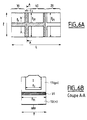
- FIG. 2A represents a top view of the component of Figure 1 and Figure 2B shows a side section view according to A-A.
- conductive channels located on either side of the guide 31, are referenced 12. The presence of these channels conductors is due to the fact that the sheath layer 11 is heavily doped.
- a lateral implantation in protons or a side etching, referenced 15 on the diagram of FIG. 2B, making the material resistive, also allows to limit the width of these channels conductors 12 at a value typically between 10 and 12 ⁇ m, and perform lateral insulation of the component.
- the conductive channels 12 prevent however obtaining a very high resistance to the interface between two sections.
- the guide wave 21 of detector 20 is for example made in ternary material, while the waveguide 31 of the laser 30 and optical insulation 40 is produced in a quantum well structure.
- metal electrodes 22, 32, 42, 13 are formed on the different sections and on the underside of the component, so that its operation.
- the second solution is to engrave the material of duct 11 in zones I located at the interfaces between sections.
- the third solution is to make a implantation of protons in the sheath material 11, locally in zones I located at the interfaces between sections.
- the protons create crystal defects that allow to reverse the type of population.
- the sheath material 11 is made locally semi-insulating and therefore highly resistive.
- the optical losses due to a proton implantation with a density of 2.10 14 cm -2 , are of the order of 0 , 8 dB for an implanted distance of 5 ⁇ m in length, which corresponds to losses of the order of 3 dB for a component having two implanted sections of 10 ⁇ m in length.
- curve a of figure 3 represents the value of the interface resistance R in function of the distance h between the bottom of the area of implantation (or engraving) I and the surface upper part of the waveguide, for a component, shown in cross-section across the Figure 3a, similar to the buried active ribbon component in Figure 1.
- This curve a shows that for reach a resistance greater than or equal to 15 k ⁇ , protons must be implanted through the waveguide (or burn), so that the bottom of the area resistive I be located at a distance h of the order of 0.8 to 0.9 ⁇ m below the upper surface of the wave guides.
- the curve b of this figure 3 represents as for it the value of the interface resistance R in function of the distance h between the bottom of the area layout (or engraving) and the upper surface of the waveguide, for a component of the prior art in which the waveguide is said to be of the "ridge" type, that is, it is not engraved.
- This component shown in cross-section across the Figure 3b, has an upper layer 14, deposited on the waveguide, which is etched across a width and over a determined length to create a contrast index and help guide the light. In this component, the waveguides are not not buried.
- An object of the present invention therefore consists in make an electro-optical monolithic component multi-sections, with buried active ribbon (waveguide BRS type), in which electrical insulation zones highly resistive I are realized, at interfaces between sections, to a sufficient depth weak so as not to reach the waveguide.
- This component must also have resistances of interface R of the same order of magnitude as those obtained with the component comprising a ribbon of the type "ridge".
- the subject of the invention is more particularly a semiconductor electro-optical monolithic component comprising at least two sections having each a first and a second guides respectively wave, said wave guides being etched in the form of tape, arranged in line and buried in a layer of sheath, and said sections being electrically isolated from each other by a resistive zone, characterized in that at the interface between two sections, the waveguides locally present a width extended at least equal to the width of the zone resistive.
- the waveguide ribbons of the different component sections so have an area locally extended allowing to locally delete the conductive channels located on either side of the waveguides, and therefore to increase the interface resistance.
- the resistive zone has a width at least equal to the conductive width of the sheath layer.
- the width sheath layer conductor is defined as being the sum of the widths of the conductive channels and of the waveguide buried in this sheath. Such a width of the resistive area allows to remove locally the lateral conductive channels and contributes obtaining sufficient electrical insulation between two sections, i.e. resistance to less than 15 k ⁇ .
- the resistive zone is obtained by local implantation of protons in the sheath layer, and has a background located at a distance of at least 0.08 ⁇ m above from the upper surface of the waveguides.
- the resistances obtained at the interfaces between the sections are very high. They are typically greater than or equal to 15 k ⁇ . These values are obtained without the electrical isolation area reaches the waveguide so that the losses optics at the interfaces between sections are greatly reduced and the operation of the electro-optical component is not disturbed.
- Figures 4A and 4B show two types of online transceiver component according to the invention, seen in longitudinal section.
- the component represented in FIG. 4A corresponds to the component of Figure 1 and the same references are used for designate the same elements.
- the only difference visible with respect to the component of the prior art, as shown schematically in Figure 1, lies in the fact that the electrical isolation zones I are made to a depth shallow enough not to reach waveguides 21 and 31 and keep them intact.
- the component represented in FIG. 4B comprises only two sections. Indeed, in this case, the laser 30 emits at a wavelength of 1.55 ⁇ m which is greater than the reception wavelength of 1.3 ⁇ m of detector 20. Detector 20 therefore remains transparent at the wavelength of 1.55 ⁇ m, and it receives correctly the signal sent to it at 1.3 ⁇ m, if although it is not necessary to place a section optically absorbent between the laser and the detector.
- the resistive zone I located at the interface between the two sections is made of so that it does not cross the waveguides 21, 31.
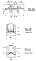
- FIGS. 5A, 5B and 5C represent the component of FIG. 4A respectively in top view and in side cuts.
- the width l I of the resistive zone I is defined along the width 1 of the component, and the length L I of the resistive zone I is defined along the length L of the component.
- the top view of FIG. 5A indicates that the waveguides 21 and 31 of the different detector 20, laser 30 and optical insulator 40 sections are engraved in the form of ribbons, but on the other hand they have a greater width at the interfaces. between sections.
- the waveguide tapes 21 and 31 locally have a width respectively l 21 and l 31 at least equal to the width l I of the resistive zone I.
- the fact of increasing the width of the guide tapes wave over the entire width of the resistive zone I locally suppresses the conductive channels which are created on either side of the ribbon and which are due to the strong doping of the sheath layer 11.
- the waveguides are locally widened, at the interface between two sections, over an overall length L 2 , L 3 preferably at least equal to the length L I of the resistive zone I.
- the overall length is defined as being the sum of the lengths of the enlarged portions of the different guides.
- the overall length L 2 of the enlarged zone corresponds to the length of the enlarged portion of the waveguide 31 added to the length of the enlarged portion from the other waveguide 21.
- the side section view according to A-A in FIG. 5B represents the waveguide 31, located at the interface, between the two laser 30 and optical insulator 40 sections.
- the waveguide ribbon 31 has at this interface an extended width l 31 equal to the width l I of the resistive zone I.
- the fact thus extending the width of the waveguide 31 makes it possible to locally remove the conductive channels 12 located on either side of the waveguide and as shown in FIG. 5C, which shows diagrammatically a sectional view, along BB, of the optical insulating section 40.
- the width of these conductive channels 12 is other part delimited by a resistive zone 15 obtained beforehand, by implantation of protons or by etching, for laterally isolating the waveguide 31.
- the width of the resistive zone l I is therefore preferably at least equal to the conductive width of the sheath layer 11, that is to say the sum of the widths of the waveguide 31 (l 31 ) and of the conductive channels 12.
- the width l I of the resistive zone is therefore delimited by the lateral insulation zones 15.
- the electrical insulation zone I can independently be obtained by proton implantation or by etching the sheath material. Because the layout, or the engraving, does not cross the waveguides, optical losses at interfaces between sections of the online transceiver according to the invention are considerably reduced.
- Figure 3 shows three comparative curves of the value of the interface resistance R as a function of the distance h between the bottom of the resistive zone I and the upper surface of the waveguide.
- the curves a and b have been described above and correspond to two multi-section components of the prior art.
- the level 0 of the distance h corresponds to the upper surface of the waveguide.
- Curve c represents the resistance values interface R obtained with a component according to the invention, shown in section in FIG. 3c, of which the waveguide ribbons are buried in a sheath layer.
- the resistance values are approximate those of the front ribbon component type "ridge". In fact, we get resistances of interface R greater than or equal to 15k ⁇ for distances h, between the bottom of the resistive zone I and the top surface of the waveguide tape at least equal to 0.08 ⁇ m.
- the invention does not only apply to the online transceiver just described. In fact, it applies, more generally, to all monolithic electro-optical components multi-sections including a buried active ribbon. She is also independent of the composition and waveguide dimensions, as well as the type of doping, n or p, of the substrate and the cladding layer.
Landscapes
- Physics & Mathematics (AREA)
- General Physics & Mathematics (AREA)
- Optics & Photonics (AREA)
- Condensed Matter Physics & Semiconductors (AREA)
- Electromagnetism (AREA)
- Engineering & Computer Science (AREA)
- Microelectronics & Electronic Packaging (AREA)
- Semiconductor Lasers (AREA)
- Optical Integrated Circuits (AREA)
- Light Receiving Elements (AREA)
Applications Claiming Priority (2)
| Application Number | Priority Date | Filing Date | Title |
|---|---|---|---|
| FR9807492 | 1998-06-15 | ||
| FR9807492A FR2779834B1 (fr) | 1998-06-15 | 1998-06-15 | Composant monolithique electro-optique multi-sections |
Publications (1)
| Publication Number | Publication Date |
|---|---|
| EP0966076A1 true EP0966076A1 (de) | 1999-12-22 |
Family
ID=9527374
Family Applications (1)
| Application Number | Title | Priority Date | Filing Date |
|---|---|---|---|
| EP99401447A Withdrawn EP0966076A1 (de) | 1998-06-15 | 1999-06-14 | Aus mehreren Abschnitten bestehendes elektrooptisches monolithisches Bauelement |
Country Status (5)
| Country | Link |
|---|---|
| US (1) | US6236794B1 (de) |
| EP (1) | EP0966076A1 (de) |
| JP (1) | JP2000031581A (de) |
| CA (1) | CA2273427A1 (de) |
| FR (1) | FR2779834B1 (de) |
Families Citing this family (2)
| Publication number | Priority date | Publication date | Assignee | Title |
|---|---|---|---|---|
| US6771682B2 (en) * | 2002-08-12 | 2004-08-03 | Infinera Corporation | Electrical isolation of optical components in photonic integrated circuits (PICs) |
| KR100576776B1 (ko) * | 2004-12-09 | 2006-05-08 | 한국전자통신연구원 | 반도체 광소자의 제작 방법 |
Citations (3)
| Publication number | Priority date | Publication date | Assignee | Title |
|---|---|---|---|---|
| JPS62291987A (ja) * | 1986-06-12 | 1987-12-18 | Mitsubishi Electric Corp | 光集積化素子 |
| EP0314490A2 (de) * | 1987-10-28 | 1989-05-03 | Kokusai Denshin Denwa Kabushiki Kaisha | Halbleiterlaser |
| EP0729042A1 (de) * | 1995-02-22 | 1996-08-28 | Alcatel N.V. | Segmentierter optischer Leiter, dessen Verwendung insbesondere in einer Halbleitervorrichtung |
-
1998
- 1998-06-15 FR FR9807492A patent/FR2779834B1/fr not_active Expired - Fee Related
-
1999
- 1999-05-31 CA CA002273427A patent/CA2273427A1/fr not_active Abandoned
- 1999-06-08 US US09/327,533 patent/US6236794B1/en not_active Expired - Lifetime
- 1999-06-14 JP JP11167390A patent/JP2000031581A/ja active Pending
- 1999-06-14 EP EP99401447A patent/EP0966076A1/de not_active Withdrawn
Patent Citations (3)
| Publication number | Priority date | Publication date | Assignee | Title |
|---|---|---|---|---|
| JPS62291987A (ja) * | 1986-06-12 | 1987-12-18 | Mitsubishi Electric Corp | 光集積化素子 |
| EP0314490A2 (de) * | 1987-10-28 | 1989-05-03 | Kokusai Denshin Denwa Kabushiki Kaisha | Halbleiterlaser |
| EP0729042A1 (de) * | 1995-02-22 | 1996-08-28 | Alcatel N.V. | Segmentierter optischer Leiter, dessen Verwendung insbesondere in einer Halbleitervorrichtung |
Non-Patent Citations (3)
| Title |
|---|
| LAMMERT R M ET AL: "INGAAS-GAAS QUANTUM-WELL LASERS WITH MONOLITHICALLY INTEGRATED INTRACAVITY ELECTROABSORPTION MODULATORS BY SELEVTIVE-AREA MOVCD", IEEE PHOTONICS TECHNOLOGY LETTERS, vol. 8, no. 1, 1 January 1996 (1996-01-01), pages 78 - 80, XP000547540 * |
| PATENT ABSTRACTS OF JAPAN vol. 012, no. 189 (E - 616) 2 June 1988 (1988-06-02) * |
| RAMDANE A ET AL: "VERY SIMPLE APPROACH FOR HIGH PERFORMANCE DFB LASER-ELECTROABSORPTION MODULATOR MONOLITHIC INTEGRATION", ELECTRONICS LETTERS, vol. 30, no. 23, 10 November 1994 (1994-11-10), pages 1980/1981, XP000495748 * |
Also Published As
| Publication number | Publication date |
|---|---|
| FR2779834B1 (fr) | 2000-08-04 |
| US6236794B1 (en) | 2001-05-22 |
| CA2273427A1 (fr) | 1999-12-15 |
| JP2000031581A (ja) | 2000-01-28 |
| FR2779834A1 (fr) | 1999-12-17 |
Similar Documents
| Publication | Publication Date | Title |
|---|---|---|
| EP0511913B1 (de) | Optoelektronisches Element mit integriertem optischem Wellenleiter und Detektor | |
| EP0645654B1 (de) | Verfahren zum Herstellen einer monolitisch integrierten Struktur mit optoelektronischen Komponenten und so hergestellte Strukturen | |
| CA2290147A1 (fr) | Composant optique a semi-conducteur comportant un adapteur de mode | |
| EP1008892A1 (de) | Halbleiterphasenmodulator | |
| EP0860724A1 (de) | Verfahren zur Herstellung eines opto-hybrides Vorrichtungs | |
| EP0240400A1 (de) | Optischer Wellenleiter aus Halbleitermaterial, Anwendung dieses Wellenleiters in einem Laser und Verfahren zu dessen Verwirklichung | |
| FR2695761A1 (fr) | Procédé de fabrication de dispositifs électro-optiques à ruban, notamment de lasers, et dispositifs ainsi obtenus. | |
| EP0752743B1 (de) | Laservorrichtung mit vergrabener Struktur für integrierte photonische Schaltung und Herstellungsverfahren | |
| FR2765347A1 (fr) | Reflecteur de bragg en semi-conducteur et procede de fabrication | |
| EP0871061A1 (de) | Wellenlängenwandler von optischen binären Signalen | |
| EP0642041B1 (de) | Aktives optisches Halbleiter-Stegwellenleiterelement | |
| EP0310184B1 (de) | Optisches Schaltelement aus zwei parallelen Lichtleitern und aus solchen Elementen zusammengesetzte Schaltmatrix | |
| FR2888405A1 (fr) | Dispositif opto-electronique comportant un laser et un modulateur integres et procede de realisation associe | |
| EP0966076A1 (de) | Aus mehreren Abschnitten bestehendes elektrooptisches monolithisches Bauelement | |
| EP0902306B1 (de) | Herstellungsverfahren eines integrierten optischen Bauteils, bestehend aus einem dicken, an einen dünnen Wellenleiter gekoppelten Wellenleiter | |
| EP0999622A1 (de) | Optische Halbleiterverstärker mit kontrolierter stabilisierter Verstärkung und optisches System unter Verwendung desselben | |
| EP0915543A1 (de) | Optische halbleiterverstärker und integrierte laserquelle | |
| CA2290142A1 (fr) | Composant optique a base d'amplificateurs optiques a semi-conducteur comportant un nombre reduit d'electrodes independantes | |
| CA2316934A1 (fr) | Composant electro-optique multi-sections | |
| WO2003043148A2 (fr) | Composant monolithique electro-optique multisections | |
| EP0992825A1 (de) | Mehrteiliger monolithischer optoelektrischer Bauelement | |
| EP0755082B1 (de) | Sender/Empfänger-Halbleitervorrichtung insbesondere für 1,3um und 1,5um | |
| FR2485823A1 (fr) | Laser semi-conducteur | |
| FR2854469A1 (fr) | Procede de fabrication d'un dispositif optique semi-conducteur comportant une region munie d'une couche active a epaisseur variable | |
| FR2683392A1 (fr) | Procede de realisation de composants optoelectroniques par epitaxie selective dans un sillon. |
Legal Events
| Date | Code | Title | Description |
|---|---|---|---|
| PUAI | Public reference made under article 153(3) epc to a published international application that has entered the european phase |
Free format text: ORIGINAL CODE: 0009012 |
|
| AK | Designated contracting states |
Kind code of ref document: A1 Designated state(s): DE GB IT SE |
|
| AX | Request for extension of the european patent |
Free format text: AL;LT;LV;MK;RO;SI |
|
| 17P | Request for examination filed |
Effective date: 20000623 |
|
| AKX | Designation fees paid |
Free format text: DE GB IT SE |
|
| 17Q | First examination report despatched |
Effective date: 20030422 |
|
| RAP1 | Party data changed (applicant data changed or rights of an application transferred) |
Owner name: AVANEX CORPORATION |
|
| RIC1 | Information provided on ipc code assigned before grant |
Ipc: 7H 01L 33/00 B Ipc: 7H 01L 27/15 B Ipc: 7G 02B 6/122 B Ipc: 7H 01S 5/06 B Ipc: 7H 01S 5/026 A |
|
| STAA | Information on the status of an ep patent application or granted ep patent |
Free format text: STATUS: THE APPLICATION IS DEEMED TO BE WITHDRAWN |
|
| 18D | Application deemed to be withdrawn |
Effective date: 20050103 |