US6153915A - CMOS semiconductor device - Google Patents
CMOS semiconductor device Download PDFInfo
- Publication number
- US6153915A US6153915A US09/070,915 US7091598A US6153915A US 6153915 A US6153915 A US 6153915A US 7091598 A US7091598 A US 7091598A US 6153915 A US6153915 A US 6153915A
- Authority
- US
- United States
- Prior art keywords
- region
- gate electrode
- impurity
- type
- semiconductor device
- Prior art date
- Legal status (The legal status is an assumption and is not a legal conclusion. Google has not performed a legal analysis and makes no representation as to the accuracy of the status listed.)
- Expired - Fee Related
Links
- 239000004065 semiconductor Substances 0.000 title claims abstract description 57
- 239000012535 impurity Substances 0.000 claims description 30
- 238000005452 bending Methods 0.000 claims 2
- 238000009792 diffusion process Methods 0.000 abstract description 24
- 238000004519 manufacturing process Methods 0.000 abstract description 12
- 230000003071 parasitic effect Effects 0.000 abstract description 7
- 230000015572 biosynthetic process Effects 0.000 description 23
- 239000000758 substrate Substances 0.000 description 17
- 238000000206 photolithography Methods 0.000 description 9
- 238000002513 implantation Methods 0.000 description 8
- VYPSYNLAJGMNEJ-UHFFFAOYSA-N Silicium dioxide Chemical compound O=[Si]=O VYPSYNLAJGMNEJ-UHFFFAOYSA-N 0.000 description 6
- 229910052814 silicon oxide Inorganic materials 0.000 description 6
- XAGFODPZIPBFFR-UHFFFAOYSA-N aluminium Chemical compound [Al] XAGFODPZIPBFFR-UHFFFAOYSA-N 0.000 description 5
- 229910052782 aluminium Inorganic materials 0.000 description 5
- 238000000034 method Methods 0.000 description 5
- ZOXJGFHDIHLPTG-UHFFFAOYSA-N Boron Chemical compound [B] ZOXJGFHDIHLPTG-UHFFFAOYSA-N 0.000 description 3
- 229910052796 boron Inorganic materials 0.000 description 3
- 230000005684 electric field Effects 0.000 description 2
- 238000010438 heat treatment Methods 0.000 description 2
- 230000010354 integration Effects 0.000 description 2
- 238000007254 oxidation reaction Methods 0.000 description 2
- 229910021420 polycrystalline silicon Inorganic materials 0.000 description 2
- 229920005591 polysilicon Polymers 0.000 description 2
- DRSFVGQMPYTGJY-GNSLJVCWSA-N Deprodone propionate Chemical compound C1CC2=CC(=O)C=C[C@]2(C)[C@@H]2[C@@H]1[C@@H]1CC[C@@](C(C)=O)(OC(=O)CC)[C@@]1(C)C[C@@H]2O DRSFVGQMPYTGJY-GNSLJVCWSA-N 0.000 description 1
- 229910052785 arsenic Inorganic materials 0.000 description 1
- RQNWIZPPADIBDY-UHFFFAOYSA-N arsenic atom Chemical compound [As] RQNWIZPPADIBDY-UHFFFAOYSA-N 0.000 description 1
- 238000010586 diagram Methods 0.000 description 1
- 230000015654 memory Effects 0.000 description 1
- 230000003647 oxidation Effects 0.000 description 1
- 229920006395 saturated elastomer Polymers 0.000 description 1
Images


Classifications
-
- H—ELECTRICITY
- H01—ELECTRIC ELEMENTS
- H01L—SEMICONDUCTOR DEVICES NOT COVERED BY CLASS H10
- H01L29/00—Semiconductor devices specially adapted for rectifying, amplifying, oscillating or switching and having potential barriers; Capacitors or resistors having potential barriers, e.g. a PN-junction depletion layer or carrier concentration layer; Details of semiconductor bodies or of electrodes thereof ; Multistep manufacturing processes therefor
- H01L29/02—Semiconductor bodies ; Multistep manufacturing processes therefor
- H01L29/06—Semiconductor bodies ; Multistep manufacturing processes therefor characterised by their shape; characterised by the shapes, relative sizes, or dispositions of the semiconductor regions ; characterised by the concentration or distribution of impurities within semiconductor regions
- H01L29/10—Semiconductor bodies ; Multistep manufacturing processes therefor characterised by their shape; characterised by the shapes, relative sizes, or dispositions of the semiconductor regions ; characterised by the concentration or distribution of impurities within semiconductor regions with semiconductor regions connected to an electrode not carrying current to be rectified, amplified or switched and such electrode being part of a semiconductor device which comprises three or more electrodes
- H01L29/107—Substrate region of field-effect devices
- H01L29/1075—Substrate region of field-effect devices of field-effect transistors
- H01L29/1079—Substrate region of field-effect devices of field-effect transistors with insulated gate
- H01L29/1087—Substrate region of field-effect devices of field-effect transistors with insulated gate characterised by the contact structure of the substrate region, e.g. for controlling or preventing bipolar effect
-
- H—ELECTRICITY
- H01—ELECTRIC ELEMENTS
- H01L—SEMICONDUCTOR DEVICES NOT COVERED BY CLASS H10
- H01L21/00—Processes or apparatus adapted for the manufacture or treatment of semiconductor or solid state devices or of parts thereof
- H01L21/70—Manufacture or treatment of devices consisting of a plurality of solid state components formed in or on a common substrate or of parts thereof; Manufacture of integrated circuit devices or of parts thereof
- H01L21/77—Manufacture or treatment of devices consisting of a plurality of solid state components or integrated circuits formed in, or on, a common substrate
- H01L21/78—Manufacture or treatment of devices consisting of a plurality of solid state components or integrated circuits formed in, or on, a common substrate with subsequent division of the substrate into plural individual devices
- H01L21/82—Manufacture or treatment of devices consisting of a plurality of solid state components or integrated circuits formed in, or on, a common substrate with subsequent division of the substrate into plural individual devices to produce devices, e.g. integrated circuits, each consisting of a plurality of components
- H01L21/822—Manufacture or treatment of devices consisting of a plurality of solid state components or integrated circuits formed in, or on, a common substrate with subsequent division of the substrate into plural individual devices to produce devices, e.g. integrated circuits, each consisting of a plurality of components the substrate being a semiconductor, using silicon technology
- H01L21/8248—Combination of bipolar and field-effect technology
- H01L21/8249—Bipolar and MOS technology
-
- H—ELECTRICITY
- H01—ELECTRIC ELEMENTS
- H01L—SEMICONDUCTOR DEVICES NOT COVERED BY CLASS H10
- H01L27/00—Devices consisting of a plurality of semiconductor or other solid-state components formed in or on a common substrate
- H01L27/02—Devices consisting of a plurality of semiconductor or other solid-state components formed in or on a common substrate including semiconductor components specially adapted for rectifying, oscillating, amplifying or switching and having potential barriers; including integrated passive circuit elements having potential barriers
- H01L27/04—Devices consisting of a plurality of semiconductor or other solid-state components formed in or on a common substrate including semiconductor components specially adapted for rectifying, oscillating, amplifying or switching and having potential barriers; including integrated passive circuit elements having potential barriers the substrate being a semiconductor body
- H01L27/06—Devices consisting of a plurality of semiconductor or other solid-state components formed in or on a common substrate including semiconductor components specially adapted for rectifying, oscillating, amplifying or switching and having potential barriers; including integrated passive circuit elements having potential barriers the substrate being a semiconductor body including a plurality of individual components in a non-repetitive configuration
- H01L27/0611—Devices consisting of a plurality of semiconductor or other solid-state components formed in or on a common substrate including semiconductor components specially adapted for rectifying, oscillating, amplifying or switching and having potential barriers; including integrated passive circuit elements having potential barriers the substrate being a semiconductor body including a plurality of individual components in a non-repetitive configuration integrated circuits having a two-dimensional layout of components without a common active region
- H01L27/0617—Devices consisting of a plurality of semiconductor or other solid-state components formed in or on a common substrate including semiconductor components specially adapted for rectifying, oscillating, amplifying or switching and having potential barriers; including integrated passive circuit elements having potential barriers the substrate being a semiconductor body including a plurality of individual components in a non-repetitive configuration integrated circuits having a two-dimensional layout of components without a common active region comprising components of the field-effect type
- H01L27/0623—Devices consisting of a plurality of semiconductor or other solid-state components formed in or on a common substrate including semiconductor components specially adapted for rectifying, oscillating, amplifying or switching and having potential barriers; including integrated passive circuit elements having potential barriers the substrate being a semiconductor body including a plurality of individual components in a non-repetitive configuration integrated circuits having a two-dimensional layout of components without a common active region comprising components of the field-effect type in combination with bipolar transistors
-
- H—ELECTRICITY
- H01—ELECTRIC ELEMENTS
- H01L—SEMICONDUCTOR DEVICES NOT COVERED BY CLASS H10
- H01L27/00—Devices consisting of a plurality of semiconductor or other solid-state components formed in or on a common substrate
- H01L27/02—Devices consisting of a plurality of semiconductor or other solid-state components formed in or on a common substrate including semiconductor components specially adapted for rectifying, oscillating, amplifying or switching and having potential barriers; including integrated passive circuit elements having potential barriers
- H01L27/04—Devices consisting of a plurality of semiconductor or other solid-state components formed in or on a common substrate including semiconductor components specially adapted for rectifying, oscillating, amplifying or switching and having potential barriers; including integrated passive circuit elements having potential barriers the substrate being a semiconductor body
- H01L27/08—Devices consisting of a plurality of semiconductor or other solid-state components formed in or on a common substrate including semiconductor components specially adapted for rectifying, oscillating, amplifying or switching and having potential barriers; including integrated passive circuit elements having potential barriers the substrate being a semiconductor body including only semiconductor components of a single kind
- H01L27/085—Devices consisting of a plurality of semiconductor or other solid-state components formed in or on a common substrate including semiconductor components specially adapted for rectifying, oscillating, amplifying or switching and having potential barriers; including integrated passive circuit elements having potential barriers the substrate being a semiconductor body including only semiconductor components of a single kind including field-effect components only
- H01L27/088—Devices consisting of a plurality of semiconductor or other solid-state components formed in or on a common substrate including semiconductor components specially adapted for rectifying, oscillating, amplifying or switching and having potential barriers; including integrated passive circuit elements having potential barriers the substrate being a semiconductor body including only semiconductor components of a single kind including field-effect components only the components being field-effect transistors with insulated gate
- H01L27/092—Devices consisting of a plurality of semiconductor or other solid-state components formed in or on a common substrate including semiconductor components specially adapted for rectifying, oscillating, amplifying or switching and having potential barriers; including integrated passive circuit elements having potential barriers the substrate being a semiconductor body including only semiconductor components of a single kind including field-effect components only the components being field-effect transistors with insulated gate complementary MIS field-effect transistors
- H01L27/0921—Means for preventing a bipolar, e.g. thyristor, action between the different transistor regions, e.g. Latchup prevention
Definitions
- the present invention relates to a semiconductor device and a method of manufacturing the same, and in particular to a semiconductor device, in which a Bi-CMOS transistor includes an n-channel MOS transistor having an improved structure, as well as a method of manufacturing the same.
- CMOS transistors which can be highly integrated and can operate with a low power consumption are now moving into the mainstream.
- demand for high-speed operation of the transistors cannot be sufficiently met at the present time, although the operation speed of MOS transistors has been increased to some extent owing to the development of miniaturizing technology.
- bipolar transistors such as an ECL are the mainstream in the field of the high-speed transistors.
- the element power consumption of the bipolar transistor is extremely large, which remarkably restricts the high integration or density.
- the Bi-CMOS transistors which can have the feature of the CMOS transistor, i.e., high integration and lower power consumption as well as the feature of the bipolar transistor, i.e., high-speed operation, have attracted the attention as the device enabling a high-speed operation with a low power consumption.
- n-type epitaxial layers 1 are formed on a p-type semiconductor substrate 10, and n + -buried layers 11 are located between p-type semiconductor substrate 10 and n-type epitaxial layers 1.
- n-type epitaxial layers 1 On the surfaces of n-type epitaxial layers 1, there are formed a bipolar transistor formation region 100 and a CMOS transistor formation region 200 which are isolated from each other by a p + -type diffusion layer 12.
- CMOS transistor formation region 200 there are formed a p-channel MOS transistor formation region 210 and an n-channel MOS transistor formation region 220.
- npn bipolar transistor 50 which includes a p-type base region 5a, an n-type collector region 6a and an n-type emitter region 6b.
- p-channel MOS transistor formation region 210 there is formed a p-channel MOS transistor 52 which includes a gate electrode 4, a p-type drain region 5b and a p-type source region 5c.
- n-channel MOS transistor formation region 220 there is formed n-channel MOS transistors 54 which includes gate electrodes 4, n-type drain regions 6c and n-type source regions 6d.
- Drain regions 6c and source regions 6d at n-channel MOS transistor formation region 220 are surrounded by a p-type back gate region 2. Further, electrode layers 9 are formed at base region 5a, emitter region 6b, collector region 6a, drain regions 5b and 6c, and source regions 5c and 6d.
- the surface of semiconductor substrate 10 is covered with a silicon oxide film 7.
- n-channel MOS transistor formation region 220 is surrounded by a field oxide film 3.
- Each gate electrode 4 is connected to a gate contact 8a via an aluminum interconnection 9b.
- An aluminum interconnection 9c is connected to back gate region 2 via back gate contact 8d.
- a method of manufacturing the Bi-CMOS transistor having the above structure will be described below with reference to FIGS. 13 to 15.
- a thin oxide film is formed on p-type semiconductor substrate 10, and then is patterned into a predetermined configuration by photolithography. Using this oxide film as a mask, n-type impurity is introduced into the surface of semiconductor substrate 10 to form n + -buried layers 11. After removing the oxide film, an epitaxial growth method is performed on semiconductor substrate 10 to form n-type epitaxial layer 1 from 4.0 to 15.0 ⁇ m in thickness.
- an oxide film having a predetermined pattern is formed on epitaxial layer 1. Using this oxide film as a mask, introduction of impurity such as boron is performed, and then heat treatment is performed to form P + -type diffusion layers 12. p-type diffusion layers 12 are continuous to substrate 10. Thereafter, p + -type back gate region 2 is formed by the steps similar to the aforementioned steps.
- an LOCOS oxidization method is performed to form silicon oxide films 3 at predetermined regions on epitaxial growth layers 1. Thereafter, polysilicon is deposited, and is patterned into a predetermined configuration by the photolithography to form gate electrodes 4.
- photolithography is performed to provide regions 5a, 5b and 5c formed from p-type impurity diffusion region, i.e., base region 5a, and drain region 5b and source region 5c of p-channel MOS transistor, as well as regions 6a, 6b, 6c and 6d formed from n-type impurity diffusion region, i.e., collector region 6a, emitter region 6b, and drain regions 6c and source regions 6d of n-channel MOS transistors. Then, silicon oxide film 7 is deposited on the uppermost surface of semiconductor substrate 10.
- Bi-CMOS transistor 500 shown in FIG. 11 is completed.
- source region 6d and back gate region 2 are set to 0 (V) (GND), 24 (V) is applied to drain region 6c, and a voltage which successively changes from 0 (V) to 24 (V) is applied to gate electrode 4.
- a current flowing from source region 6d to drain region 6c which will be referred to as a "channel current e - " is gradually increased at a strong electric field portion 14 formed near drain region 6c.
- a current flowing through drain region 6c which will be referred to as a "drain current I D ", exhibits a saturated characteristic as shown in FIGS. 17 and 18, wherein V D indicates a drain voltage and I D indicates a drain current.
- the above phenomenon or state is due to the operation of a parasitic npn bipolar transistor which is formed of drain region 6c of n-channel MOS transistor, back gate region 2 and source region 6d of n-channel MOS transistor.
- drain current (I D ) and back gate current (I BG ) in the cases where the gate electrode has a width of 7 ⁇ m as shown in FIGS. 17 and 18 and the gate electrode has a width of 500 ⁇ m as shown in FIGS. 19 and 20, the amount of holes h + flowing into back gate region 2 increases as the width (W) of gate electrode 4 increases, so that the voltage drop at back gate electrode 2 occurs further remarkably. Therefore, the parasitic bipolar transistor unavoidably operates even if the voltage applied to source region 6d and drain region 6c is small.
- the present invention has been developed to overcome the above disadvantages, and has an object to provide a semiconductor device in which operation of a parasitic bipolar transistor formed in the semiconductor device can be prevented even if a gate width is long, as well as a method of manufacturing the same.
- a semiconductor device includes a semiconductor region of a first conductivity type having a main surface, a conductive layer formed on the main surface with an insulating film therebetween and having a predetermined length and a predetermined width, a pair of first and second impurity regions of a second conductivity type formed at the main surface of the semiconductor region and having a predetermined depth, an electrode layer electrically connected to the first impurity region, and a connection layer of the first conductivity type formed at the first impurity region for electrically connecting the semiconductor region and the electrode layer together, this connection layer being formed to a depth greater than the predetermined depth of the first and second impurity regions.
- a method of manufacturing a semiconductor device according to the invention includes the following steps.
- An epitaxial layer of a second conductivity type is formed on a semiconductor substrate of a first conductivity type by an epitaxial growth method. Then, impurity of the first conductivity type is introduced into a predetermined region of the epitaxial layer to form a semiconductor region of the first conductivity type.
- a conductive layer having a predetermined length and a predetermined width is formed on a main surface of the semiconductor region with an insulating film therebetween. Thereafter, using the conductive layer as a mask, impurity of a second conductivity type is introduced into the semiconductor region to form first and second impurity regions which are located at longitudinally opposite sides of the conductive layer.
- both of the first impurity region and the semiconductor region are electrically connected to the electrode layer, so that the first impurity region and the semiconductor region are maintained at the same potential. Therefore, it is possible to suppress flow of a hole current into the semiconductor region and thus to prevent voltage drop at the semiconductor region. As a result, a potential difference between the second impurity region and the semiconductor region can be small.
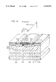
- FIG. 1 is a cross section showing a structure of a semiconductor device of a first embodiment of the invention
- FIG. 2 is a plan showing an n-channel MOS transistor formation region shown in FIG. 1;
- FIG. 3 is a cross section showing an operation of a semiconductor device according to the invention.
- FIG. 4 is a diagram showing I D -V D characteristics of the semiconductor device according to the invention.
- FIGS. 5 to 7 show 1st to 3rd steps in a method of manufacturing the semiconductor device according to the invention, respectively;
- FIG. 8 is a schematic plan showing a structure of a semiconductor device of a second embodiment of the invention.
- FIG. 9 is a schematic plan showing a structure of a third embodiment of the invention.
- FIG. 10 is a schematic plan showing a structure of a fourth embodiment of the invention.
- FIG. 11 is a cross section showing a structure of a semiconductor device in the prior art
- FIG. 12 is a plan showing an n-channel MOS transistor formation region shown in FIG. 11;
- FIGS. 13 to 15 show 1st to 3rd steps in a method of manufacturing the semiconductor device in the prior art, respectively;
- FIG. 16 is a cross section showing a structure of the semiconductor device in the prior art, and specifically showing a problem of the same;
- FIG. 17 shows I D -V D characteristics in the case where a gate width is 7 ⁇ m in the prior art
- FIG. 18 shows I BG characteristics in the case where a gate width is 7 ⁇ m in the prior art
- FIG. 19 shows I D -V D characteristics in the case where a gate width is 500 ⁇ m in the prior art.
- FIG. 20 shows I BG characteristics in the case where a gate width is 500 ⁇ m in the prior art.
- a first preferred embodiment of the invention will be described below. First, a structure of a Bi-CMOS transistor 300 of the first embodiment will be described below with reference to FIGS. 1 and 2.
- Bi-CMOS transistor 300 includes n-type epitaxial layers 1 formed on a p-type semiconductor substrate 10, and also includes n + -buried layers 11 located between p-type semiconductor substrate 10 and n-type epitaxial layers 1.
- CMOS transistor formation region 200 On the surfaces of n-type epitaxial layers 1, there are formed a bipolar transistor formation region 100 and a CMOS transistor formation region 200 which are isolated from each other by p + -type diffusion layer 12. Further, at CMOS transistor formation region 200, there are formed a p-channel MOS transistor formation region 210 and an n-channel MOS transistor formation region 220.
- npn bipolar transistor 51 which includes a p-type base region 5a, an n-type collector region 6a and an n-type emitter region 6b.
- p-channel MOS transistor formation region 210 there is formed a p-channel MOS transistor 53 which includes a gate electrode 4, a p-type drain region 5b and a p-type source region 5c.
- n-channel MOS transistor formation region 220 there is formed an n-channel MOS transistor 55 which includes gate electrode 4, n-type drain regions 6c and n-type source regions 6d. Drain regions 6c and source regions 6d of n-channel MOS transistor formation region 220 are surrounded by a p-type back gate region 2.
- electrode layers 9 are formed at base region 5a, emitter region 6b, collector region 6a, drain regions 5b and 6c, and source regions 5c and 6d.
- P + -type diffusion regions 5d for electrically connecting electrode layers 9 to back gate region 2.
- the surface of semiconductor substrate 10 is covered with a silicon oxide film 7.
- Gate electrodes 4 are disposed parallel to each other with a predetermined space therebetween. Drain contact regions 8b and source contact regions 8c are formed alternately to each other with gate electrodes 4 therebetween. Electrode layers 9 are formed at these contacts.
- n-channel MOS transistor formation region 220 is surrounded by a field oxide film 3. Each gate electrode 4 is connected to a gate contact 8a via an aluminum interconnection 9b. At each source region 6d, there is formed p + -type diffusion region 5d forming along the widthwise direction of gate electrode 4.
- n-channel MOS transistor 55 of this embodiment will be described below with reference to FIG. 3.
- p + -type diffusion region 5d is arranged at source region 6d for electrically connecting back gate region 2 and electrode layer 9 together.
- both of back gate region 2 and source region 6d are electrically connected to electrode layer 9, so that back gate region 2 and source region 6d are maintained at the same potential. Therefore, it is possible to suppress the flow of hole current into back gate region 2 and prevent voltage drop at back gate region 2, so that the potential difference between source region 6d and back gate region 2 can be reduced.
- drain voltage (V D ) is not larger than 20 (V) as shown in FIG. 4, in contrast to the prior art in which the parasitic transistor operates with drain voltage (V D ) of 12 (V) if gate electrode 4 has a width of 500 ⁇ m as shown in FIG. 19.
- Bi-CMOS transistor 300 having the above structure will be described below with reference to FIGS. 5 to 7.
- a thin oxide film is formed on p-type semiconductor substrate 10, and then is patterned into a predetermined configuration by photolithography. Using this oxide film as a mask, n-type impurity is introduced into the surface of semiconductor substrate 10 to form n + -buried layers 11. After removing the oxide film, an epitaxial growth method is performed on semiconductor substrate 10 to form n-type epitaxial layer 1 of a thickness from 4.0 to 15.0 ⁇ m.
- an oxide film having a predetermined pattern is formed on epitaxial layer 1.
- introduction of impurity such as boron is performed with the implantation energy from 50 keV to 100 keV and the implantation rate from 1.0 ⁇ 10 12 to 6.0 ⁇ 10 12 cm -2 , and the heat treatment is performed to form p + -type diffusion layers 12 and p-type back gate region 2.
- p-type diffusion layers 12 thus formed are continuous to substrate 10.
- an LOCOS oxidation method is performed to form silicon oxide films 3 having a thickness from 6000 to 16000 ⁇ at predetermined regions on epitaxial growth layers 1. Thereafter, polysilicon is deposited to form a film from 3500 to 4500 ⁇ in thickness, and is patterned into a predetermined configuration by the photolithography to form gate electrodes 4 on the gate oxide film having a thickness from 250 to 1200 ⁇ .
- photolithography is performed to provide a resist film having a predetermined pattern, and implantation of impurity such as boron is performed with the implantation rate from 1.0 ⁇ 10 14 to 3.0 ⁇ 10 14 cm -2 and implantation energy of from 50 to 60 keV to form the regions 5a, 5b and 5c and 5d formed from p-type impurity diffusion region, i.e., base region 5a, and drain region 5b and source region 5c of p-channel MOS transistor, as well as p + -type diffusion region 5d.
- impurity such as boron
- photolithography is performed to provide a resist film having a predetermined pattern
- implantation of impurity such as arsenic is performed with the implantation rate from 4.0 ⁇ 10 15 to 6.0 ⁇ 10 15 cm -2 and implantation energy of from 50 to 60 keV to form regions 6a, 6b, 6c and 6d formed from n-type impurity diffusion region, i.e., collector region 6a and emitter region 6b as well as drain regions 6c and source regions 6d of n-channel MOS transistors.
- the depth to which the p + -type diffusion region 5d is formed is greater than the depth to which the source region 6d is formed.
- Bi-CMOS transistor 300 shown in FIG. 1 is completed.
- FIG. 8 is a plan corresponding to FIG. 2, and shows a planar pattern in the case where the gate electrode is one in number.
- p + -type diffusion region 5d formed at source region 6d does not continuously forming along widthwise direction of gate electrode 4 in contrast to the first embodiment, but include several portions separated from each other.
- source region 6d has a ladder-like pattern.
- FIG. 9 is a plan corresponding to FIG. 2, and shows a planar pattern in the case where gate electrode 4 is one in number.
- p + -type diffusion region 5d formed at source region 6d does not extend linearly in the direction of the width of gate electrode 4 in contrast to the first embodiment, but include a plurality of longitudinally and laterally extending portions which have a predetermined width and is arranged continuously to form a zigzag form.
- FIG. 10 is a plan corresponding to FIG. 2, and shows a planar pattern in the case where the gate electrode is one in number.
- p + -type diffusion region 5d formed at source region 6d does not continuously extend widthwise of gate electrode 4 in contrast to the first embodiment, but include a plurality of portions which extend perpendicularly to gate electrode 4 and is spaced from each other by a predetermined distance.
- source contact 8c can be formed at an arbitrary position without taking the disposition of p + -type diffusion region 5d into consideration. Further, even if a mask is dislocated at the step for forming the source contact hole, the contact to p + -type diffusion region 5d can be surely made, so that it is not necessary to take the dislocation of the mask for the source contact hole into consideration.
- connection layer of the first conductivity type for electrically connecting the back gate region and the electrode layer together is formed at the source region.
- the potential difference between the drain region and the back gate region can be small, so that, even if the gate electrode has a large width, it is possible to suppress the operation of the parasitic bipolar transistor and thus to provide the semiconductor device having high reliability.
Landscapes
- Engineering & Computer Science (AREA)
- Power Engineering (AREA)
- Microelectronics & Electronic Packaging (AREA)
- Physics & Mathematics (AREA)
- Condensed Matter Physics & Semiconductors (AREA)
- General Physics & Mathematics (AREA)
- Computer Hardware Design (AREA)
- Manufacturing & Machinery (AREA)
- Ceramic Engineering (AREA)
- Metal-Oxide And Bipolar Metal-Oxide Semiconductor Integrated Circuits (AREA)
- Electrodes Of Semiconductors (AREA)
- Insulated Gate Type Field-Effect Transistor (AREA)
Abstract
In a semiconductor device and a method of manufacturing the same according to the invention, a p-type diffusion region for electrically connecting a back gate region and an electrode layer together is formed at a source region. Thereby, both of source region and p-type diffusion region are electrically connected to the electrode layer, so that the source region and the back gate region are maintained at the same potential. As a result, it is possible to provide the semiconductor device and the method of manufacturing the same which can suppress operation of a parasitic bipolar transistor formed in the semiconductor device even if a gate electrode has a large width.
Description
This application is a continuation of application Ser. No. 08/742,120 filed Oct. 31, 1996, now U.S. Pat. No. 5,763,926, which is a continuation of application Ser. No. 08/551,393 filed Nov. 1, 1995, now abandoned, which is a continuation of application Ser. No. 08/333,990 filed Nov. 2, 1994, now abandoned.
1. Field of the Invention
The present invention relates to a semiconductor device and a method of manufacturing the same, and in particular to a semiconductor device, in which a Bi-CMOS transistor includes an n-channel MOS transistor having an improved structure, as well as a method of manufacturing the same.
2. Description of the Background Art
In recent years, it has been attempted to increase a scale of VLSIs such as memories and processors. For complying with the demand for increase of the scale, CMOS transistors which can be highly integrated and can operate with a low power consumption are now moving into the mainstream. However, demand for high-speed operation of the transistors cannot be sufficiently met at the present time, although the operation speed of MOS transistors has been increased to some extent owing to the development of miniaturizing technology. In general, bipolar transistors such as an ECL are the mainstream in the field of the high-speed transistors. However, the element power consumption of the bipolar transistor is extremely large, which remarkably restricts the high integration or density. In view of the aforementioned background, the Bi-CMOS transistors, which can have the feature of the CMOS transistor, i.e., high integration and lower power consumption as well as the feature of the bipolar transistor, i.e., high-speed operation, have attracted the attention as the device enabling a high-speed operation with a low power consumption.
Then, a structure of the conventional Bi-CMOS transistor will be described below with reference to FIG. 11. In a Bi-CMOS transistor 500, n-type epitaxial layers 1 are formed on a p-type semiconductor substrate 10, and n+ -buried layers 11 are located between p-type semiconductor substrate 10 and n-type epitaxial layers 1. On the surfaces of n-type epitaxial layers 1, there are formed a bipolar transistor formation region 100 and a CMOS transistor formation region 200 which are isolated from each other by a p+ -type diffusion layer 12. Further, at each CMOS transistor formation region 200, there are formed a p-channel MOS transistor formation region 210 and an n-channel MOS transistor formation region 220.
At bipolar transistor formation region 100, there is formed an npn bipolar transistor 50 which includes a p-type base region 5a, an n-type collector region 6a and an n-type emitter region 6b. At p-channel MOS transistor formation region 210, there is formed a p-channel MOS transistor 52 which includes a gate electrode 4, a p-type drain region 5b and a p-type source region 5c. At n-channel MOS transistor formation region 220, there is formed n-channel MOS transistors 54 which includes gate electrodes 4, n-type drain regions 6c and n-type source regions 6d.
Then, a planar pattern of n-channel MOS transistor formation region 220 will be described below with reference to FIG. 12. Gate electrodes 4 are disposed parallel to each other with a predetermined space therebetween. Drain contact regions 8b and source contact regions 8c are formed alternately to each other between gate electrodes 4. Electrode layers 9 are formed at these contact regions. n-channel MOS transistor formation region 220 is surrounded by a field oxide film 3. Each gate electrode 4 is connected to a gate contact 8a via an aluminum interconnection 9b. An aluminum interconnection 9c is connected to back gate region 2 via back gate contact 8d.
A method of manufacturing the Bi-CMOS transistor having the above structure will be described below with reference to FIGS. 13 to 15. Referring first to FIG. 13, a thin oxide film is formed on p-type semiconductor substrate 10, and then is patterned into a predetermined configuration by photolithography. Using this oxide film as a mask, n-type impurity is introduced into the surface of semiconductor substrate 10 to form n+ -buried layers 11. After removing the oxide film, an epitaxial growth method is performed on semiconductor substrate 10 to form n-type epitaxial layer 1 from 4.0 to 15.0 μm in thickness.
Similarly to the aforementioned step, an oxide film having a predetermined pattern is formed on epitaxial layer 1. Using this oxide film as a mask, introduction of impurity such as boron is performed, and then heat treatment is performed to form P+ -type diffusion layers 12. p-type diffusion layers 12 are continuous to substrate 10. Thereafter, p+ -type back gate region 2 is formed by the steps similar to the aforementioned steps.
Referring to FIG. 14, an LOCOS oxidization method is performed to form silicon oxide films 3 at predetermined regions on epitaxial growth layers 1. Thereafter, polysilicon is deposited, and is patterned into a predetermined configuration by the photolithography to form gate electrodes 4.
Referring to FIG. 15, photolithography is performed to provide regions 5a, 5b and 5c formed from p-type impurity diffusion region, i.e., base region 5a, and drain region 5b and source region 5c of p-channel MOS transistor, as well as regions 6a, 6b, 6c and 6d formed from n-type impurity diffusion region, i.e., collector region 6a, emitter region 6b, and drain regions 6c and source regions 6d of n-channel MOS transistors. Then, silicon oxide film 7 is deposited on the uppermost surface of semiconductor substrate 10. Thereafter, photolithography is performed to form contact holes communicated with base region 5a, collector region 6a, emitter region 6b, drain regions 5b and 6c, and source regions 5c and 6d. Then, insulating layers 9, e.g., made of aluminum are formed. In this manner, Bi-CMOS transistor 500 shown in FIG. 11 is completed.
The following problem, however, exists in the prior art described above. First, referring to FIG. 16, source region 6d and back gate region 2 are set to 0 (V) (GND), 24 (V) is applied to drain region 6c, and a voltage which successively changes from 0 (V) to 24 (V) is applied to gate electrode 4. In this operation, a current flowing from source region 6d to drain region 6c, which will be referred to as a "channel current e- " is gradually increased at a strong electric field portion 14 formed near drain region 6c. When the voltage of 24 (V) is applied to drain region 6c, a current flowing through drain region 6c, which will be referred to as a "drain current ID ", exhibits a saturated characteristic as shown in FIGS. 17 and 18, wherein VD indicates a drain voltage and ID indicates a drain current.
The reason of the above phenomenon or state is that channel current e- is increased at strong electric field portion 14 near drain region 6c, so that the amount of holes h+ flowing into back gate region 2 remarkably increases, resulting in increase of the current flowing through back gate region 2, which will be referred to as a "back gate current". Therefore, voltage drop occurs at back gate region 2, so that a forward bias is applied across source region 6d and back gate region 2.
Thus, the above phenomenon or state is due to the operation of a parasitic npn bipolar transistor which is formed of drain region 6c of n-channel MOS transistor, back gate region 2 and source region 6d of n-channel MOS transistor. As can be seen from comparison of drain current (ID) and back gate current (IBG) in the cases where the gate electrode has a width of 7 μm as shown in FIGS. 17 and 18 and the gate electrode has a width of 500 μm as shown in FIGS. 19 and 20, the amount of holes h+ flowing into back gate region 2 increases as the width (W) of gate electrode 4 increases, so that the voltage drop at back gate electrode 2 occurs further remarkably. Therefore, the parasitic bipolar transistor unavoidably operates even if the voltage applied to source region 6d and drain region 6c is small.
The present invention has been developed to overcome the above disadvantages, and has an object to provide a semiconductor device in which operation of a parasitic bipolar transistor formed in the semiconductor device can be prevented even if a gate width is long, as well as a method of manufacturing the same.
In order to achieve the above object, a semiconductor device according to the invention includes a semiconductor region of a first conductivity type having a main surface, a conductive layer formed on the main surface with an insulating film therebetween and having a predetermined length and a predetermined width, a pair of first and second impurity regions of a second conductivity type formed at the main surface of the semiconductor region and having a predetermined depth, an electrode layer electrically connected to the first impurity region, and a connection layer of the first conductivity type formed at the first impurity region for electrically connecting the semiconductor region and the electrode layer together, this connection layer being formed to a depth greater than the predetermined depth of the first and second impurity regions.
In order to achieve the above object, a method of manufacturing a semiconductor device according to the invention includes the following steps.
An epitaxial layer of a second conductivity type is formed on a semiconductor substrate of a first conductivity type by an epitaxial growth method. Then, impurity of the first conductivity type is introduced into a predetermined region of the epitaxial layer to form a semiconductor region of the first conductivity type.
A conductive layer having a predetermined length and a predetermined width is formed on a main surface of the semiconductor region with an insulating film therebetween. Thereafter, using the conductive layer as a mask, impurity of a second conductivity type is introduced into the semiconductor region to form first and second impurity regions which are located at longitudinally opposite sides of the conductive layer.
According to the semiconductor device and the method of manufacturing the same described above, both of the first impurity region and the semiconductor region are electrically connected to the electrode layer, so that the first impurity region and the semiconductor region are maintained at the same potential. Therefore, it is possible to suppress flow of a hole current into the semiconductor region and thus to prevent voltage drop at the semiconductor region. As a result, a potential difference between the second impurity region and the semiconductor region can be small.
The foregoing and other objects, features, aspects and advantages of the present invention will become more apparent from the following detailed description of the present invention when taken in conjunction with the accompanying drawings.
FIG. 1 is a cross section showing a structure of a semiconductor device of a first embodiment of the invention;
FIG. 2 is a plan showing an n-channel MOS transistor formation region shown in FIG. 1;
FIG. 3 is a cross section showing an operation of a semiconductor device according to the invention;
FIG. 4 is a diagram showing ID -VD characteristics of the semiconductor device according to the invention;
FIGS. 5 to 7 show 1st to 3rd steps in a method of manufacturing the semiconductor device according to the invention, respectively;
FIG. 8 is a schematic plan showing a structure of a semiconductor device of a second embodiment of the invention;
FIG. 9 is a schematic plan showing a structure of a third embodiment of the invention;
FIG. 10 is a schematic plan showing a structure of a fourth embodiment of the invention;
FIG. 11 is a cross section showing a structure of a semiconductor device in the prior art;
FIG. 12 is a plan showing an n-channel MOS transistor formation region shown in FIG. 11;
FIGS. 13 to 15 show 1st to 3rd steps in a method of manufacturing the semiconductor device in the prior art, respectively;
FIG. 16 is a cross section showing a structure of the semiconductor device in the prior art, and specifically showing a problem of the same;
FIG. 17 shows ID -VD characteristics in the case where a gate width is 7 μm in the prior art;
FIG. 18 shows IBG characteristics in the case where a gate width is 7 μm in the prior art;
FIG. 19 shows ID -VD characteristics in the case where a gate width is 500 μm in the prior art; and
FIG. 20 shows IBG characteristics in the case where a gate width is 500 μm in the prior art.
A first preferred embodiment of the invention will be described below. First, a structure of a Bi-CMOS transistor 300 of the first embodiment will be described below with reference to FIGS. 1 and 2.
Referring first to FIG. 1, Bi-CMOS transistor 300 includes n-type epitaxial layers 1 formed on a p-type semiconductor substrate 10, and also includes n+ -buried layers 11 located between p-type semiconductor substrate 10 and n-type epitaxial layers 1.
On the surfaces of n-type epitaxial layers 1, there are formed a bipolar transistor formation region 100 and a CMOS transistor formation region 200 which are isolated from each other by p+ -type diffusion layer 12. Further, at CMOS transistor formation region 200, there are formed a p-channel MOS transistor formation region 210 and an n-channel MOS transistor formation region 220.
At bipolar transistor formation region 100, there is formed an npn bipolar transistor 51 which includes a p-type base region 5a, an n-type collector region 6a and an n-type emitter region 6b. At p-channel MOS transistor formation region 210, there is formed a p-channel MOS transistor 53 which includes a gate electrode 4, a p-type drain region 5b and a p-type source region 5c. At n-channel MOS transistor formation region 220, there is formed an n-channel MOS transistor 55 which includes gate electrode 4, n-type drain regions 6c and n-type source regions 6d. Drain regions 6c and source regions 6d of n-channel MOS transistor formation region 220 are surrounded by a p-type back gate region 2.
Further, electrode layers 9 are formed at base region 5a, emitter region 6b, collector region 6a, drain regions 5b and 6c, and source regions 5c and 6d. At each source region 6d, there is provided P+ -type diffusion regions 5d for electrically connecting electrode layers 9 to back gate region 2. The surface of semiconductor substrate 10 is covered with a silicon oxide film 7.
Then, a planar pattern of the n-channel MOS transistor will be described below with reference to FIG. 2. Gate electrodes 4 are disposed parallel to each other with a predetermined space therebetween. Drain contact regions 8b and source contact regions 8c are formed alternately to each other with gate electrodes 4 therebetween. Electrode layers 9 are formed at these contacts. n-channel MOS transistor formation region 220 is surrounded by a field oxide film 3. Each gate electrode 4 is connected to a gate contact 8a via an aluminum interconnection 9b. At each source region 6d, there is formed p+ -type diffusion region 5d forming along the widthwise direction of gate electrode 4.
Operation of n-channel MOS transistor 55 of this embodiment will be described below with reference to FIG. 3. In this embodiment, p+ -type diffusion region 5d is arranged at source region 6d for electrically connecting back gate region 2 and electrode layer 9 together. Thereby, both of back gate region 2 and source region 6d are electrically connected to electrode layer 9, so that back gate region 2 and source region 6d are maintained at the same potential. Therefore, it is possible to suppress the flow of hole current into back gate region 2 and prevent voltage drop at back gate region 2, so that the potential difference between source region 6d and back gate region 2 can be reduced.
As a result, it is possible to prevent operation of the parasitic bipolar transistor if drain voltage (VD) is not larger than 20 (V) as shown in FIG. 4, in contrast to the prior art in which the parasitic transistor operates with drain voltage (VD) of 12 (V) if gate electrode 4 has a width of 500 μm as shown in FIG. 19.
A method of manufacturing Bi-CMOS transistor 300 having the above structure will be described below with reference to FIGS. 5 to 7. Referring first to FIG. 5, a thin oxide film is formed on p-type semiconductor substrate 10, and then is patterned into a predetermined configuration by photolithography. Using this oxide film as a mask, n-type impurity is introduced into the surface of semiconductor substrate 10 to form n+ -buried layers 11. After removing the oxide film, an epitaxial growth method is performed on semiconductor substrate 10 to form n-type epitaxial layer 1 of a thickness from 4.0 to 15.0 μm.
Similarly to the aforementioned step, an oxide film having a predetermined pattern is formed on epitaxial layer 1. Using this oxide film as a mask, introduction of impurity such as boron is performed with the implantation energy from 50 keV to 100 keV and the implantation rate from 1.0×10¹² to 6.0×1012 cm-2, and the heat treatment is performed to form p+ -type diffusion layers 12 and p-type back gate region 2. p-type diffusion layers 12 thus formed are continuous to substrate 10.
Referring to FIG. 6, an LOCOS oxidation method is performed to form silicon oxide films 3 having a thickness from 6000 to 16000 Å at predetermined regions on epitaxial growth layers 1. Thereafter, polysilicon is deposited to form a film from 3500 to 4500 Å in thickness, and is patterned into a predetermined configuration by the photolithography to form gate electrodes 4 on the gate oxide film having a thickness from 250 to 1200 Å.
Referring to FIG. 7, photolithography is performed to provide a resist film having a predetermined pattern, and implantation of impurity such as boron is performed with the implantation rate from 1.0×10¹⁴ to 3.0×1014 cm-2 and implantation energy of from 50 to 60 keV to form the regions 5a, 5b and 5c and 5d formed from p-type impurity diffusion region, i.e., base region 5a, and drain region 5b and source region 5c of p-channel MOS transistor, as well as p+ -type diffusion region 5d. Further, photolithography is performed to provide a resist film having a predetermined pattern, and implantation of impurity such as arsenic is performed with the implantation rate from 4.0×10¹⁵ to 6.0×1015 cm-2 and implantation energy of from 50 to 60 keV to form regions 6a, 6b, 6c and 6d formed from n-type impurity diffusion region, i.e., collector region 6a and emitter region 6b as well as drain regions 6c and source regions 6d of n-channel MOS transistors.
As clearly shown in FIGS. 1 and 7, and particularly in FIG. 3, the depth to which the p+ -type diffusion region 5d is formed is greater than the depth to which the source region 6d is formed.
Then, silicon oxide film 7 is deposited on the surface of semiconductor substrate 10. Thereafter, photolithography is performed to form contact holes communicated with base region 5a, collector region 6a, emitter region 6b, drain regions 5b and 6c, source regions 5c and 6d, and insulating layers 9, e.g., made of aluminum are formed. In this manner, Bi-CMOS transistor 300 shown in FIG. 1 is completed.
A second embodiment according to the invention will be described below with reference to FIG. 8. FIG. 8 is a plan corresponding to FIG. 2, and shows a planar pattern in the case where the gate electrode is one in number. According to this embodiment, p+ -type diffusion region 5d formed at source region 6d does not continuously forming along widthwise direction of gate electrode 4 in contrast to the first embodiment, but include several portions separated from each other. Thus, source region 6d has a ladder-like pattern.
Owing to this structure, contact between source region 6d and p+ -type diffusion region 5d is ensured even if a width (SW) of source contact 8c is further reduced, so that a planar area of the semiconductor device can be reduced.
Then, a third embodiment according to the invention will be described below with reference to FIG. 9. FIG. 9 is a plan corresponding to FIG. 2, and shows a planar pattern in the case where gate electrode 4 is one in number. According to this embodiment, p+ -type diffusion region 5d formed at source region 6d does not extend linearly in the direction of the width of gate electrode 4 in contrast to the first embodiment, but include a plurality of longitudinally and laterally extending portions which have a predetermined width and is arranged continuously to form a zigzag form.
Owing to this structure, even if a mask for forming source contact 8c is dislocated or shifted, p+ -type diffusion region 5d is surely formed at source contact 8c, so that reliability of the semiconductor device can be improved.
A fourth embodiment according to this embodiment will be described below with reference to FIG. 10. FIG. 10 is a plan corresponding to FIG. 2, and shows a planar pattern in the case where the gate electrode is one in number. According to this embodiment, p+ -type diffusion region 5d formed at source region 6d does not continuously extend widthwise of gate electrode 4 in contrast to the first embodiment, but include a plurality of portions which extend perpendicularly to gate electrode 4 and is spaced from each other by a predetermined distance.
Owing to this structure, source contact 8c can be formed at an arbitrary position without taking the disposition of p+ -type diffusion region 5d into consideration. Further, even if a mask is dislocated at the step for forming the source contact hole, the contact to p+ -type diffusion region 5d can be surely made, so that it is not necessary to take the dislocation of the mask for the source contact hole into consideration.
In the semiconductor device and the method of manufacturing the same according to the invention, the connection layer of the first conductivity type for electrically connecting the back gate region and the electrode layer together is formed at the source region. Thereby, both of the source region and the back gate region are electrically connected to the electrode layer, so that the back gate region and the source region are maintained at the same potential.
Therefore, it is possible to suppress the flow of the hole current into the back gate region, and thus to prevent the voltage drop at the back gate region. As a result, the potential difference between the drain region and the back gate region can be small, so that, even if the gate electrode has a large width, it is possible to suppress the operation of the parasitic bipolar transistor and thus to provide the semiconductor device having high reliability.
Although the present invention has been described and illustrated in detail, it is clearly understood that the same is by way of illustration and example only and is not to be taken by way of limitation, the spirit and scope of the present invention being limited only by the terms of the appended claims.
Claims (2)
1. A semiconductor device, comprising:
a semiconductor region of a first conductivity type having a main surface;
a gate electrode formed on said main surface with an insulating film therebetween and having a predetermined length;
a pair of first and second impurity regions of a second conductivity type formed at said main surface of said semiconductor region to a predetermined depth, said first and second impurity regions extending in the gate electrode width direction;
an electrode layer electrically connected to said first impurity region at a surface contact region and spaced apart from a side surface of the gate electrode extending in the gate width direction; and
a connection layer of the first conductivity type formed at said first impurity region for electrically connecting said semiconductor region and said electrode layer, wherein the distance between the side surface of the gate electrode and the connection layer in the gate electrode length direction changes abruptly at least once along the gate electrode width direction; the gate electrode extends linearly without a bending portion across said first and second impurity regions in plan view; and said connection layer is arranged in a zigzag form.
2. A semiconductor device, comprising:
a semiconductor region of a first conductivity type having a main surface;
a gate electrode formed on said main surface with an insulating film therebetween and having a predetermined length;
a pair of first and second impurity regions of a second conductivity type formed at said main surface of said semiconductor region to a predetermined depth, said first and second impurity regions extending in the gate electrode width direction;
an electrode layer electrically connected to said first impurity region at a surface contact region and spaced apart from a side surface of the gate electrode extending in the gate width direction; and
a connection layer of the first conductivity type formed at said first impurity region for electrically connecting said semiconductor region and said electrode layer, wherein the distance between the side surface of the gate electrode and the connection layer in the gate electrode length direction changes abruptly at least once along the gate electrode width direction, wherein only two side surfaces of the gate electrode extend linearly without a bending portion across said first and second impurity regions in plan view wherein;
said connection layer is arranged to form a continuous zigzag form.
Priority Applications (1)
| Application Number | Priority Date | Filing Date | Title |
|---|---|---|---|
| US09/070,915 US6153915A (en) | 1993-11-05 | 1998-05-04 | CMOS semiconductor device |
Applications Claiming Priority (6)
| Application Number | Priority Date | Filing Date | Title |
|---|---|---|---|
| JP27668593A JP3307481B2 (en) | 1993-11-05 | 1993-11-05 | Semiconductor device |
| JP5-276685 | 1993-11-05 | ||
| US33399094A | 1994-11-02 | 1994-11-02 | |
| US55139395A | 1995-11-01 | 1995-11-01 | |
| US08/742,120 US5763926A (en) | 1993-11-05 | 1996-10-31 | Semiconductor device having a Bi-CMOS transistor including an n-channel MOS transistor |
| US09/070,915 US6153915A (en) | 1993-11-05 | 1998-05-04 | CMOS semiconductor device |
Related Parent Applications (1)
| Application Number | Title | Priority Date | Filing Date |
|---|---|---|---|
| US08/742,120 Continuation US5763926A (en) | 1993-11-05 | 1996-10-31 | Semiconductor device having a Bi-CMOS transistor including an n-channel MOS transistor |
Publications (1)
| Publication Number | Publication Date |
|---|---|
| US6153915A true US6153915A (en) | 2000-11-28 |
Family
ID=17572898
Family Applications (2)
| Application Number | Title | Priority Date | Filing Date |
|---|---|---|---|
| US08/742,120 Expired - Fee Related US5763926A (en) | 1993-11-05 | 1996-10-31 | Semiconductor device having a Bi-CMOS transistor including an n-channel MOS transistor |
| US09/070,915 Expired - Fee Related US6153915A (en) | 1993-11-05 | 1998-05-04 | CMOS semiconductor device |
Family Applications Before (1)
| Application Number | Title | Priority Date | Filing Date |
|---|---|---|---|
| US08/742,120 Expired - Fee Related US5763926A (en) | 1993-11-05 | 1996-10-31 | Semiconductor device having a Bi-CMOS transistor including an n-channel MOS transistor |
Country Status (3)
| Country | Link |
|---|---|
| US (2) | US5763926A (en) |
| JP (1) | JP3307481B2 (en) |
| DE (1) | DE4439131C2 (en) |
Cited By (1)
| Publication number | Priority date | Publication date | Assignee | Title |
|---|---|---|---|---|
| US20090050978A1 (en) * | 2006-03-31 | 2009-02-26 | Naohiro Ueda | Semiconductor device |
Families Citing this family (4)
| Publication number | Priority date | Publication date | Assignee | Title |
|---|---|---|---|---|
| JP3307481B2 (en) * | 1993-11-05 | 2002-07-24 | 三菱電機株式会社 | Semiconductor device |
| TWI361490B (en) | 2003-09-05 | 2012-04-01 | Renesas Electronics Corp | A semiconductor device and a method of manufacturing the same |
| KR100541656B1 (en) * | 2004-08-03 | 2006-01-11 | 삼성전자주식회사 | Cmos device with improved performance and fabrication method thereof |
| JP5585593B2 (en) * | 2010-01-29 | 2014-09-10 | 富士電機株式会社 | Semiconductor device |
Citations (8)
| Publication number | Priority date | Publication date | Assignee | Title |
|---|---|---|---|---|
| US4035826A (en) * | 1976-02-23 | 1977-07-12 | Rca Corporation | Reduction of parasitic bipolar effects in integrated circuits employing insulated gate field effect transistors via the use of low resistance substrate contacts extending through source region |
| JPS5422781A (en) * | 1977-07-22 | 1979-02-20 | Hitachi Ltd | Insulator gate protective semiconductor device |
| JPS5688363A (en) * | 1979-12-20 | 1981-07-17 | Nec Corp | Field effect transistor |
| US4614959A (en) * | 1979-12-10 | 1986-09-30 | Sharp Kabushiki Kaisha | Improved high voltage MOS transistor with field plate layers for preventing reverse field plate effect |
| DE3414772C2 (en) * | 1983-04-25 | 1987-10-08 | Mitsubishi Denki K.K., Tokio/Tokyo, Jp | |
| US5274259A (en) * | 1993-02-01 | 1993-12-28 | Power Integrations, Inc. | High voltage transistor |
| US5319236A (en) * | 1991-07-19 | 1994-06-07 | Fuji Electric Co., Ltd. | Semiconductor device equipped with a high-voltage MISFET |
| US5763926A (en) * | 1993-11-05 | 1998-06-09 | Mitsubishi Denki Kabushiki Kaisha | Semiconductor device having a Bi-CMOS transistor including an n-channel MOS transistor |
-
1993
- 1993-11-05 JP JP27668593A patent/JP3307481B2/en not_active Expired - Fee Related
-
1994
- 1994-11-02 DE DE4439131A patent/DE4439131C2/en not_active Expired - Fee Related
-
1996
- 1996-10-31 US US08/742,120 patent/US5763926A/en not_active Expired - Fee Related
-
1998
- 1998-05-04 US US09/070,915 patent/US6153915A/en not_active Expired - Fee Related
Patent Citations (8)
| Publication number | Priority date | Publication date | Assignee | Title |
|---|---|---|---|---|
| US4035826A (en) * | 1976-02-23 | 1977-07-12 | Rca Corporation | Reduction of parasitic bipolar effects in integrated circuits employing insulated gate field effect transistors via the use of low resistance substrate contacts extending through source region |
| JPS5422781A (en) * | 1977-07-22 | 1979-02-20 | Hitachi Ltd | Insulator gate protective semiconductor device |
| US4614959A (en) * | 1979-12-10 | 1986-09-30 | Sharp Kabushiki Kaisha | Improved high voltage MOS transistor with field plate layers for preventing reverse field plate effect |
| JPS5688363A (en) * | 1979-12-20 | 1981-07-17 | Nec Corp | Field effect transistor |
| DE3414772C2 (en) * | 1983-04-25 | 1987-10-08 | Mitsubishi Denki K.K., Tokio/Tokyo, Jp | |
| US5319236A (en) * | 1991-07-19 | 1994-06-07 | Fuji Electric Co., Ltd. | Semiconductor device equipped with a high-voltage MISFET |
| US5274259A (en) * | 1993-02-01 | 1993-12-28 | Power Integrations, Inc. | High voltage transistor |
| US5763926A (en) * | 1993-11-05 | 1998-06-09 | Mitsubishi Denki Kabushiki Kaisha | Semiconductor device having a Bi-CMOS transistor including an n-channel MOS transistor |
Non-Patent Citations (2)
| Title |
|---|
| IEEE Electron Device Letters, "Failure in CMOS Circuits Induced by Hot Carriers in Multi-Gate Transistors", vol. 9, No. 11, 1988, pp. 564-566. |
| IEEE Electron Device Letters, Failure in CMOS Circuits Induced by Hot Carriers in Multi Gate Transistors , vol. 9, No. 11, 1988, pp. 564 566. * |
Cited By (1)
| Publication number | Priority date | Publication date | Assignee | Title |
|---|---|---|---|---|
| US20090050978A1 (en) * | 2006-03-31 | 2009-02-26 | Naohiro Ueda | Semiconductor device |
Also Published As
| Publication number | Publication date |
|---|---|
| DE4439131A1 (en) | 1995-05-11 |
| JP3307481B2 (en) | 2002-07-24 |
| US5763926A (en) | 1998-06-09 |
| JPH07130898A (en) | 1995-05-19 |
| DE4439131C2 (en) | 1998-02-19 |
Similar Documents
| Publication | Publication Date | Title |
|---|---|---|
| JP2950558B2 (en) | Semiconductor device | |
| JP3364559B2 (en) | Semiconductor device | |
| US6171905B1 (en) | Semiconductor device and method of manufacturing the same | |
| US5945712A (en) | Semiconductor device having a SOI structure with substrate bias formed through the insulator and in contact with one of the active diffusion layers | |
| US5371401A (en) | Semiconductor integrated circuit fully isolated from the substrate | |
| EP0217288A2 (en) | Substrate structure for a composite semiconductor device | |
| US7964457B2 (en) | Semiconductor integrated circuit device and a manufacturing method for the same | |
| JP2991489B2 (en) | Semiconductor device | |
| JP3400891B2 (en) | Semiconductor storage device and method of manufacturing the same | |
| KR19980066427A (en) | Semiconductor device and manufacturing method thereof | |
| US6153915A (en) | CMOS semiconductor device | |
| KR890004797B1 (en) | Mis type semiconductor device element on a semiconductor substrate having a well region | |
| JP4145353B2 (en) | Semiconductor device provided with a resistance element | |
| US5583363A (en) | Inverter gate circuit of a bi-CMOS structure having common layers between fets and bipolar transistors | |
| US4819055A (en) | Semiconductor device having a PN junction formed on an insulator film | |
| JP2000049237A (en) | Semiconductor device and its manufacture | |
| JPH02246264A (en) | Semiconductor device and manufacture thereof | |
| KR900007904B1 (en) | Method of manufacturing semiconductor device | |
| JP2919494B2 (en) | Vertical MOSFET | |
| US4622571A (en) | CMOS integrated circuit device | |
| US5866921A (en) | Lateral SRAM transistor circuits and methods of fabrication therefor | |
| US7091617B2 (en) | Design and layout techniques for low parasitic capacitance in analog circuit applications | |
| JP4003981B2 (en) | Semiconductor device | |
| US4990461A (en) | Method of making a semiconductor integrated circuit device having resistance elements | |
| JP3361615B2 (en) | Ferroelectric element |
Legal Events
| Date | Code | Title | Description |
|---|---|---|---|
| FEPP | Fee payment procedure |
Free format text: PAYOR NUMBER ASSIGNED (ORIGINAL EVENT CODE: ASPN); ENTITY STATUS OF PATENT OWNER: LARGE ENTITY |
|
| FPAY | Fee payment |
Year of fee payment: 4 |
|
| REMI | Maintenance fee reminder mailed | ||
| LAPS | Lapse for failure to pay maintenance fees | ||
| STCH | Information on status: patent discontinuation |
Free format text: PATENT EXPIRED DUE TO NONPAYMENT OF MAINTENANCE FEES UNDER 37 CFR 1.362 |
|
| FP | Lapsed due to failure to pay maintenance fee |
Effective date: 20081128 |