JP5585593B2 - Semiconductor device - Google Patents
Semiconductor device Download PDFInfo
- Publication number
- JP5585593B2 JP5585593B2 JP2011551945A JP2011551945A JP5585593B2 JP 5585593 B2 JP5585593 B2 JP 5585593B2 JP 2011551945 A JP2011551945 A JP 2011551945A JP 2011551945 A JP2011551945 A JP 2011551945A JP 5585593 B2 JP5585593 B2 JP 5585593B2
- Authority
- JP
- Japan
- Prior art keywords
- layer
- concentration
- protective diode
- diode
- semiconductor
- Prior art date
- Legal status (The legal status is an assumption and is not a legal conclusion. Google has not performed a legal analysis and makes no representation as to the accuracy of the status listed.)
- Expired - Fee Related
Links
- 239000004065 semiconductor Substances 0.000 title claims description 330
- 230000001681 protective effect Effects 0.000 claims description 201
- 239000000758 substrate Substances 0.000 claims description 29
- 230000002457 bidirectional effect Effects 0.000 claims description 23
- 229910021420 polycrystalline silicon Inorganic materials 0.000 claims description 14
- 229920005591 polysilicon Polymers 0.000 claims description 13
- 229910021421 monocrystalline silicon Inorganic materials 0.000 claims description 4
- 239000010410 layer Substances 0.000 description 454
- 230000015556 catabolic process Effects 0.000 description 77
- 239000012535 impurity Substances 0.000 description 55
- 238000010586 diagram Methods 0.000 description 40
- 229910052751 metal Inorganic materials 0.000 description 19
- 239000002184 metal Substances 0.000 description 19
- 239000002344 surface layer Substances 0.000 description 12
- 230000000694 effects Effects 0.000 description 10
- 229910052796 boron Inorganic materials 0.000 description 4
- 238000007796 conventional method Methods 0.000 description 4
- 230000007423 decrease Effects 0.000 description 4
- 230000003071 parasitic effect Effects 0.000 description 4
- ZOXJGFHDIHLPTG-UHFFFAOYSA-N Boron Chemical compound [B] ZOXJGFHDIHLPTG-UHFFFAOYSA-N 0.000 description 3
- 229910052785 arsenic Inorganic materials 0.000 description 3
- RQNWIZPPADIBDY-UHFFFAOYSA-N arsenic atom Chemical compound [As] RQNWIZPPADIBDY-UHFFFAOYSA-N 0.000 description 3
- 230000000903 blocking effect Effects 0.000 description 3
- 238000005520 cutting process Methods 0.000 description 3
- 238000009792 diffusion process Methods 0.000 description 3
- 239000011229 interlayer Substances 0.000 description 3
- 238000005468 ion implantation Methods 0.000 description 3
- 238000002955 isolation Methods 0.000 description 3
- 239000012808 vapor phase Substances 0.000 description 3
- OAICVXFJPJFONN-UHFFFAOYSA-N Phosphorus Chemical compound [P] OAICVXFJPJFONN-UHFFFAOYSA-N 0.000 description 2
- 230000005684 electric field Effects 0.000 description 2
- 229910052698 phosphorus Inorganic materials 0.000 description 2
- 239000011574 phosphorus Substances 0.000 description 2
- 230000003252 repetitive effect Effects 0.000 description 2
- 229920006395 saturated elastomer Polymers 0.000 description 2
- -1 Boron ions Chemical class 0.000 description 1
- XUIMIQQOPSSXEZ-UHFFFAOYSA-N Silicon Chemical compound [Si] XUIMIQQOPSSXEZ-UHFFFAOYSA-N 0.000 description 1
- 230000006378 damage Effects 0.000 description 1
- 238000005530 etching Methods 0.000 description 1
- 230000005669 field effect Effects 0.000 description 1
- 230000006870 function Effects 0.000 description 1
- 239000012212 insulator Substances 0.000 description 1
- 238000004519 manufacturing process Methods 0.000 description 1
- 238000000034 method Methods 0.000 description 1
- 238000000206 photolithography Methods 0.000 description 1
- 230000009993 protective function Effects 0.000 description 1
- 230000000630 rising effect Effects 0.000 description 1
- 229910052710 silicon Inorganic materials 0.000 description 1
- 239000010703 silicon Substances 0.000 description 1
Images


Classifications
-
- H—ELECTRICITY
- H01—ELECTRIC ELEMENTS
- H01L—SEMICONDUCTOR DEVICES NOT COVERED BY CLASS H10
- H01L21/00—Processes or apparatus adapted for the manufacture or treatment of semiconductor or solid state devices or of parts thereof
- H01L21/70—Manufacture or treatment of devices consisting of a plurality of solid state components formed in or on a common substrate or of parts thereof; Manufacture of integrated circuit devices or of parts thereof
- H01L21/77—Manufacture or treatment of devices consisting of a plurality of solid state components or integrated circuits formed in, or on, a common substrate
- H01L21/78—Manufacture or treatment of devices consisting of a plurality of solid state components or integrated circuits formed in, or on, a common substrate with subsequent division of the substrate into plural individual devices
- H01L21/82—Manufacture or treatment of devices consisting of a plurality of solid state components or integrated circuits formed in, or on, a common substrate with subsequent division of the substrate into plural individual devices to produce devices, e.g. integrated circuits, each consisting of a plurality of components
- H01L21/84—Manufacture or treatment of devices consisting of a plurality of solid state components or integrated circuits formed in, or on, a common substrate with subsequent division of the substrate into plural individual devices to produce devices, e.g. integrated circuits, each consisting of a plurality of components the substrate being other than a semiconductor body, e.g. being an insulating body
-
- H—ELECTRICITY
- H01—ELECTRIC ELEMENTS
- H01L—SEMICONDUCTOR DEVICES NOT COVERED BY CLASS H10
- H01L27/00—Devices consisting of a plurality of semiconductor or other solid-state components formed in or on a common substrate
- H01L27/02—Devices consisting of a plurality of semiconductor or other solid-state components formed in or on a common substrate including semiconductor components specially adapted for rectifying, oscillating, amplifying or switching and having at least one potential-jump barrier or surface barrier; including integrated passive circuit elements with at least one potential-jump barrier or surface barrier
- H01L27/0203—Particular design considerations for integrated circuits
- H01L27/0248—Particular design considerations for integrated circuits for electrical or thermal protection, e.g. electrostatic discharge [ESD] protection
- H01L27/0251—Particular design considerations for integrated circuits for electrical or thermal protection, e.g. electrostatic discharge [ESD] protection for MOS devices
- H01L27/0255—Particular design considerations for integrated circuits for electrical or thermal protection, e.g. electrostatic discharge [ESD] protection for MOS devices using diodes as protective elements
-
- H—ELECTRICITY
- H01—ELECTRIC ELEMENTS
- H01L—SEMICONDUCTOR DEVICES NOT COVERED BY CLASS H10
- H01L27/00—Devices consisting of a plurality of semiconductor or other solid-state components formed in or on a common substrate
- H01L27/02—Devices consisting of a plurality of semiconductor or other solid-state components formed in or on a common substrate including semiconductor components specially adapted for rectifying, oscillating, amplifying or switching and having at least one potential-jump barrier or surface barrier; including integrated passive circuit elements with at least one potential-jump barrier or surface barrier
- H01L27/0203—Particular design considerations for integrated circuits
- H01L27/0248—Particular design considerations for integrated circuits for electrical or thermal protection, e.g. electrostatic discharge [ESD] protection
- H01L27/0251—Particular design considerations for integrated circuits for electrical or thermal protection, e.g. electrostatic discharge [ESD] protection for MOS devices
- H01L27/0259—Particular design considerations for integrated circuits for electrical or thermal protection, e.g. electrostatic discharge [ESD] protection for MOS devices using bipolar transistors as protective elements
-
- H—ELECTRICITY
- H01—ELECTRIC ELEMENTS
- H01L—SEMICONDUCTOR DEVICES NOT COVERED BY CLASS H10
- H01L27/00—Devices consisting of a plurality of semiconductor or other solid-state components formed in or on a common substrate
- H01L27/02—Devices consisting of a plurality of semiconductor or other solid-state components formed in or on a common substrate including semiconductor components specially adapted for rectifying, oscillating, amplifying or switching and having at least one potential-jump barrier or surface barrier; including integrated passive circuit elements with at least one potential-jump barrier or surface barrier
- H01L27/04—Devices consisting of a plurality of semiconductor or other solid-state components formed in or on a common substrate including semiconductor components specially adapted for rectifying, oscillating, amplifying or switching and having at least one potential-jump barrier or surface barrier; including integrated passive circuit elements with at least one potential-jump barrier or surface barrier the substrate being a semiconductor body
- H01L27/06—Devices consisting of a plurality of semiconductor or other solid-state components formed in or on a common substrate including semiconductor components specially adapted for rectifying, oscillating, amplifying or switching and having at least one potential-jump barrier or surface barrier; including integrated passive circuit elements with at least one potential-jump barrier or surface barrier the substrate being a semiconductor body including a plurality of individual components in a non-repetitive configuration
- H01L27/0611—Devices consisting of a plurality of semiconductor or other solid-state components formed in or on a common substrate including semiconductor components specially adapted for rectifying, oscillating, amplifying or switching and having at least one potential-jump barrier or surface barrier; including integrated passive circuit elements with at least one potential-jump barrier or surface barrier the substrate being a semiconductor body including a plurality of individual components in a non-repetitive configuration integrated circuits having a two-dimensional layout of components without a common active region
- H01L27/0617—Devices consisting of a plurality of semiconductor or other solid-state components formed in or on a common substrate including semiconductor components specially adapted for rectifying, oscillating, amplifying or switching and having at least one potential-jump barrier or surface barrier; including integrated passive circuit elements with at least one potential-jump barrier or surface barrier the substrate being a semiconductor body including a plurality of individual components in a non-repetitive configuration integrated circuits having a two-dimensional layout of components without a common active region comprising components of the field-effect type
- H01L27/0629—Devices consisting of a plurality of semiconductor or other solid-state components formed in or on a common substrate including semiconductor components specially adapted for rectifying, oscillating, amplifying or switching and having at least one potential-jump barrier or surface barrier; including integrated passive circuit elements with at least one potential-jump barrier or surface barrier the substrate being a semiconductor body including a plurality of individual components in a non-repetitive configuration integrated circuits having a two-dimensional layout of components without a common active region comprising components of the field-effect type in combination with diodes, or resistors, or capacitors
-
- H—ELECTRICITY
- H01—ELECTRIC ELEMENTS
- H01L—SEMICONDUCTOR DEVICES NOT COVERED BY CLASS H10
- H01L27/00—Devices consisting of a plurality of semiconductor or other solid-state components formed in or on a common substrate
- H01L27/02—Devices consisting of a plurality of semiconductor or other solid-state components formed in or on a common substrate including semiconductor components specially adapted for rectifying, oscillating, amplifying or switching and having at least one potential-jump barrier or surface barrier; including integrated passive circuit elements with at least one potential-jump barrier or surface barrier
- H01L27/12—Devices consisting of a plurality of semiconductor or other solid-state components formed in or on a common substrate including semiconductor components specially adapted for rectifying, oscillating, amplifying or switching and having at least one potential-jump barrier or surface barrier; including integrated passive circuit elements with at least one potential-jump barrier or surface barrier the substrate being other than a semiconductor body, e.g. an insulating body
- H01L27/1203—Devices consisting of a plurality of semiconductor or other solid-state components formed in or on a common substrate including semiconductor components specially adapted for rectifying, oscillating, amplifying or switching and having at least one potential-jump barrier or surface barrier; including integrated passive circuit elements with at least one potential-jump barrier or surface barrier the substrate being other than a semiconductor body, e.g. an insulating body the substrate comprising an insulating body on a semiconductor body, e.g. SOI
-
- H—ELECTRICITY
- H01—ELECTRIC ELEMENTS
- H01L—SEMICONDUCTOR DEVICES NOT COVERED BY CLASS H10
- H01L29/00—Semiconductor devices adapted for rectifying, amplifying, oscillating or switching, or capacitors or resistors with at least one potential-jump barrier or surface barrier, e.g. PN junction depletion layer or carrier concentration layer; Details of semiconductor bodies or of electrodes thereof ; Multistep manufacturing processes therefor
- H01L29/66—Types of semiconductor device ; Multistep manufacturing processes therefor
- H01L29/68—Types of semiconductor device ; Multistep manufacturing processes therefor controllable by only the electric current supplied, or only the electric potential applied, to an electrode which does not carry the current to be rectified, amplified or switched
- H01L29/70—Bipolar devices
- H01L29/72—Transistor-type devices, i.e. able to continuously respond to applied control signals
- H01L29/739—Transistor-type devices, i.e. able to continuously respond to applied control signals controlled by field-effect, e.g. bipolar static induction transistors [BSIT]
- H01L29/7393—Insulated gate bipolar mode transistors, i.e. IGBT; IGT; COMFET
- H01L29/7395—Vertical transistors, e.g. vertical IGBT
-
- H—ELECTRICITY
- H01—ELECTRIC ELEMENTS
- H01L—SEMICONDUCTOR DEVICES NOT COVERED BY CLASS H10
- H01L29/00—Semiconductor devices adapted for rectifying, amplifying, oscillating or switching, or capacitors or resistors with at least one potential-jump barrier or surface barrier, e.g. PN junction depletion layer or carrier concentration layer; Details of semiconductor bodies or of electrodes thereof ; Multistep manufacturing processes therefor
- H01L29/66—Types of semiconductor device ; Multistep manufacturing processes therefor
- H01L29/68—Types of semiconductor device ; Multistep manufacturing processes therefor controllable by only the electric current supplied, or only the electric potential applied, to an electrode which does not carry the current to be rectified, amplified or switched
- H01L29/76—Unipolar devices, e.g. field effect transistors
- H01L29/772—Field effect transistors
- H01L29/78—Field effect transistors with field effect produced by an insulated gate
-
- H—ELECTRICITY
- H01—ELECTRIC ELEMENTS
- H01L—SEMICONDUCTOR DEVICES NOT COVERED BY CLASS H10
- H01L29/00—Semiconductor devices adapted for rectifying, amplifying, oscillating or switching, or capacitors or resistors with at least one potential-jump barrier or surface barrier, e.g. PN junction depletion layer or carrier concentration layer; Details of semiconductor bodies or of electrodes thereof ; Multistep manufacturing processes therefor
- H01L29/66—Types of semiconductor device ; Multistep manufacturing processes therefor
- H01L29/86—Types of semiconductor device ; Multistep manufacturing processes therefor controllable only by variation of the electric current supplied, or only the electric potential applied, to one or more of the electrodes carrying the current to be rectified, amplified, oscillated or switched
- H01L29/861—Diodes
-
- H—ELECTRICITY
- H01—ELECTRIC ELEMENTS
- H01L—SEMICONDUCTOR DEVICES NOT COVERED BY CLASS H10
- H01L2224/00—Indexing scheme for arrangements for connecting or disconnecting semiconductor or solid-state bodies and methods related thereto as covered by H01L24/00
- H01L2224/01—Means for bonding being attached to, or being formed on, the surface to be connected, e.g. chip-to-package, die-attach, "first-level" interconnects; Manufacturing methods related thereto
- H01L2224/42—Wire connectors; Manufacturing methods related thereto
- H01L2224/47—Structure, shape, material or disposition of the wire connectors after the connecting process
- H01L2224/48—Structure, shape, material or disposition of the wire connectors after the connecting process of an individual wire connector
- H01L2224/484—Connecting portions
- H01L2224/48463—Connecting portions the connecting portion on the bonding area of the semiconductor or solid-state body being a ball bond
-
- H—ELECTRICITY
- H01—ELECTRIC ELEMENTS
- H01L—SEMICONDUCTOR DEVICES NOT COVERED BY CLASS H10
- H01L27/00—Devices consisting of a plurality of semiconductor or other solid-state components formed in or on a common substrate
- H01L27/02—Devices consisting of a plurality of semiconductor or other solid-state components formed in or on a common substrate including semiconductor components specially adapted for rectifying, oscillating, amplifying or switching and having at least one potential-jump barrier or surface barrier; including integrated passive circuit elements with at least one potential-jump barrier or surface barrier
- H01L27/04—Devices consisting of a plurality of semiconductor or other solid-state components formed in or on a common substrate including semiconductor components specially adapted for rectifying, oscillating, amplifying or switching and having at least one potential-jump barrier or surface barrier; including integrated passive circuit elements with at least one potential-jump barrier or surface barrier the substrate being a semiconductor body
- H01L27/06—Devices consisting of a plurality of semiconductor or other solid-state components formed in or on a common substrate including semiconductor components specially adapted for rectifying, oscillating, amplifying or switching and having at least one potential-jump barrier or surface barrier; including integrated passive circuit elements with at least one potential-jump barrier or surface barrier the substrate being a semiconductor body including a plurality of individual components in a non-repetitive configuration
- H01L27/0611—Devices consisting of a plurality of semiconductor or other solid-state components formed in or on a common substrate including semiconductor components specially adapted for rectifying, oscillating, amplifying or switching and having at least one potential-jump barrier or surface barrier; including integrated passive circuit elements with at least one potential-jump barrier or surface barrier the substrate being a semiconductor body including a plurality of individual components in a non-repetitive configuration integrated circuits having a two-dimensional layout of components without a common active region
- H01L27/0617—Devices consisting of a plurality of semiconductor or other solid-state components formed in or on a common substrate including semiconductor components specially adapted for rectifying, oscillating, amplifying or switching and having at least one potential-jump barrier or surface barrier; including integrated passive circuit elements with at least one potential-jump barrier or surface barrier the substrate being a semiconductor body including a plurality of individual components in a non-repetitive configuration integrated circuits having a two-dimensional layout of components without a common active region comprising components of the field-effect type
- H01L27/0635—Devices consisting of a plurality of semiconductor or other solid-state components formed in or on a common substrate including semiconductor components specially adapted for rectifying, oscillating, amplifying or switching and having at least one potential-jump barrier or surface barrier; including integrated passive circuit elements with at least one potential-jump barrier or surface barrier the substrate being a semiconductor body including a plurality of individual components in a non-repetitive configuration integrated circuits having a two-dimensional layout of components without a common active region comprising components of the field-effect type in combination with bipolar transistors and diodes, or resistors, or capacitors
-
- H—ELECTRICITY
- H01—ELECTRIC ELEMENTS
- H01L—SEMICONDUCTOR DEVICES NOT COVERED BY CLASS H10
- H01L2924/00—Indexing scheme for arrangements or methods for connecting or disconnecting semiconductor or solid-state bodies as covered by H01L24/00
- H01L2924/10—Details of semiconductor or other solid state devices to be connected
- H01L2924/11—Device type
- H01L2924/13—Discrete devices, e.g. 3 terminal devices
- H01L2924/1304—Transistor
- H01L2924/1305—Bipolar Junction Transistor [BJT]
- H01L2924/13055—Insulated gate bipolar transistor [IGBT]
-
- H—ELECTRICITY
- H01—ELECTRIC ELEMENTS
- H01L—SEMICONDUCTOR DEVICES NOT COVERED BY CLASS H10
- H01L2924/00—Indexing scheme for arrangements or methods for connecting or disconnecting semiconductor or solid-state bodies as covered by H01L24/00
- H01L2924/10—Details of semiconductor or other solid state devices to be connected
- H01L2924/11—Device type
- H01L2924/13—Discrete devices, e.g. 3 terminal devices
- H01L2924/1304—Transistor
- H01L2924/1306—Field-effect transistor [FET]
- H01L2924/13091—Metal-Oxide-Semiconductor Field-Effect Transistor [MOSFET]
Description
この発明は、半導体装置に関する。 The present invention relates to a semiconductor device.
近年、自動車には多くの半導体装置が搭載されている。これらの半導体装置ではESD(Electro−Static Discharge)など各種のサージ電圧に対して高い破壊耐量(高サージ耐量)が求められる。そのため、半導体装置を構成するパワー半導体素子をサージ電圧から保護するためにサージ保護用ダイオード(以下、保護用ダイオードと称す)が接続されている。 In recent years, many semiconductor devices are mounted on automobiles. These semiconductor devices are required to have a high breakdown resistance (high surge resistance) against various surge voltages such as ESD (Electro-Static Discharge). Therefore, a surge protection diode (hereinafter referred to as a protection diode) is connected in order to protect the power semiconductor element constituting the semiconductor device from a surge voltage.
外来のサージ電圧やノイズ電圧およびパワー半導体素子自身の動作で発生するサージ電圧などがパワー半導体素子に印加された場合に、保護用ダイオードで過大な電圧をクランプし、過大な電圧がパワー半導体素子に印加されないようにして、半導体装置の高い破壊耐量を実現している。 When an external surge voltage, noise voltage, or surge voltage generated by the operation of the power semiconductor element itself is applied to the power semiconductor element, the excessive voltage is clamped by the protective diode, and the excessive voltage is applied to the power semiconductor element. The high breakdown resistance of the semiconductor device is realized by not applying the voltage.
図18は、従来の保護用ダイオードを有する半導体装置の要部を示す断面図である。図18に示すように、従来の半導体装置800において、p半導体基板1上に、p半導体基板1よりも不純物濃度の高いn半導体層(以下、高濃度n半導体層とする)2が配置される。高濃度n半導体層2上に、高濃度n半導体層2よりも不純物濃度の低いn半導体層(以下、低濃度n半導体層とする)3が配置される。低濃度n半導体層3の表面層には、制御回路91を形成する領域(以下、制御回路領域とする)にpウエル層34が配置され、IGBT92を形成する領域(以下、IGBT領域とする)にpウエル層4が配置される。
FIG. 18 is a cross-sectional view showing a main part of a conventional semiconductor device having a protective diode. As shown in FIG. 18, in a
制御回路領域は、低濃度n半導体層3の中央部に配置される。pウエル層34は、互いに離れて複数配置される。各pウエル層34の表面層には、制御回路91を構成するMOSFET、ダイオードおよび抵抗Rg(不図示)などが配置される。図18に図示されたMOSFETおよびダイオードは、それぞれ異なるpウエル層34に配置される。具体的には、一方のpウエル層34の表面層には、MOSFETとしてnソース層35aおよびnドレイン層35bが設けられ、他方のpウエル層34の表面層には、ダイオードとしてnカソード層35cが設けられる。
The control circuit region is disposed at the center of the low concentration
nソース層35aとnドレイン層35bとに挟まれたpウエル層34上には、ゲート絶縁膜37を介してゲート電極38が配置される。ソース電極54は、nソース層35aに接する。ドレイン電極55は、nドレイン層35bに接する。図示しないが、MOSFETが設けられたpウエル層34内には、ソース電極54と接続してMOSFETのボディダイオード(寄生ダイオード)が形成される。カソード電極56は、nカソード層35cに接する。アノード電極57は、nカソード層35cが設けられたpウエル層34に接する。
On the p-
IGBT領域は、制御回路領域に隣り合う(図18の紙面右側)。pウエル層4の表面層には、パワー半導体素子であるIGBT92のnエミッタ層5が配置される。nエミッタ層5と低濃度n半導体層3とに挟まれたpウエル層4上には、ゲート絶縁膜7を介してゲート電極10が配置される。エミッタ電極12は、nエミッタ層5およびpウエル層4に接する。また、pコレクタ層となるp半導体基板1の裏面には、IGBT92を構成するコレクタ電極11が配置される。
The IGBT area is adjacent to the control circuit area (on the right side of FIG. 18). On the surface layer of the p-
さらに、低濃度n半導体層3には、制御回路領域に隣り合う領域に、保護用ダイオード81を形成する領域(以下、保護用ダイオード領域とする)が設けられている。保護用ダイオード領域は、制御回路領域を挟んでIGBT領域と反対側に隣り合う(図18の紙面左側)。保護用ダイオード領域において、低濃度n半導体層3上には絶縁膜60(LOCOS酸化膜)が設けられている。
Further, the low-concentration
絶縁膜60上には、pアノード層21とnカソード層22からなる第1ダイオード、第2ダイオードおよび第3ダイオードの3個の単体の単方向ダイオード81aで構成される保護用ダイオード81が配置される。例えば、第1ダイオードは制御回路領域から最も離れた領域に配置され(図18の紙面左側)、第3ダイオードは制御回路領域から最も近い領域に配置されている(図18の紙面右側)。
On the
保護用ダイオード81は多結晶シリコン層(ポリシリコン層)で形成される。保護用ダイオード81のカソード電極51は、第1ダイオードのnカソード層22に接する。カソード電極51は半導体装置800のゲート端子Gに接続される。また、カソード電極51は、制御回路91を介してIGBT92のゲート電極10に接続される。アノード電極52は、第3ダイオードのpアノード層21に接する。アノード電極52はIGBT92のエミッタ電極12に接続される。
The
つまり、保護用ダイオード81はゲート端子GとIGBT92のエミッタ電極12の間に挿入される。これは、保護用ダイオード81をIGBT92のゲート電極10とエミッタ電極12の間に挿入したことと等価である。また、制御回路91も保護用ダイオード81に接続しているのでサージから保護される。
That is, the
図19は、図18の保護用ダイオードの要部を示す平面図である。第1ダイオード(図19の紙面左側)のnカソード層22は、カソード電極51およびパッド電極を介してゲート端子Gと接続される。第1ダイオードのpアノード層21は、第2ダイオード(図19の紙面中央)のnカソード層22と接続される。第2ダイオードのpアノード層21は、第3ダイオード(図19の紙面右側)のnカソード層22と接続される。第3ダイオードのpアノード層21は、アノード電極52を介してIGBT92のエミッタ電極12に接続される。エミッタ電極12は、パッド電極を介してエミッタ端子Eに接続される。
FIG. 19 is a plan view showing a main part of the protective diode of FIG. The
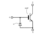
図20は、図18の半導体装置を示す等価回路図である。保護用ダイオード81を構成する3個の単方向ダイオード81aが直列に接続されている。3個の単方向ダイオード81aのうち、上段の単方向ダイオード81aのカソードは制御回路91と接続するゲート端子Gに接続され、下段の単方向ダイオード81aのアノードはIGBT92のエミッタに接続されている。つまり、上段の単方向ダイオード81aは、保護用ダイオード81の第1ダイオードであり、下段の単方向ダイオード81aは、保護用ダイオード81の第3ダイオードである。
FIG. 20 is an equivalent circuit diagram showing the semiconductor device of FIG. Three
図18〜20に示すように半導体装置800では、半導体(低濃度n半導体層3)表面に絶縁膜60(LOCOS酸化膜)を介してポリシリコン層からなる保護用ダイオード81が形成され、この保護用ダイオード81のnカソード層22は、制御回路91を介してIGBT92のゲート電極10に接続される。そして、保護用ダイオード81のpアノード層21は、IGBT92のエミッタ電極12を介してnエミッタ層5に接続される。ゲート端子Gにサージ電圧が印加されると、保護用ダイオード81がブレークダウンしてサージ電圧をクランプし、IGBT92のゲート電極10に高電圧が印加されない。その結果、IGBT92はサージ電圧から保護される。
As shown in FIGS. 18 to 20, in the
また、半導体装置800では、単方向ダイオード81aを3個直列に接続することで保護用ダイオード81として必要な耐圧を得ている。例えば、車載用途では通常の動作時のゲート入力電圧は5Vであるが、取り扱いの際に12Vのバッテリー電圧が誤ってゲート端子に印加されることがある。このような誤入力から保護用ダイオード81自身を保護するためにバッテリー電圧以上の耐圧が必要である。かつ、IGBT92のゲート保護のためにはIGBT92のゲートに印加される電圧をゲート耐圧以下にする必要がある。保護用ダイオード81の耐圧は単方向ダイオード81aの個数を変更することで調整することができる。しかしながら、単方向ダイオード81aの個数が増えると、保護用ダイオード81が形成される領域(保護用ダイオード領域)の面積が大きくなる。つまり、半導体装置800のチップ面積が大きくなる。
Further, in the
そこで、保護用ダイオード81の面積を縮小化する方法について説明する。図21は、従来の保護用ダイオードの別の一例の要部を示す平面図である。図21には、図18,19に比べて面積の縮小化を実現した保護用ダイオード82を示す。保護用ダイオード82は、pアノード層21とnカソード層22とが交互に複数配置されたポリシリコン層からなる多段の単方向ダイオード81aで構成される。隣り合う単方向ダイオード81aどうしは接続されている。つまり、多段の単方向ダイオード81aで構成された保護用ダイオード82は、単方向ダイオード81aのpアノード層21とnカソード層22とを交互に配置し、隣り合うpアノード層21とnカソード層22とを接続して、双方向に耐圧を有する双方向ダイオードを複数直列に接続した構成となっている。
Therefore, a method for reducing the area of the
図22は、従来の保護用ダイオードと制御回路との接続関係を示す結線図である。保護用ダイオード82は、ゲート端子GとIGBT92のエミッタ電極12(エミッタ端子E)との間に挿入され、順逆方向とも双方向ダイオードがブレークダウンするまでは電流は立ち上がらない。
FIG. 22 is a connection diagram illustrating a connection relationship between a conventional protection diode and a control circuit. The
つぎに、保護用ダイオード83をIGBTのコレクタとゲート間に挿入してサージ電圧から半導体装置を保護する例について説明する。図23は、従来の保護用ダイオードを有する半導体装置の別の一例の要部を示す説明図である。図23は、双方向ダイオードからなる保護用ダイオード83を搭載した半導体装置の構成を示す説明図である。図23(a)は、図23に示す半導体装置の全体の平面レイアウト図である。図23(b)は、図23に示す半導体装置の要部を示す断面図である。図23(c)は、保護用ダイオード83の要部を示す平面図である。図24は、図23の半導体装置を示す等価回路図である。図23に示すように半導体装置900において、保護用ダイオード83のカソード電極51はIGBT92のストッパ層85、コレクタ層となるp半導体基板1およびコレクタ電極11を経由してコレクタ端子Cと接続される。保護用ダイオード83のアノード電極52はIGBT92のゲート電極10に接続される。ストッパ層85はコレクタ層と同電位である。
Next, an example in which a
図23(b)に示すように、半導体装置900では、例えばIGBT領域が制御回路領域と保護用ダイオード領域の間に設けられている。制御回路91およびIGBT92の構成は、図18と同様である。
As shown in FIG. 23B, in the
コレクタ端子Cに外来のサージ電圧やIGBT92のスイッチング時のターンオフ電圧などの高電圧が印加されると、保護用ダイオード83がIGBT92より先にブレークダウンする。このブレークダウンによりIGBT92のコレクタから保護用ダイオード83を経由して制御回路91内の抵抗Rg(図22参照)に電流が流れて抵抗Rgに電圧が発生する。この電圧がIGBT92のゲートに印加されてIGBT92のゲート電位が上昇し、ゲート電位がゲートしきい値電圧以上になるとIGBT92がオン動作する。このオン動作によりIGBT92のコレクタには一定以上の高電圧が印加されない。
When a high voltage such as an external surge voltage or a turn-off voltage when switching the
また、保護用ダイオード83は、図21に示す保護用ダイオード82と同様に、絶縁膜60上に形成されたポリシリコン層からなる双方向ダイオードで構成される。この双方向ダイオードのpアノード層21とnカソード層23とも高不純物濃度であり、双方向ダイオードは双方向ツェナーダイオードとなる。保護用ダイオード83は、例えば気相拡散で形成される。
The
また、例えば下記特許文献1には、双方向ツェナーダイオードで保護用ダイオードを形成した半導体装置について提案されている。下記特許文献1では、双方向ツェナーダイオードは、高不純物濃度のpアノード層と、このpアノード層より低い不純物濃度のnカソード層とで構成されている。
For example,
前記した内容をまとめると、次のようになる。
(1)保護用ダイオード81,83の耐圧や高い破壊耐量を確保するためには、保護用ダイオード81,83を構成する単体の単方向ダイオード81aの接合面積を大きくして、単方向ダイオード81aの個数を増やす必要がある。しかしながら、保護用ダイオード81,83の面積が大きくなり、チップ面積が大きくなってしまう。
(2)pアノード層21およびnカソード層22,23の不純物濃度が高いと単体の単方向ダイオード81aの耐圧は低くなる。保護用ダイオード81,83として必要な耐圧を確保するためには、単方向ダイオード81aの個数を増やす必要がある。しかしながら、単方向ダイオード81aの個数を増やすと保護用ダイオード81,83の面積が大きくなり、チップ面積が大きくなってしまう。さらに、pアノード層21およびnカソード層22,23を気相拡散によって形成する場合、pアノード層21およびnカソード層22,23の面積は大きくなり、保護用ダイオード81、83の面積が増大するため、チップ面積が大きくなってしまう。
(3)単体の単方向ダイオード81aのpアノード層21またはnカソード層22,23の不純物濃度を低くして耐圧を高くし、かつ単方向ダイオード81aの個数を減らして所望の保護用ダイオード81,83の耐圧を確保しようとすると、図12に示すように、クランプ電圧が繰り返し印加されたときに保護用ダイオード81、83の耐圧が上昇して、保護用ダイオード81,83としての保護機能が失われる。
(4)保護用ダイオードの面積を縮小化するために、双方向ダイオードで構成した保護用ダイオード83とすると、ゲート端子Gに負のサージ電圧が印加された際に制御回路91を構成するMOSFETのボディーダイオード(寄生ダイオード)が順方向にバイアスされ、ゲート端子Gに向って大きな電流が流れてMOSFETが破壊する。そのため、ゲート端子Gに双方向ダイオードで構成された保護用ダイオード83のカソードを接続した場合には、半導体装置を負のサージ電圧から保護できない。The above contents are summarized as follows.
(1) In order to ensure the breakdown voltage and high breakdown resistance of the
(2) When the impurity concentrations of the
(3) The impurity concentration of the
(4) In order to reduce the area of the protective diode, if the
また、上記特許文献1には、pn接合を一つおきに金属膜で短絡して双方向ダイオードを単方向ダイオードにした保護用ダイオードについては記載されていない。また、p高濃度層/p低濃度層/n中濃度層/n高濃度層の4層構造については記載されていない。さらに繰り返しのクランプ電圧による保護用ダイオードの耐圧上昇を防止する方策については記載されていない。低濃度層は、保護用ダイオードを構成する複数の単方向ダイオードのうち、他の単方向ダイオードよりも低い不純物濃度を有する。中濃度層は、低濃度層よりも高く、かつ高濃度層よりも低い不純物濃度を有する。
Further,
この発明は、上述した従来技術による問題点を解消するため、高い破壊耐量とチップ面積の縮小化とを両立した半導体装置を提供することを目的とする。また、クランプ電圧が繰り返し印加されても耐圧の上昇を抑制することができる半導体装置を提供することを目的とする。また、ゲート端子に入力される負のサージ電圧による破壊を防止することができる半導体装置を提供することを目的とする。 SUMMARY OF THE INVENTION An object of the present invention is to provide a semiconductor device that achieves both a high breakdown tolerance and a reduction in chip area in order to solve the above-described problems caused by the prior art. Another object of the present invention is to provide a semiconductor device that can suppress an increase in breakdown voltage even when a clamp voltage is repeatedly applied. It is another object of the present invention to provide a semiconductor device capable of preventing destruction due to a negative surge voltage input to a gate terminal.
上述した課題を解決し、本発明の目的を達成するため、この発明にかかる半導体装置は、少なくとも半導体素子と、当該半導体素子が形成された半導体基板上に絶縁膜を介して形成された保護用ダイオードとを有する半導体装置において、前記保護用ダイオードが、n型半導体層とp型半導体層とが交互に複数接して配置され、かつ当該n型半導体層と当該p型半導体層とからなるpn接合が一つおきに導電膜で短絡された複数の単方向ダイオードで構成され、前記保護用ダイオードのカソード電極が前記半導体素子のゲート電極と接続し、前記保護用ダイオードのアノード電極が前記半導体素子の低電位側主電極(IGBTの場合はエミッタ電極、nチャネルMOSFETの場合はソース電極)と接続することを特徴とする。 To solve the above problems and achieve an object of the present invention, a semiconductor device according to this invention, which is formed through at least a semiconductor element, an insulating film on a semiconductor substrate in which the semiconductor element is formed protected In the semiconductor device having the diode for protection, the protective diode is a pn formed by alternately arranging a plurality of n-type semiconductor layers and p-type semiconductor layers, and comprising the n-type semiconductor layer and the p-type semiconductor layer. Every other junction is composed of a plurality of unidirectional diodes that are short-circuited with a conductive film, the cathode electrode of the protective diode is connected to the gate electrode of the semiconductor element, and the anode electrode of the protective diode is the semiconductor element And a low potential side main electrode (emitter electrode in the case of IGBT, source electrode in the case of n-channel MOSFET).
また、上述した従来技術による問題点を解消するため、この発明にかかる半導体装置は、少なくとも半導体素子と、当該半導体素子が形成された半導体基板上に絶縁膜を介して形成された保護用ダイオードとを有する半導体装置において、前記保護用ダイオードが、n型半導体層とp型半導体層とが交互に複数接して配置され、かつ当該n型半導体層と当該p型半導体層とからなるpn接合が一つおきに導電膜で短絡された複数の単方向ダイオードで構成され、前記保護用ダイオードのカソード電極が前記半導体素子の高電位側主電極(IGBTの場合はコレクタ電極、nチャネルMOSFETの場合はドレイン電極)と接続し、前記保護用ダイオードのアノード電極が前記半導体素子のゲート電極と接続することを特徴とする。ここで、一つおきに短絡されるpn接合は、順バイアス時に逆阻止状態となる接合である。 In order to solve the above-described problems due to the prior art, a semiconductor device according to the present invention includes at least a semiconductor element, and a protective diode formed on a semiconductor substrate on which the semiconductor element is formed via an insulating film. In the semiconductor device having the above structure, the protective diode is arranged such that a plurality of n-type semiconductor layers and p-type semiconductor layers are alternately in contact with each other, and a single pn junction composed of the n-type semiconductor layer and the p-type semiconductor layer is provided. It is composed of a plurality of unidirectional diodes that are short-circuited by conductive films, and the cathode electrode of the protective diode is the high potential side main electrode of the semiconductor element (collector electrode in the case of IGBT, drain in the case of n-channel MOSFET) And an anode electrode of the protective diode is connected to a gate electrode of the semiconductor element. Here, every other pn junction that is short-circuited is a junction that is in a reverse blocking state during forward bias.
また、この発明かかる半導体装置は、上述した発明において、前記保護用ダイオードのカソード電極またはアノード電極が、前記半導体基板に形成された制御回路を介して前記半導体素子のゲート電極に接続することを特徴とする。 In the invention such a semiconductor device of this, in the invention described above, that the cathode electrode or the anode electrode of the protective diode is connected to the gate electrode of the semiconductor element via a control circuit formed on the semiconductor substrate Features.
また、この発明にかかる半導体装置は、上述した発明において、前記n型半導体層の不純物濃度が前記p型半導体層の不純物濃度より低く、前記n型半導体層の不純物ドーズ量が1×1013cm-2以上5×1014cm-2以下であることを特徴とする。 Further, the semiconductor device according to this invention, in the invention described above, the impurity concentration of the n-type semiconductor layer is lower than the impurity concentration of the p-type semiconductor layer, the impurity dose amount of the n-type semiconductor layer is 1 × 10 13 It is characterized by being not less than cm −2 and not more than 5 × 10 14 cm −2 .
また、この発明にかかる半導体装置は、上述した発明において、前記保護用ダイオードの前記pn接合と前記n型半導体層上の前記導電膜の間の距離が1.5μm以上4.0μm以下であることを特徴とする。 The semiconductor device according to this invention is the invention described above, the distance between the conductive film on the n-type semiconductor layer and the pn junction of the protection diode is 1.5μm or more 4.0μm or less It is characterized by that.
また、この発明にかかる半導体装置は、上述した発明において、前記保護用ダイオードのカソード電極と接する前記n型半導体層が低濃度層と高濃度層で形成され、前記低濃度層の不純物ドーズ量が1×1013cm-2以上5×1014cm-2以下であり、前記高濃度層の不純物ドーズ量が当該低濃度層の不純物ドーズ量よりも高いことを特徴とする。 The semiconductor device according to this invention is the invention described above, the n-type semiconductor layer in contact with the cathode electrode of the protection diode is formed at a low concentration layer and the high concentration layer, the impurity dose amount of the low concentration layer Is not less than 1 × 10 13 cm −2 and not more than 5 × 10 14 cm −2 , and the impurity dose of the high concentration layer is higher than the impurity dose of the low concentration layer.
また、この発明にかかる半導体装置は、上述した発明において、前記保護用ダイオードのカソード電極および当該カソード電極と接する前記n型半導体層がそれぞれ複数形成されることを特徴とする。 The semiconductor device according to this invention is the invention described above, the n-type semiconductor layer in contact with the cathode electrode and the cathode electrode of the protection diode is characterized in that a plurality of formed respectively.
また、この発明にかかる半導体装置は、上述した発明において、前記導電膜で短絡したpn接合の平面形状は、前記n型半導体層と前記p型半導体層とが凹凸状に入り組んだ形状となっていることを特徴とする。 The semiconductor device according to this invention is the invention described above, the planar shape of the pn junction shorted by the conductive film, a the n-type semiconductor layer and the p-type semiconductor layer is an intricate shape uneven It is characterized by.
また、上述した従来技術による問題点を解消するため、この発明にかかる半導体装置は、少なくとも半導体素子と、当該半導体素子が形成された半導体基板上に絶縁膜を介して形成された保護用ダイオードとを有する半導体装置において、前記保護用ダイオードのカソード電極が前記半導体素子のゲート電極と接続し、前記保護用ダイオードのアノード電極が前記半導体素子の低電位側主電極と接続し、前記保護用ダイオードが、高濃度の第1導電型半導体層、中濃度の第1導電型半導体層、低濃度の第2導電型半導体層、高濃度の第2導電型半導体層の順に接して形成した4層の単方向ダイオードからなり、前記低濃度の第2導電型半導体層の幅が、クランプ電圧で空乏層がリーチスルーする幅であることを特徴とする。ここで、保護用ダイオードを構成する複数の半導体層のうち、他の半導体層よりも不純物濃度が低い場合を低濃度とし、低濃度の半導体層よりも不純物濃度が高い場合を中濃度および高濃度とする。中濃度の半導体層は、高濃度の半導体層よりも不純物濃度が低い(以下、他の請求項についても同様)。 Further, in order to solve the problems in the conventional techniques described above, the semiconductor device according to this invention, at least a semiconductor element, a protective diode to the semiconductor element is formed on a semiconductor substrate formed with an insulating film A cathode electrode of the protection diode is connected to a gate electrode of the semiconductor element, an anode electrode of the protection diode is connected to a low-potential side main electrode of the semiconductor element, and the protection diode Are formed in contact with a high-concentration first conductive semiconductor layer, a medium-concentration first conductive semiconductor layer, a low-concentration second conductive semiconductor layer, and a high-concentration second conductive semiconductor layer in this order. It is composed of a unidirectional diode, and the width of the low-concentration second conductive semiconductor layer is a width that allows the depletion layer to reach through with a clamp voltage. Here, among the plurality of semiconductor layers constituting the protective diode, the case where the impurity concentration is lower than the other semiconductor layers is set to low concentration, and the case where the impurity concentration is higher than the low concentration semiconductor layer is set to medium concentration and high concentration And The medium concentration semiconductor layer has a lower impurity concentration than the high concentration semiconductor layer (hereinafter the same applies to other claims).
また、上述した従来技術による問題点を解消するため、この発明にかかる半導体装置は、少なくとも半導体素子と、当該半導体素子が形成された半導体基板上に絶縁膜を介して形成された保護用ダイオードとを有する半導体装置において、前記保護用ダイオードのカソード電極が前記半導体素子の高電位側主電極に接続し、前記保護用ダイオードのアノード電極が前記半導体素子のゲート電極に接続し、前記保護用ダイオードが、高濃度の第1導電型半導体層、中濃度の第1導電型半導体層、低濃度の第2導電型半導体層、高濃度の第2導電型半導体層の順に接して形成した4層の単方向ダイオードからなり、前記低濃度の第2導電型半導体層の幅が、クランプ電圧で空乏層がリーチスルーを起こす幅であることを特徴とする。 Further, in order to solve the problems in the conventional techniques described above, the semiconductor device according to this invention, at least a semiconductor element, a protective diode to the semiconductor element is formed on a semiconductor substrate formed with an insulating film A cathode electrode of the protection diode is connected to a high potential side main electrode of the semiconductor element, an anode electrode of the protection diode is connected to a gate electrode of the semiconductor element, and the protection diode Are formed in contact with a high-concentration first conductive semiconductor layer, a medium-concentration first conductive semiconductor layer, a low-concentration second conductive semiconductor layer, and a high-concentration second conductive semiconductor layer in this order. It is composed of a unidirectional diode, and the width of the low-concentration second conductivity type semiconductor layer is a width that causes the depletion layer to reach through with a clamp voltage.
また、この発明にかかる半導体装置は、上述した発明において、前記保護用ダイオードのカソード電極またはアノード電極が、前記半導体基板に形成された制御回路を介して前記半導体素子のゲート電極に接続することを特徴とする。 The semiconductor device according to this invention is the invention described above, the cathode electrode or the anode electrode of the protective diode is connected to the gate electrode of the semiconductor element via a control circuit formed on the semiconductor substrate It is characterized by.
また、この発明にかかる半導体装置は、上述した発明において、前記保護用ダイオードが、前記4層の単方向ダイオードを順方向に直列接続して形成した多段の単方向ダイオードであることを特徴とする。 The semiconductor device according to this invention, and characterized in that in the invention described above, the protective diode is a multi-stage unidirectional diodes unidirectional diode formed by serially connected in a forward direction of the four-layer To do.
また、上述した従来技術による問題点を解消するため、この発明にかかる半導体装置は、少なくとも半導体素子と、当該半導体素子が形成された半導体基板上に絶縁膜を介して形成された保護用ダイオードとを有する半導体装置において、前記保護用ダイオードの一方の主電極が前記半導体素子の低電位側主電極に接続し、前記保護用ダイオードの他方の主電極が前記半導体素子のゲート電極に接続し、前記保護用ダイオードが、高濃度の第1導電型半導体層、中濃度の第1導電型半導体層、低濃度の第2導電型半導体層、高濃度の第2導電型半導体層、低濃度の第2導電型半導体層、中濃度の第1導電型半導体層、高濃度の第1導電型半導体層の順に接して形成された7層の双方向ダイオードからなり、前記低濃度の第2導電型半導体層の幅が、クランプ電圧で空乏層がリーチスルーを起こす幅であることを特徴とする。 Further, in order to solve the problems in the conventional techniques described above, the semiconductor device according to this invention, at least a semiconductor element, a protective diode to the semiconductor element is formed on a semiconductor substrate formed with an insulating film And one main electrode of the protective diode is connected to the low-potential side main electrode of the semiconductor element, and the other main electrode of the protective diode is connected to the gate electrode of the semiconductor element, The protective diode includes a high-concentration first conductive semiconductor layer, a medium-concentration first conductive semiconductor layer, a low-concentration second conductive semiconductor layer, a high-concentration second conductive semiconductor layer, and a low-concentration second conductive semiconductor layer. The low-concentration second conductive semiconductor is composed of a two-conductivity semiconductor layer, a seven-layer bidirectional diode formed in contact with the first-concentration first-conductivity-type semiconductor layer, and the high-concentration first-conductivity-type semiconductor layer. Layered But wherein the depletion layer in the clamp voltage is wide to cause a reach-through.
また、上述した従来技術による問題点を解消するため、この発明にかかる半導体装置は、少なくとも半導体素子と、当該半導体素子が形成された半導体基板上に絶縁膜を介して形成された保護用ダイオードとを有する半導体装置において、前記保護用ダイオードの一方の主電極が前記半導体素子の高電位側主電極に接続し、前記保護用ダイオードの他方の主電極が前記半導体素子のゲート電極に接続し、前記保護用ダイオードが、高濃度の第1導電型半導体層、中濃度の第1導電型半導体層、低濃度の第2導電型半導体層、高濃度の第2導電型半導体層、低濃度の第2導電型半導体層、中濃度の第1導電型半導体層、高濃度の第1導電型半導体層の順に接して形成した7層の双方向ダイオードからなり、前記低濃度の第2導電型半導体層の幅が、クランプ電圧で空乏層がリーチスルーを起こす幅であることを特徴とする。 Further, in order to solve the problems in the conventional techniques described above, the semiconductor device according to this invention, at least a semiconductor element, a protective diode to the semiconductor element is formed on a semiconductor substrate formed with an insulating film And one main electrode of the protective diode is connected to the high potential side main electrode of the semiconductor element, the other main electrode of the protective diode is connected to the gate electrode of the semiconductor element, The protective diode includes a high-concentration first conductive semiconductor layer, a medium-concentration first conductive semiconductor layer, a low-concentration second conductive semiconductor layer, a high-concentration second conductive semiconductor layer, and a low-concentration second conductive semiconductor layer. The low-concentration second conductive semiconductor layer is composed of a seven-layer bidirectional diode formed by contacting a two-conductivity type semiconductor layer, a medium-concentration first conductive-type semiconductor layer, and a high-concentration first conductive-type semiconductor layer in this order. Width of , Wherein the depletion layer in the clamp voltage is wide to cause a reach-through.
また、この発明にかかる半導体装置は、上述した発明において、前記保護用ダイオードの他方の主電極が、前記半導体基板に形成された制御回路を介して前記半導体素子のゲート電極に接続することを特徴とする。 Further, the semiconductor device according to this invention, in the invention described above, that the other main electrode of the protective diode, connected to the gate electrode of the semiconductor element via a control circuit formed on the semiconductor substrate Features.
また、この発明にかかる半導体装置は、上述した発明において、前記保護用ダイオードが、前記7層の双方向ダイオードを直列接続して形成された多段の双方向ダイオードからなることを特徴とする。 Further, the semiconductor device according to this invention, in the invention described above, the protective diode, characterized in that it consists of the 7-layer multi-stage bidirectional diodes bidirectional diode formed by series connection of.
また、この発明にかかる半導体装置は、上述した発明において、前記7層の双方向ダイオードの直列接続した箇所の主電極を除去することを特徴とする。 The semiconductor device according to this invention is the invention described above, and removing the main electrode portions connected in series of bidirectional diodes of the seven layers.
また、この発明にかかる半導体装置は、上述した発明において、前記保護用ダイオードがポリシリコン層または単結晶シリコン層からなることを特徴とする。 The semiconductor device according to this invention is the invention described above, wherein the protective diode is a polysilicon layer or a single crystal silicon layer.
また、この発明にかかる半導体装置は、上述した発明において、前記保護用ダイオードの前記低濃度の第2導電型半導体層が低濃度のp型半導体層からなるとき、当該低濃度のp型半導体層の幅が2μm以下であることを特徴とする。 The semiconductor device according to this invention is the invention described above, when the low concentration second conductivity type semiconductor layer of said protective diode is formed of a low concentration p-type semiconductor layer, p-type of this low concentration The width of the semiconductor layer is 2 μm or less.
また、この発明にかかる半導体装置は、上述した発明において、前記半導体素子が、パワーMOS型素子であるIGBT(絶縁ゲート型バイポーラトランジスタ)もしくはMOSFET(MOS駆動型電界効果トランジスタ)であることを特徴とする。 Further, characterized in that the semiconductor device according to this invention, in the invention described above, the semiconductor device is an IGBT is a power MOS type element (insulated gate bipolar transistor) or MOSFET (MOS driver field effect transistors) And
上述した発明によれば、pアノード層とnカソード層を交互に形成し、順バイアス時に逆阻止状態になるpn接合を一つおきに導電膜(金属膜)で短絡する保護用ダイオードを半導体素子に接続することで、サージ電圧に対して高い破壊耐量を有し、かつチップ面積の小さな半導体装置を提供することができる。また、半導体装置のゲート端子に入力される負のサージ電圧に対して高い破壊耐量を確保することできる。 According to the above-described invention, the protective diode in which the p anode layer and the n cathode layer are alternately formed and the pn junction that is reversely blocked in the forward bias state is short-circuited by the conductive film (metal film) is provided in the semiconductor element. By connecting to the semiconductor device, it is possible to provide a semiconductor device having a high breakdown resistance against a surge voltage and a small chip area. In addition, a high breakdown resistance can be ensured against a negative surge voltage input to the gate terminal of the semiconductor device.
また、pアノード層の不純物濃度よりnカソード層の不純物濃度を低くし、このnカソード層の不純物濃度をドーズ量1×1013cm-2以上5×1014cm-2以下とすることで、繰り返しクランプ電圧が印加された場合でも保護用ダイオードの耐圧が上昇することを抑制することができる。Further, the impurity concentration of the n cathode layer is made lower than the impurity concentration of the p anode layer, and the impurity concentration of the n cathode layer is set to a dose of 1 × 10 13 cm −2 or more and 5 × 10 14 cm −2 or less, Even when the clamp voltage is repeatedly applied, it is possible to suppress an increase in the breakdown voltage of the protective diode.
また、nカソード層の幅を1.5μm以上にすることで、繰り返しクランプ電圧が印加された場合でも保護用ダイオードの耐圧が上昇することを抑制することができる。また、nカソード層の幅を4.0μm以下とすることで、動作抵抗を低く抑えることができる。 Further, by setting the width of the n cathode layer to 1.5 μm or more, it is possible to suppress an increase in the breakdown voltage of the protective diode even when a clamp voltage is repeatedly applied. Further, when the width of the n cathode layer is 4.0 μm or less, the operating resistance can be suppressed low.
また、保護用ダイオードのカソード電極と接するnカソード層を低濃度層と高濃度層で形成し、高濃度層を低濃度の不純物ドーズである1×1013cm-2以上5×1014cm-2以下より高くすることでオーミックコンタクトが得られる。また、このカソード電極とnカソード層を複数接して形成し、複数のカソード電極の中からカソード電極を選択することで保護用ダイオードの耐圧を変更および調整することができる。Further, an n cathode layer in contact with the cathode electrode of the protective diode is formed of a low concentration layer and a high concentration layer, and the high concentration layer is a low concentration impurity dose of 1 × 10 13 cm −2 or more and 5 × 10 14 cm −. An ohmic contact can be obtained by making it higher than 2 or less. Also, the breakdown voltage of the protective diode can be changed and adjusted by forming a plurality of cathode electrodes and n cathode layers in contact with each other and selecting a cathode electrode from the plurality of cathode electrodes.
また、nカソード層の不純物濃度よりpアノード層の不純物濃度を低くし、pアノード層の幅をクランプ電圧が印加された場合に空乏層が伸びる長さより狭くして、空乏層がリーチスルーする状態とすることで、繰り返しクランプ電圧が印加された場合でも保護用ダイオードを一定の電圧に保つことができる。 Also, the impurity concentration of the p anode layer is made lower than the impurity concentration of the n cathode layer, and the width of the p anode layer is made narrower than the length of the depletion layer when a clamp voltage is applied, so that the depletion layer reaches through. Thus, even when a clamp voltage is repeatedly applied, the protective diode can be kept at a constant voltage.
また、nカソード層を、pアノード層(低濃度の第2導電型半導体層)より不純物濃度が高い第1n層(中濃度の第1導電型半導体層)とこの第1n層よりさらに高い第2n層(高濃度の第1導電型半導体層)とで構成し、pアノード層の幅を2μm以下にすることで、pアノード層の不純物濃度が低い場合には、繰り返しクランプ電圧が印加された場合に空乏層がリーチスルーして保護用ダイオードの耐圧は一定となる。一方、pアノード層の不純物濃度がリーチスルーしない高い不純物濃度の場合には、そもそも繰り返しクランプ電圧が印加された場合に保護用ダイオードの耐圧は上昇しない。つまり、pアノード層の幅を2μm以下とすれば、繰り返しクランプ電圧が印加された場合に、保護用ダイオードの耐圧の上昇を抑制することができる。さらに、第1n層を設けることで、第1n層を設けない場合に比べて、第1n層に広がる空乏層が伸びるため、高耐圧化を図ることができる。
Further, the n cathode layer is divided into a first n layer (medium concentration first conductivity type semiconductor layer) having a higher impurity concentration than the p anode layer (low concentration second conductivity type semiconductor layer) and a second n higher than this first n layer. When the impurity concentration of the p anode layer is low by making the width of the
本発明にかかる半導体装置によれば、高い破壊耐量とチップ面積の縮小化とを両立することができるという効果を奏する。また、クランプ電圧が繰り返し印加されても耐圧の上昇を抑制することができるという効果を奏する。また、ゲート端子に入力される負のサージ電圧による破壊を防止することができるという効果を奏する。 According to the semiconductor device of the present invention, there is an effect that it is possible to achieve both high breakdown tolerance and reduction in chip area. Moreover, even if the clamp voltage is repeatedly applied, an increase in breakdown voltage can be suppressed. In addition, there is an effect that the breakdown due to the negative surge voltage input to the gate terminal can be prevented.
以下に添付図面を参照して、この発明にかかる吸着機構の好適な実施の形態を詳細に説明する。なお、以下の実施の形態の説明および添付図面において、同様の構成には同一の符号を付し、重複する説明を省略する。以下の説明で、pは導電型がp型、nは導電型がn型であることを表す。また、従来構造と同一部位には同一の符号を付した。 Exemplary embodiments of a suction mechanism according to the present invention will be explained below in detail with reference to the accompanying drawings. Note that, in the following description of the embodiments and the accompanying drawings, the same reference numerals are given to the same components, and duplicate descriptions are omitted. In the following description, p represents that the conductivity type is p-type, and n represents that the conductivity type is n-type. Moreover, the same code | symbol was attached | subjected to the site | part same as a conventional structure.
(実施の形態1)
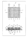
図1は、実施の形態1にかかる半導体装置の要部を示す説明図である。また、図2は、図1の保護用ダイオードの要部を示す平面図である。図2(a)は、保護用ダイオード71の要部を示す平面図である。図2(b)は、図2(a)の切断線A−A’における断面図である。また、図3は、図1の半導体装置を示す等価回路図である。また、図4は、図1の保護用ダイオードと制御回路との接続関係を示す結線図である。図1に示すように、半導体装置100は、低濃度n半導体層3の表面に、出力段となる縦型や横型のIGBT72が形成された領域(IGBT領域)と、IGBT72を駆動する横型MOSFETやダイオードおよび抵抗など複数のデバイスが形成されてそれぞれ所定の配線接続がなされた制御回路73が形成された領域(制御回路領域)と、保護用ダイオード71が形成された領域(保護用ダイオード領域)とで構成される。制御回路領域は、例えば、低濃度n半導体層3の中央部に配置される。IGBT領域は、制御回路領域に隣り合う(図1の紙面右側)。保護用ダイオード領域は、制御回路領域を挟んでIGBT領域と反対側に隣り合う(図1の紙面左側)。(Embodiment 1)
FIG. 1 is an explanatory diagram of a main part of the semiconductor device according to the first embodiment. FIG. 2 is a plan view showing a main part of the protective diode of FIG. FIG. 2A is a plan view showing a main part of the
図1に示す半導体装置100において、低濃度n半導体層3は、高濃度n半導体層2上に配置される。低濃度n半導体層3は、高濃度n半導体層2よりも低い不純物濃度を有する。高濃度n半導体層2は、p半導体基板1上に配置される。高濃度n半導体層2は、p半導体基板1よりも高い不純物濃度を有する。制御回路領域には、低濃度n半導体層3の表面層に複数のpウエル層34が配置される。pウエル層34は、互いに離れて複数配置される。各pウエル層34の表面層には、制御回路73を構成するMOSFET、ダイオードおよび抵抗Rg(不図示)などが配置される。図1に図示されたMOSFETおよびダイオードは、それぞれ異なるpウエル層34に配置される。具体的には、一方のpウエル層34の表面層には、MOSFETとしてnソース層35aおよびnドレイン層35bが設けられ、他方のpウエル層34の表面層には、ダイオードとしてnカソード層35cが設けられる。
In the
nソース層35aとnドレイン層35bとに挟まれたpウエル層34上には、ゲート絶縁膜37を介してゲート電極38が配置される。ソース電極54は、nソース層35aに接する。ドレイン電極55は、nドレイン層35bに接する。図示しないが、MOSFETが設けられたpウエル層34内には、ソース電極54と接続してMOSFETのボディダイオード(寄生ダイオード)が形成される。カソード電極56は、nカソード層35cに接する。アノード電極57は、nカソード層35cが設けられたpウエル層34に接する。
On the p-
IGBT領域には、低濃度n半導体層3の表面層にpウエル層4が配置される。pウエル層4の表面層には、パワー半導体素子であるIGBT72のnエミッタ層5が配置される。nエミッタ層5と低濃度n半導体層3とに挟まれたpウエル層4上には、ゲート絶縁膜7を介してゲート電極10が配置される。エミッタ電極12は、nエミッタ層5およびpウエル層4上に接する。また、pコレクタ層となるp半導体基板1の裏面にIGBT72を構成するコレクタ電極11が配置される。
In the IGBT region, a p-
保護用ダイオード領域には、低濃度n半導体層3上に絶縁膜60(LOCOS酸化膜)が形成されている。絶縁膜60上には、pアノード層21とnカソード層22が交互に配置されたポリシリコン層からなる保護用ダイオード71が配置される。つまり、保護用ダイオード71のpアノード層21とnカソード層22とでpn接合74が形成される。保護用ダイオード71のpアノード層21およびnカソード層22上には、層間絶縁膜61が設けられている。
In the protective diode region, an insulating film 60 (LOCOS oxide film) is formed on the low-concentration
図2に示すように、層間絶縁膜61には、コンタクトホール51a、コンタクトホール52aおよびコンタクトホール53aが形成されている。コンタクトホール51aは、制御回路領域から最も離れたnカソード層22を選択的に露出する。コンタクトホール52aは、制御回路領域に最も近いpアノード層21を選択的に露出する。コンタクトホール53aは、一つおきにpn接合74近傍のpアノード層21およびnカソード層22を選択的に露出する。
As shown in FIG. 2, a
コンタクトホール53aに露出するpアノード層21およびnカソード層22は金属膜(導電膜)53で短絡される。コンタクトホール51aに露出するnカソード層22はカソード電極51に接続する。コンタクトホール52aに露出するpアノード層21はアノード電極52に接続する。順バイアス時に逆阻止状態になるpn接合74を金属膜53で一つおきに短絡することで、保護用ダイオード71は直列接続した双方向ダイオードから直列接続した単方向ダイオード71aに変換される。
The
このように、ポリシリコン層からなる単方向ダイオード71aを複数接触させることで、単体の単方向ダイオード81aを直列接続する従来の保護用ダイオード81(図19参照)と比べて保護用ダイオード71の面積は小さくなる。その理由は、保護用ダイオード81のように単方向ダイオード81aを直列接続する場合、隣接する単方向ダイオード81aの間の隙間81b(図19参照)が生じるからである。これにより、保護用ダイオード71は、従来よりもチップ面積を縮小化することができる。
Thus, the area of the
また、図1に示すように、半導体装置100のゲート端子Gは、制御回路73を介してIGBT72のゲート電極10に接続される。保護用ダイオード71のカソード電極51は、半導体装置100のゲート端子Gにパッド電極58を介して接続される。さらに、保護用ダイオード71のカソード電極51は、制御回路73を介してIGBT72のゲート電極10に接続される。保護用ダイオード71のアノード電極52は、パッド電極59を介してIGBT72のエミッタ電極12に接続される。
As shown in FIG. 1, the gate terminal G of the
つまり、保護用ダイオード71は、ゲート端子GとIGBT72のエミッタ電極10の間に挿入される。これにより、制御回路73とIGBT72のゲートは保護用ダイオード71によってサージ電圧から保護される。保護用ダイオード71は、pアノード層21とnカソード層22の繰り返し数を変更することで、保護用ダイオード71の耐圧の変更および調整を行うことができる。
That is, the
また、保護用ダイオード71をIGBT72のサージ保護に用いることにより、高い破壊耐量とチップ面積の縮小化を図った半導体装置100を提供することができる。保護用ダイオード71を用いると、ゲート端子Gに負のサージが印加された場合にも、ボディダイオード(寄生ダイオード)に過大な電流が流れることがない。このため、制御回路73のMOSFETはサージから保護される。
Further, by using the
上述した説明では、保護用ダイオード71をIGBT72のゲートとエミッタに接続した場合について説明したが、保護用ダイオード71をIGBT72のゲートとコレクタに接続してもよい。この場合においても、サージからIGBT72を保護することができ、かつ高い破壊耐量を有する半導体装置100とすることができる。
In the above description, the case where the
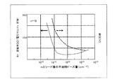
つぎに、保護用ダイオード71の耐圧安定性と諸元について説明する。図5〜7は、実施の形態1にかかる単方向ダイオードの電気的特性について示す特性図である。図5には、クランプ電圧印加による単方向ダイオード71aの耐圧変動率および初期の耐圧と、nカソード層22の不純物ドーズ量との関係を示す。図6には、耐圧と、pn接合74からnカソード層22上の金属膜53のpn接合74側の端部までの距離(以下、pn接合74と金属膜53の間の距離とする)L(図2参照)との関係を示す。図7には、保護用ダイオード71の動作抵抗とpn接合74と金属膜53の間の距離Lとの関係を示す図である。ここでいう耐圧は保護用ダイオード71のカソード−アノード間の耐圧であり、アバランシェ降伏またはリーチスルー降伏による耐圧である。また、保護用ダイオード71がクランプされる回数は耐圧がほぼ飽和する10回程度とした。
Next, breakdown voltage stability and specifications of the
図5に示すように、nカソード層22の不純物ドーズ量が低い程、耐圧は高くなる。このため、単方向ダイオード71aの直列数を減らしても所望の耐圧を維持することができ、保護用ダイオード71の面積を縮小化することができる。しかし、nカソード層22の不純物ドーズ量が低くなると、保護用ダイオード71にクランプ電圧が繰り返し印加された場合に保護用ダイオード71の耐圧は上昇してしまい、保護機能が低下する。一方、nカソード層22の不純物ドーズ量を高くすると、耐圧変動率は小さくなるが初期の耐圧が低下する。したがって、保護用ダイオード71の耐圧を確保するためには、単方向ダイオード71aの直列数を増加する必要があるが、保護用ダイオード71の面積は大きくなり、その結果、チップ面積が増大する。
As shown in FIG. 5, the lower the impurity dose of the
図6に示すように、pn接合74と金属膜53の間の距離Lが1.5μm以下になると、耐圧は低下する。その理由は、pn接合74から広がる空乏層が金属膜53に達してリーチスルーするからである。また、図7に示すように、pn接合74と金属膜53の間の距離Lが4.0μmより長くなると、動作抵抗は急激に大きくなる。
As shown in FIG. 6, when the distance L between the
したがって、保護用ダイオード71を次の(1)〜(3)のように形成すると、保護用ダイオード71の耐圧の上昇を抑制することができる。
(1)pアノード層21はnカソード層22よりも高い不純物濃度とし、nカソード層22はpアノード層21よりも低い不純物濃度とするのがよい。
(2)pアノード層21およびnカソード層22のそれぞれの領域の不純物ドーズ量は、pアノード層21が1.0×10¹⁵/cm2、nカソード層22が1.0×1013/cm2以上5.0×1014/cm2以下とするのがよい。
(3)pn接合74と金属膜53の間の距離Lを1.5μm以上4.0μm以下とするのがよい。Therefore, if the
(1) The
(2) The impurity doses in the respective regions of the
(3) The distance L between the
また、pアノード層21およびnカソード層22をイオン注入で形成することで、従来の気相拡散で各層を形成する場合に比べて各層の占有面積を小さくすることができる。
In addition, by forming the
以上、説明したように、実施の形態1によれば、ポリシリコン層からなるpアノード層21とnカソード層22を交互に形成し、順バイアス時に逆阻止状態になるpn接合を一つおきに金属膜53で短絡する保護用ダイオード71をIGBT72(パワー半導体素子)に接続することで、サージ電圧に対して高い破壊耐量を有し、かつチップ面積の小さな半導体装置100を提供することができる。また、半導体装置100のゲート端子Gに入力される負のサージ電圧に対して高い破壊耐量を確保することができる。
As described above, according to the first embodiment, the p anode layers 21 and the n cathode layers 22 made of the polysilicon layers are alternately formed, and every other pn junction that is in the reverse blocking state at the time of forward bias is formed. By connecting the
また、pアノード層21の不純物濃度よりnカソード層22の不純物濃度を低くし、nカソード層22の不純物濃度をドーズ量1×1013cm-2以上5×1014cm-2以下とすることで、繰り返しクランプ電圧が印加された場合でも保護用ダイオード71の耐圧が上昇することを抑制することができる。Further, the impurity concentration of the
また、nカソード層22の幅を1.5μm以上にすることで、繰り返しクランプ電圧が印加された場合でも保護用ダイオード71の耐圧が上昇することを抑制することができる。また、nカソード層22の幅を4.0μm以下とすることで、動作抵抗を低く抑えることができる。
In addition, by setting the width of the
(実施の形態2)
図8は、実施の形態2にかかる半導体装置の構成の要部を示す説明図である。図8(a)は、半導体装置200の要部を示す平面図である。図8(b)は、図8(a)の切断線A−A’における断面構造を示す断面図である。図8(c)は、図8(a)の切断線B−B’線における断面構造を示す断面図である。半導体装置200の断面構造は、実施の形態1の半導体装置100と同様である(図1参照)。図8には、半導体装置200を構成する保護用ダイオード75の構成のみを示す。(Embodiment 2)
FIG. 8 is an explanatory diagram of a main part of the configuration of the semiconductor device according to the second embodiment. FIG. 8A is a plan view showing the main part of the
実施の形態1の保護用ダイオード71と異なる点は、pアノード層21とnカソード層22のpn接合74がくし歯状に噛み合っている点である。つまり、金属膜53で短絡したpn接合74の平面形状は、pアノード層21とnカソード層22とが凹凸状に入り組んでいる。これにより、pアノード層21上とnカソード層22上に形成されるコンタクトホール53aの大きさを小さくしてもコンタクトに必要な面積を確保することができる。そのため、保護用ダイオード75の面積を小さくすることができる。その結果、実施の形態1と同様に高い破壊耐量とチップ面積の縮小化を図ることができる。
The difference from the
以上、説明したように、実施の形態2によれば、実施の形態1と同様の効果を得ることができる。 As described above, according to the second embodiment, the same effect as in the first embodiment can be obtained.
(実施の形態3)
図9は、実施の形態3にかかる半導体装置の要部を示す断面図である。実施の形態1と異なる点は、次の点である。半導体基板1に絶縁層16を介して半導体層が形成されたSOI(Silicon On Insulator)基板などを用いる。この半導体層を低濃度n半導体層3aとし、低濃度n半導体層3aの表面(SOI基板の表面)より絶縁層16に達する絶縁分離領域17を形成して低濃度n半導体層3aを分離する。そして、絶縁分離領域17によって分離した低濃度n半導体層3aのうちの1つに保護用ダイオード76を形成する点である。つまり、この半導体装置300を構成する保護用ダイオード76は、ポリシリコン層ではなく単結晶シリコン層(低濃度n半導体層3a)からなる。(Embodiment 3)
FIG. 9 is a cross-sectional view illustrating a main part of the semiconductor device according to the third embodiment. The difference from the first embodiment is as follows. An SOI (Silicon On Insulator) substrate in which a semiconductor layer is formed on the
また、IGBT72は低濃度n半導体層3aに形成された横型IGBTであり、pコレクタ層1aは低濃度n半導体層3aの表面層に形成されている。この場合においても実施の形態1と同様の高い破壊耐量を確保しつつチップ面積の縮小化を図ることができる。半導体基板の導電型はp型でもn型でも構わない。
The
以上、説明したように、実施の形態3によれば、実施の形態1と同様の効果を得ることができる。 As described above, according to the third embodiment, the same effect as in the first embodiment can be obtained.
(実施の形態4)
図10は、実施の形態4にかかる半導体装置の構成の要部を示す説明図である。図10(a)は、半導体装置400の要部を示す平面図である。図10(b)は、図10(a)の切断線A−A’における断面構造を示す断面図である。半導体装置400の断面構造は、実施の形態1の半導体装置100と同様である(図1参照)。図10には、半導体装置400を構成する保護用ダイオード77の構成のみを示す。(Embodiment 4)
FIG. 10 is an explanatory diagram of a main part of the configuration of the semiconductor device according to the fourth embodiment. FIG. 10A is a plan view showing the main part of the
実施の形態1の保護用ダイオード71と異なるのは、ゲート端子Gと接続する保護用ダイオード77のカソード電極51に接触する低濃度のnカソード層を、コンタクトホール30となる箇所近傍を高濃度のnカソード層23とし、それ以外の箇所を低濃度のnカソード層22とした、低濃度のnカソード層22と高濃度のnカソード層23との2層で形成した点である。低濃度のnカソード層22は、高濃度のnカソード層23よりも低い不純物濃度を有する。低濃度のnカソード層22にカソード電極51を形成する場合、コンタクト抵抗が大きくなることがあるため、コンタクト部分は高濃度であることが望ましい。また、IGBT72のエミッタ電極12に接続する保護用ダイオード77のアノード電極52は、コンタクトホール31を介して高濃度のnカソード層23に接する。
The difference from the
また、図2と異なるのはカソード電極51がアノード電極52より広くなっている点である。これによって、アノード電極52と接続する配線を狭くすることができる。また、カソード電極51を広くすることでpn接合74の断面積を大きくすることができるため、高い破壊耐量を確保することができる。
Also, the difference from FIG. 2 is that the
以上、説明したように、実施の形態4によれば、実施の形態1と同様の効果を得ることができる。また、半導体装置400は半導体装置100(図1参照)より多少チップ面積が増加するが、図18に示す従来の半導体装置800と比べると高い破壊耐量とチップ面積の縮小化を図ることができる。また、保護用ダイオード77のカソード電極51と接するnカソード層23を高濃度層として形成し、高濃度層を低濃度層(nカソード層22)の不純物ドーズである1×1013cm-2以上5×1014cm-2以下より高くすることでオーミックコンタクトが得られる。As described above, according to the fourth embodiment, the same effect as in the first embodiment can be obtained. Further, the
(実施の形態5)
図11は、実施の形態5にかかる半導体装置の構成の要部を示す説明図である。図11(a)は、半導体装置500の要部を示す平面図である。図11(b)は、図11(a)の切断線A−A’における断面構造を示す断面図である。半導体装置500の断面構造は、実施の形態1の半導体装置100と同様である(図1参照)。図11には、半導体装置500を構成する保護用ダイオード78の構成のみを示す。(Embodiment 5)
FIG. 11 is an explanatory diagram of a main part of the configuration of the semiconductor device according to the fifth embodiment. FIG. 11A is a plan view showing the main part of the
実施の形態1の保護用ダイオード71と異なるのは、独立した複数のカソード電極51を形成した点である。この場合、IGBT72のコレクタと接続する保護用ダイオード78のカソード電極51を複数のカソード電極51の中から選択することで、保護用ダイオード78の耐圧調整を行うことができる。
The difference from the
以上、説明したように、実施の形態5によれば、実施の形態1と同様の効果を得ることができる。また、半導体装置500は、半導体装置100より多少チップ面積が増加するが、図18に示す従来の半導体装置800と比べると高い破壊耐量とチップ面積の縮小化を図ることができる。
As described above, according to the fifth embodiment, the same effect as in the first embodiment can be obtained. Further, although the
上述した実施の形態1〜5では、低濃度のn半導体層(nカソード層)22の不純物濃度を所定の値に制御することで、クランプ電圧が複数回印加された場合でも保護用ダイオードの耐圧が上昇するのを防止できることを説明した。 In the first to fifth embodiments described above, by controlling the impurity concentration of the low-concentration n semiconductor layer (n cathode layer) 22 to a predetermined value, the withstand voltage of the protective diode is maintained even when a clamp voltage is applied multiple times. Explained that it can be prevented from rising.
つぎに、低濃度のn半導体層22の長さをクランプ電圧で確実に空乏層がリーチスルーする長さとすることで、クランプ電圧を繰り返し印加しても保護用ダイオードの耐圧上昇を抑制できる例について説明する。ここでは、実施の形態1の場合と不純物濃度が逆になっており、pアノード層が低濃度で、nカソード層が高濃度の場合を例に説明する。
Next, an example in which the length of the low-concentration
まず、クランプ回数の増加とともに保護用ダイオードの耐圧が上昇する様子を説明する。図12は、電圧クランプ回数と保護用ダイオードの耐圧の関係を示す説明図である。低濃度層であるp層の不純物濃度が1×1014cm-2、高濃度層であるn層の不純物濃度が5×1015cm-2および高濃度層であるp層の不純物濃度は3×1015cm-2である。図12に示すように、保護用ダイオードの耐圧はクランプ回数が増加するにつれて上昇し、クランプ回数が増えればカソード−アノード間耐圧は飽和傾向にある。この耐圧は、カソード−アノード間耐圧のことであり、アバランシェ降伏で起こる耐圧である。First, the manner in which the withstand voltage of the protective diode increases as the number of clamps increases will be described. FIG. 12 is an explanatory diagram showing the relationship between the number of voltage clamps and the withstand voltage of the protective diode. The impurity concentration of the p layer which is a low concentration layer is 1 × 10 14 cm −2 , the impurity concentration of the n layer which is a high concentration layer is 5 × 10 15 cm −2, and the impurity concentration of the p layer which is a high concentration layer is 3 × 10 15 cm -2 As shown in FIG. 12, the breakdown voltage of the protective diode increases as the number of clamps increases, and the cathode-anode breakdown voltage tends to be saturated as the number of clamps increases. This breakdown voltage is a breakdown voltage between the cathode and the anode, and is a breakdown voltage caused by avalanche breakdown.
(実施の形態6)
図13は、実施の形態6にかかる半導体装置の構成の要部を示す説明図である。図13(a)は、半導体装置600の要部を示す断面図である。図13(b)は、保護用ダイオード79を詳細に示す断面図である。半導体装置600を構成する保護用ダイオード79は単方向の単体ダイオードで構成されている。図14,15は、図13の半導体装置を示す等価回路図である。図14は、保護用ダイオード79をIGBTのゲート−エミッタ間に挿入した場合の等価回路図を示す。図15は、保護用ダイオード79をゲート−コレクタ間に挿入した場合の等価回路図を示す。保護用ダイオード79を構成する単方向ダイオードは、pアノード層41(低濃度層)、nカソード層42(中濃度層)、および両端に配置される高濃度のnカソード層43およびpアノード層40(高濃度層)である。pアノード層41は、nカソード層42よりも低い不純物濃度を有する。nカソード層42は、nカソード層43およびpアノード層40よりも低い不純物濃度を有する。nカソード層43は、nカソード層42に接する。nカソード層42は、pアノード層41に接する。pアノード層41は、pアノード層40に接する。nカソード層43およびpアノード層40は、それぞれカソード電極51とアノード電極52とのコンタクト層である。以下、保護用ダイオードを構成する複数の単方向ダイオードのうち、他の単方向ダイオードよりも不純物濃度が低い場合を低濃度とし、低濃度の層よりも不純物濃度が高い場合を中濃度および高濃度とする。中濃度の層は、高濃度の層よりも不純物濃度が低い。(Embodiment 6)
FIG. 13 is an explanatory diagram of a main part of the configuration of the semiconductor device according to the sixth embodiment. FIG. 13A is a cross-sectional view showing the main part of the
保護用ダイオード79である単方向ダイオードの製造方法について説明する。絶縁膜60(LOCOS酸化膜)上に厚さ0.5μmのポリシリコンを堆積し、フォトリソグラフィーとエッチングにより、ダイオードの形状に加工する。ポリシリコン層全面にボロンを例えばドーズ量6×1013cm-2以上9×1013cm-2以下程度と低濃度でイオン注入する。また、中濃度層であるnカソード層42に選択的にリンまたは砒素をドーズ量2×1014cm-2以上9×1014cm-2以下程度でイオン注入する。高濃度のpアノード層40には選択的にボロンを例えばドーズ量3×1015cm-2程度と高濃度でイオン注入する。高濃度のnカソード層43には選択的にリンまたは砒素を例えばドーズ量5×1015cm-2程度と高濃度でイオン注入する。このとき、高濃度のpアノード層40と中濃度のnカソード層42に挟まれた低濃度のpアノード層41の幅Mは2μm以下となるようにする。つまり、保護用ダイオード79は、n+層(高濃度のnカソード層43)/n層(中濃度のnカソード層42)/p-層(低濃度のアノード層41)/p+層(高濃度のpアノード層40)の4層の単方向ダイオードで構成される。保護用ダイオード79の端部に設けられるn+層とp+層は、金属配線とのオーミックコンタクトを得るために高濃度にする。A method of manufacturing the unidirectional diode that is the
保護用ダイオード79のpn接合48は、低濃度のpアノード層41と中濃度のnカソード層42によって形成される。低濃度のpアノード層41の幅Mがリーチスルーしない程度に大きい場合、カソード−アノード間に電圧が印加されたときに、pn接合48から伸びた空乏層が低濃度のpアノード層41へ広がっていきpn接合48での電界が臨界電界に達してアバランシェ降伏を起こす。このときの保護用ダイオード79の耐圧は、低濃度層と中濃度層の不純物濃度によって決まる。
The
また、低濃度のpアノード層41の幅Mがリーチスルーする程度に空乏層の広がり幅より小さい場合は、空乏層がリーチスルーする電圧で保護用ダイオード79の耐圧が決まる。つまり、保護用ダイオード79の耐圧は低濃度のpアノード層41の幅Mに依存する。
Further, when the width M of the low-concentration p anode layer 41 is smaller than the spread width of the depletion layer to reach through, the breakdown voltage of the
図16は、図13の保護用ダイオードの耐圧と低濃度のpアノード層の幅との関係を示す特性図である。保護用ダイオード79の耐圧とは、カソード−アノード間の耐圧である(以下、図17においても同様)。この例では、高濃度のpアノード層40、低濃度のpアノード層41、中濃度のnカソード層42はそれぞれ、ボロン3×1015cm-2、ボロン7×1013cm-2、砒素5×1014cm-2のイオン注入で形成されている。低濃度のpアノード層41の幅Mを短くしていくと、空乏層は高濃度のpアノード層40へリーチスルーするようになり、低濃度のpアノード層41の幅Mの縮小とともにカソード−アノード間耐圧は低下する。低濃度のpアノード層41の幅Mが0μmになると、カソード−アノード間耐圧は高濃度のpアノード層40と中濃度のnカソード層42のpn接合48で決まる耐圧となる。空乏層がリーチスルーを起こす幅は、中濃度のnカソード層42、および低濃度のpアノード層41をそれぞれ14乗台、13乗台のドーズ量のイオン注入で形成した場合、2μm程度であり、それ以下の幅ではリーチスルーが起こる。つまり、低濃度のpアノード層41の幅Mが2μm以下になるとカソード−アノード間耐圧はリーチスルーを起こす電圧で決まる。そのため、低濃度のpアノード層41の幅Mを2μm以下とすれば、繰り返しのクランプ電圧を印加しても保護用ダイオード79の耐圧の上昇は抑制される。また、中濃度のnカソード層42を低濃度のpアノード層41と同程度の不純物濃度にした場合には、保護用ダイオード79の耐圧を高めることができる。FIG. 16 is a characteristic diagram showing the relationship between the breakdown voltage of the protective diode of FIG. 13 and the width of the low-concentration p anode layer. The breakdown voltage of the
図17は、図13の保護用ダイオードの耐圧と電圧クランプ回数との関係を示す特性図である。図17では、低濃度のpアノード層41の幅Mをパラメータとしている。低濃度のpアノード層41の幅Mは、図16に示す幅X1,X2の値である。幅X1,X2の両方は同程度の初期の耐圧を示すが、M=X1で形成された単方向ダイオードはクランプ電圧ではリーチスルーを起こさない。一方、M=X2で形成された単方向ダイオードは、クランプ電圧でリーチスルーを起こす。リーチスルーを起こさない単方向ダイオード(M=X1)は、従来の単方向ダイオードと同様に、繰り返しのクランプ電圧を印加することで電圧は上昇する。 FIG. 17 is a characteristic diagram showing the relationship between the withstand voltage of the protective diode of FIG. 13 and the number of voltage clamps. In FIG. 17, the width M of the low-concentration p anode layer 41 is used as a parameter. The width M of the low-concentration p anode layer 41 is a value of the widths X1 and X2 shown in FIG. Although both widths X1 and X2 show the same initial breakdown voltage, the unidirectional diode formed with M = X1 does not reach through at the clamp voltage. On the other hand, the unidirectional diode formed with M = X2 causes reach through at the clamp voltage. In the unidirectional diode (M = X1) that does not cause reach-through, the voltage rises by applying a repetitive clamp voltage, as in the conventional unidirectional diode.
これに対し、リーチスルーを起こす単方向ダイオード(M=X2)は、耐圧の上昇は見られない。この保護用ダイオードは、上述したように、アノード端子が接する高濃度のpアノード層40と、カソード端子が接する高濃度のnカソード層43と、これらの高濃度層の間に両高濃度層よりも低濃度で形成された低濃度のpアノード層41と中濃度のnカソード層42が配置された複数の単方向ダイオードからなる(図13参照)。低濃度のpアノード層41の幅Mはクランプ電圧でリーチスルーを起こす幅(リーチスルー幅)に形成されているので、クランプ動作の繰り返しによる耐圧上昇を抑えた保護用ダイオードとなっている。また、中濃度のnカソード層42の不純物濃度と長さを変えることでカソード−アノード間耐圧を変えることが可能となる。
In contrast, the unidirectional diode (M = X2) that causes reach-through does not show an increase in breakdown voltage. As described above, the protective diode includes a high-concentration
保護用ダイオード79の低濃度のpアノード層41の幅Mを2μm以下とすることで、保護用ダイオード79の耐圧は空乏層がリーチスルーを起こす電圧(リーチスルー電圧)となり、繰り返しのクランプ電圧印加により保護用ダイオード79の耐圧が上昇することを防止できる。保護用ダイオード79の耐圧の上昇が抑制されることで、半導体装置600は高い破壊耐圧を有するようになる。さらに、クランプ電圧がリーチスルー電圧で決まることから、アバランシェ降伏電圧で決まる場合に比べて、低濃度のpアノード層41の幅Mを狭くすることができる。その結果、高い破壊耐量とチップ面積の縮小化を図ることができる。
By setting the width M of the low-concentration p anode layer 41 of the
実施の形態6では、図14のように、IGBT72のゲート−エミッタ間に単方向ダイオードを保護用ダイオード79として挿入する例を示したが、図15のようにコレクタ−ゲート間に挿入してもよい。
In the sixth embodiment, an example in which a unidirectional diode is inserted as a
また、図示しないが、実施の形態6の保護用ダイオード79において、低濃度のpアノード層41に代えて中濃度のpアノード層とし、中濃度のnカソード層42に代えて低濃度のnカソード層とし、この低濃度のnカソード層の幅をリーチスルーの生じる幅としても同様の効果を得ることができる。
Although not shown, in the
また、図示しないが、保護用ダイオードは、単方向ダイオードを順方向に直列接続して接続したアノード電極とカソード電極とを一つの金属膜で形成し、多段の単方向ダイオードとすることで、高耐圧化することができる。この場合、保護用ダイオードは、n+層(高濃度層)/n層(中濃度)/p-層(低濃度層)/p+層(高濃度層)/n+層(高濃度層)/n層(中濃度)/p-層(低濃度層)/p+層(高濃度層)/で構成される。そして、p+層(高濃度層)/n+層(高濃度層)の接合部上を一つの金属膜で被覆してオーミック接合にする。また、この構成を繰り返した構成とすることで、保護用ダイオードの耐圧を変更および調整することができる。Although not shown, the protective diode is formed by forming a multi-stage unidirectional diode by forming an anode electrode and a cathode electrode, which are unidirectional diodes connected in series in the forward direction, with a single metal film. The breakdown voltage can be increased. In this case, the protective diode is n + layer (high concentration layer) / n layer (medium concentration) / p − layer (low concentration layer) / p + layer (high concentration layer) / n + layer (high concentration layer). / N layer (medium concentration) / p − layer (low concentration layer) / p + layer (high concentration layer) /. Then, the p + layer (high concentration layer) / n + layer (high concentration layer) junction is covered with one metal film to form an ohmic junction. Further, by adopting a configuration in which this configuration is repeated, the withstand voltage of the protective diode can be changed and adjusted.
また、図示しないが、単方向ダイオードを背中合わせ(逆方向)に接続した双方向ダイオードで保護用ダイオードを構成しても構わない。この場合、保護用ダイオードは、n+層(高濃度層)/n層(中濃度)/p-層(低濃度層)/p+層(高濃度層)/p-層(低濃度層)/n層(中濃度層)/n+層(高濃度層)で構成される。また、この構成を繰り返した構成とすることで、保護用ダイオードの耐圧を変更および調整することができる。Although not shown, the protective diode may be formed of a bidirectional diode in which unidirectional diodes are connected back to back (reverse direction). In this case, the protective diode is n + layer (high concentration layer) / n layer (medium concentration) / p − layer (low concentration layer) / p + layer (high concentration layer) / p − layer (low concentration layer). / N layer (medium concentration layer) / n + layer (high concentration layer). Further, by adopting a configuration in which this configuration is repeated, the withstand voltage of the protective diode can be changed and adjusted.
また、上述したように、多数直列接続された双方向ダイオードのpn接合を一つおきに金属膜で短絡することで直列接続された単方向ダイオードとすることができる。この単方向ダイオードで構成される保護用ダイオードをIGBTのゲートとエミッタ間やゲートとコレクタ間に挿入しても同様の効果が得られる。 Further, as described above, a unidirectional diode connected in series can be obtained by short-circuiting every other pn junction of a plurality of serially connected bidirectional diodes with a metal film. The same effect can be obtained by inserting a protective diode composed of this unidirectional diode between the gate and emitter of the IGBT or between the gate and collector.
また、保護用ダイオード79はポリシリコン層に形成された例で説明したが、SOI基板など絶縁膜上に形成した単結晶シリコン層に形成しても構わない。これは実施の形態6で説明した保護用ダイオードすべてに適用することができる。
Further, although the
以上、説明したように、実施の形態6によれば、実施の形態1と同様の効果を得ることができる。 As described above, according to the sixth embodiment, the same effect as in the first embodiment can be obtained.
また、実施の形態1〜6では、被保護素子である半導体素子としてパワー半導体素子であるIGBT72を例に挙げて説明したが、パワーMOSFETなどのパワーMOS素子に本発明を適用することで前記と同様の効果を得ることができる。
In the first to sixth embodiments, the
以上のように、本発明にかかる半導体装置は、外来から印加されるサージ電圧やスイッチング時に素子自体から発生するサージ電圧からパワー半導体素子を保護するサージ保護用のダイオードをパワー半導体素子と同一半導体基板に形成した半導体装置に有用である。 As described above, the semiconductor device according to the present invention includes a surge protection diode that protects a power semiconductor element from a surge voltage applied from the outside or a surge voltage generated from the element itself during switching. It is useful for the semiconductor device formed in the above.
1 p半導体基板
1a pコレクタ層
2 高濃度n半導体層
3,3a 低濃度n半導体層
4 pウエル層
5 nエミッタ層
7 ゲート絶縁膜
10 ゲート電極
11 コレクタ電極
12 エミッタ電極
16 絶縁層(酸化膜)
17 絶縁分離領域
21,40 高濃度のpアノード層
22 低濃度のnカソード層
23,43 高濃度のnカソード層
30,31,51a,52a,53a コンタクトホール
34 pウエル層
35a nソース層
35b nドレイン層
35c nカソード層
37 ゲート絶縁膜
38 ゲート電極
41 低濃度のpアノード層
42 中濃度のnカソード層
48,74 pn接合
51,56 カソード電極
52,57 アノード電極
53 金属膜
54 ソース電極
55 ドレイン電極
58,59 パッド電極
60 絶縁膜
61 層間絶縁膜
71,75,76,77,78,79 保護用ダイオード
71a 単方向ダイオード
72 IGBT
73 制御回路
100,200,300,400,500,600,800,900 半導体装置
L pn接合と金属膜の間の距離
M 低濃度のpアノード層の幅
G ゲート端子
E エミッタ端子
C コレクタ端子DESCRIPTION OF SYMBOLS 1
17 Insulating
73
Claims (12)
前記保護用ダイオードのカソード電極が前記半導体素子のゲート電極と接続し、A cathode electrode of the protective diode is connected to a gate electrode of the semiconductor element;
前記保護用ダイオードのアノード電極が前記半導体素子の低電位側主電極と接続し、The anode electrode of the protective diode is connected to the low potential main electrode of the semiconductor element;
前記保護用ダイオードが、高濃度の第1導電型半導体層、中濃度の第1導電型半導体層、低濃度の第2導電型半導体層、高濃度の第2導電型半導体層の順に接して形成した4層の単方向ダイオードからなり、The protective diode is formed in contact with a high-concentration first conductive semiconductor layer, a medium-concentration first conductive semiconductor layer, a low-concentration second conductive semiconductor layer, and a high-concentration second conductive semiconductor layer in this order. 4 layers of unidirectional diodes,
前記低濃度の第2導電型半導体層の幅が、クランプ電圧で空乏層がリーチスルーする幅であることを特徴とする半導体装置。2. The semiconductor device according to claim 1, wherein a width of the low-concentration second conductive semiconductor layer is a width through which the depletion layer reaches through with a clamp voltage.
前記保護用ダイオードのカソード電極が前記半導体素子の高電位側主電極に接続し、A cathode electrode of the protective diode is connected to a high potential side main electrode of the semiconductor element;
前記保護用ダイオードのアノード電極が前記半導体素子のゲート電極に接続し、An anode electrode of the protective diode is connected to a gate electrode of the semiconductor element;
前記保護用ダイオードが、高濃度の第1導電型半導体層、中濃度の第1導電型半導体層、低濃度の第2導電型半導体層、高濃度の第2導電型半導体層の順に接して形成した4層の単方向ダイオードからなり、The protective diode is formed in contact with a high-concentration first conductive semiconductor layer, a medium-concentration first conductive semiconductor layer, a low-concentration second conductive semiconductor layer, and a high-concentration second conductive semiconductor layer in this order. 4 layers of unidirectional diodes,
前記低濃度の第2導電型半導体層の幅が、クランプ電圧で空乏層がリーチスルーを起こす幅であることを特徴とする半導体装置。2. The semiconductor device according to claim 1, wherein the width of the low-concentration second conductivity type semiconductor layer is a width that causes the depletion layer to reach through with a clamp voltage.
前記保護用ダイオードの一方の主電極が前記半導体素子の低電位側主電極に接続し、One main electrode of the protective diode is connected to the low potential side main electrode of the semiconductor element;
前記保護用ダイオードの他方の主電極が前記半導体素子のゲート電極に接続し、The other main electrode of the protective diode is connected to the gate electrode of the semiconductor element;
前記保護用ダイオードが、高濃度の第1導電型半導体層、中濃度の第1導電型半導体層、低濃度の第2導電型半導体層、高濃度の第2導電型半導体層、低濃度の第2導電型半導体層、中濃度の第1導電型半導体層、高濃度の第1導電型半導体層の順に接して形成された7層の双方向ダイオードからなり、The protective diode includes a high-concentration first conductive semiconductor layer, a medium-concentration first conductive semiconductor layer, a low-concentration second conductive semiconductor layer, a high-concentration second conductive semiconductor layer, and a low-concentration second conductive semiconductor layer. A bi-directional diode of 7 layers formed in contact with a two-conductivity type semiconductor layer, a medium-concentration first-conductivity-type semiconductor layer, and a high-concentration first-conductivity-type semiconductor layer in this order;
前記低濃度の第2導電型半導体層の幅が、クランプ電圧で空乏層がリーチスルーを起こす幅であることを特徴とする半導体装置。2. The semiconductor device according to claim 1, wherein the width of the low-concentration second conductivity type semiconductor layer is a width that causes the depletion layer to reach through with a clamp voltage.
前記保護用ダイオードの一方の主電極が前記半導体素子の高電位側主電極に接続し、One main electrode of the protective diode is connected to a high potential side main electrode of the semiconductor element;
前記保護用ダイオードの他方の主電極が前記半導体素子のゲート電極に接続し、The other main electrode of the protective diode is connected to the gate electrode of the semiconductor element;
前記保護用ダイオードが、高濃度の第1導電型半導体層、中濃度の第1導電型半導体層、低濃度の第2導電型半導体層、高濃度の第2導電型半導体層、低濃度の第2導電型半導体層、中濃度の第1導電型半導体層、高濃度の第1導電型半導体層の順に接して形成された7層の双方向ダイオードからなり、The protective diode includes a high-concentration first conductive semiconductor layer, a medium-concentration first conductive semiconductor layer, a low-concentration second conductive semiconductor layer, a high-concentration second conductive semiconductor layer, and a low-concentration second conductive semiconductor layer. A bi-directional diode of 7 layers formed in contact with a two-conductivity type semiconductor layer, a medium-concentration first-conductivity-type semiconductor layer, and a high-concentration first-conductivity-type semiconductor layer in this order;
前記低濃度の第2導電型半導体層の幅が、クランプ電圧で空乏層がリーチスルーを起こす幅であることを特徴とする半導体装置。2. The semiconductor device according to claim 1, wherein the width of the low-concentration second conductivity type semiconductor layer is a width that causes the depletion layer to reach through with a clamp voltage.
Priority Applications (1)
| Application Number | Priority Date | Filing Date | Title |
|---|---|---|---|
| JP2011551945A JP5585593B2 (en) | 2010-01-29 | 2011-01-28 | Semiconductor device |
Applications Claiming Priority (4)
| Application Number | Priority Date | Filing Date | Title |
|---|---|---|---|
| JP2010017682 | 2010-01-29 | ||
| JP2010017682 | 2010-01-29 | ||
| PCT/JP2011/051830 WO2011093472A1 (en) | 2010-01-29 | 2011-01-28 | Semiconductor device |
| JP2011551945A JP5585593B2 (en) | 2010-01-29 | 2011-01-28 | Semiconductor device |
Publications (2)
| Publication Number | Publication Date |
|---|---|
| JPWO2011093472A1 JPWO2011093472A1 (en) | 2013-06-06 |
| JP5585593B2 true JP5585593B2 (en) | 2014-09-10 |
Family
ID=44319450
Family Applications (1)
| Application Number | Title | Priority Date | Filing Date |
|---|---|---|---|
| JP2011551945A Expired - Fee Related JP5585593B2 (en) | 2010-01-29 | 2011-01-28 | Semiconductor device |
Country Status (4)
| Country | Link |
|---|---|
| US (1) | US9142463B2 (en) |
| JP (1) | JP5585593B2 (en) |
| DE (1) | DE112011100099T5 (en) |
| WO (1) | WO2011093472A1 (en) |
Families Citing this family (19)
| Publication number | Priority date | Publication date | Assignee | Title |
|---|---|---|---|---|
| WO2012169198A1 (en) * | 2011-06-10 | 2012-12-13 | パナソニック株式会社 | Nonvolatile storage element, method of manufacturing thereof, initial breaking method, and nonvolatile storage device |
| JP2013058640A (en) * | 2011-09-08 | 2013-03-28 | Toshiba Corp | Semiconductor device |
| JP6176817B2 (en) * | 2011-10-17 | 2017-08-09 | ローム株式会社 | Chip diode and diode package |
| JP6098041B2 (en) * | 2012-04-02 | 2017-03-22 | 富士電機株式会社 | Semiconductor device |
| JP6168274B2 (en) * | 2012-11-19 | 2017-07-26 | 富士電機株式会社 | Semiconductor device |
| US20140264434A1 (en) * | 2013-03-15 | 2014-09-18 | Fairchild Semiconductor Corporation | Monolithic ignition insulated-gate bipolar transistor |
| US9236449B2 (en) * | 2013-07-11 | 2016-01-12 | Globalfoundries Inc. | High voltage laterally diffused metal oxide semiconductor |
| CN104425480B (en) * | 2013-08-19 | 2017-02-15 | 上海华虹宏力半导体制造有限公司 | High-voltage electrostatic protection structure |
| DE112013006668T5 (en) * | 2013-09-11 | 2015-12-24 | Fuji Electric Co., Ltd. | Semiconductor device |
| WO2016104825A1 (en) * | 2014-12-24 | 2016-06-30 | 극동대학교 산학협력단 | Power semiconductor device having over-voltage protection diode element embedded therein and manufacturing method therefor |
| JP6392133B2 (en) | 2015-01-28 | 2018-09-19 | 株式会社東芝 | Semiconductor device |
| JP6568735B2 (en) * | 2015-07-17 | 2019-08-28 | 日立オートモティブシステムズ株式会社 | Switch element and load drive device |
| JP6528594B2 (en) * | 2015-08-18 | 2019-06-12 | 富士電機株式会社 | Semiconductor device |
| JP6610114B2 (en) * | 2015-09-16 | 2019-11-27 | 富士電機株式会社 | Semiconductor device and manufacturing method of semiconductor device |
| JP6430424B2 (en) | 2016-03-08 | 2018-11-28 | 株式会社東芝 | Semiconductor device |
| US10411006B2 (en) * | 2016-05-09 | 2019-09-10 | Infineon Technologies Ag | Poly silicon based interface protection |
| DE102016121912A1 (en) * | 2016-11-15 | 2018-05-17 | Infineon Technologies Ag | Semiconductor devices and methods of operating semiconductor devices |
| CN110534509A (en) * | 2018-05-24 | 2019-12-03 | 苏州东微半导体有限公司 | Semiconductor power device |
| TWI726515B (en) * | 2019-12-04 | 2021-05-01 | 台灣茂矽電子股份有限公司 | Transient-voltage-suppression diode structure and manufacturing method thereof |
Citations (13)
| Publication number | Priority date | Publication date | Assignee | Title |
|---|---|---|---|---|
| JPS57141962A (en) * | 1981-02-27 | 1982-09-02 | Hitachi Ltd | Semiconductor integrated circuit device |
| JPH0472667A (en) * | 1990-05-18 | 1992-03-06 | Toshiba Corp | Conductivity modulation mosfet |
| JPH06163911A (en) * | 1992-11-27 | 1994-06-10 | Nippondenso Co Ltd | Semiconductor device |
| JPH0750304A (en) * | 1994-04-15 | 1995-02-21 | Nippondenso Co Ltd | Semiconductor device |
| JPH07130898A (en) * | 1993-11-05 | 1995-05-19 | Mitsubishi Electric Corp | Semiconductor device and manufacture thereof |
| JPH07202191A (en) * | 1993-12-29 | 1995-08-04 | Ricoh Co Ltd | Vertical power mos semiconductor and manufacture thereof |
| JPH11251594A (en) * | 1997-12-31 | 1999-09-17 | Siliconix Inc | Power mosfet having voltage clamped gate |
| JPH11284175A (en) * | 1998-01-27 | 1999-10-15 | Fuji Electric Co Ltd | Mos type semiconductor device |
| JP2000174272A (en) * | 1998-12-09 | 2000-06-23 | Mitsubishi Electric Corp | Power semiconductor element |
| JP2002141507A (en) * | 2000-10-31 | 2002-05-17 | Mitsubishi Electric Corp | Semiconductor device and its manufacturing method |
| JP2002538598A (en) * | 1999-01-29 | 2002-11-12 | コミツサリア タ レネルジー アトミーク | Electrostatic discharge protection device for microelectronic components on SOI substrate |
| US6770949B1 (en) * | 1998-08-31 | 2004-08-03 | Lightspeed Semiconductor Corporation | One-mask customizable phase-locked loop |
| JP2006019528A (en) * | 2004-07-01 | 2006-01-19 | Fuji Electric Holdings Co Ltd | Semiconductor apparatus |
Family Cites Families (11)
| Publication number | Priority date | Publication date | Assignee | Title |
|---|---|---|---|---|
| JPH01259570A (en) * | 1988-04-11 | 1989-10-17 | Toshiba Corp | Semiconductor device and manufacture thereof |
| JP3447884B2 (en) | 1995-03-15 | 2003-09-16 | 株式会社東芝 | High voltage semiconductor device |
| US5969400A (en) | 1995-03-15 | 1999-10-19 | Kabushiki Kaisha Toshiba | High withstand voltage semiconductor device |
| JP3489602B2 (en) | 1995-07-28 | 2004-01-26 | 関西日本電気株式会社 | Semiconductor device and manufacturing method thereof |
| US6224180B1 (en) | 1997-02-21 | 2001-05-01 | Gerald Pham-Van-Diep | High speed jet soldering system |
| US6172383B1 (en) | 1997-12-31 | 2001-01-09 | Siliconix Incorporated | Power MOSFET having voltage-clamped gate |
| JP4431761B2 (en) | 1998-01-27 | 2010-03-17 | 富士電機システムズ株式会社 | MOS type semiconductor device |
| JPH11251443A (en) | 1998-02-26 | 1999-09-17 | Nec Yamagata Ltd | Manufacture of semiconductor device |
| JP3255147B2 (en) | 1998-06-19 | 2002-02-12 | 株式会社デンソー | Surge protection circuit for insulated gate transistor |
| US7405913B2 (en) | 2003-04-11 | 2008-07-29 | Fuji Electric Device Technology Co. | Semiconductor device having transistor with high electro-static discharge capability and high noise capability |
| JP4906238B2 (en) * | 2003-04-11 | 2012-03-28 | 富士電機株式会社 | Semiconductor device |
-
2011
- 2011-01-28 WO PCT/JP2011/051830 patent/WO2011093472A1/en active Application Filing
- 2011-01-28 US US13/516,102 patent/US9142463B2/en not_active Expired - Fee Related
- 2011-01-28 JP JP2011551945A patent/JP5585593B2/en not_active Expired - Fee Related
- 2011-01-28 DE DE112011100099T patent/DE112011100099T5/en not_active Withdrawn
Patent Citations (13)
| Publication number | Priority date | Publication date | Assignee | Title |
|---|---|---|---|---|
| JPS57141962A (en) * | 1981-02-27 | 1982-09-02 | Hitachi Ltd | Semiconductor integrated circuit device |
| JPH0472667A (en) * | 1990-05-18 | 1992-03-06 | Toshiba Corp | Conductivity modulation mosfet |
| JPH06163911A (en) * | 1992-11-27 | 1994-06-10 | Nippondenso Co Ltd | Semiconductor device |
| JPH07130898A (en) * | 1993-11-05 | 1995-05-19 | Mitsubishi Electric Corp | Semiconductor device and manufacture thereof |
| JPH07202191A (en) * | 1993-12-29 | 1995-08-04 | Ricoh Co Ltd | Vertical power mos semiconductor and manufacture thereof |
| JPH0750304A (en) * | 1994-04-15 | 1995-02-21 | Nippondenso Co Ltd | Semiconductor device |
| JPH11251594A (en) * | 1997-12-31 | 1999-09-17 | Siliconix Inc | Power mosfet having voltage clamped gate |
| JPH11284175A (en) * | 1998-01-27 | 1999-10-15 | Fuji Electric Co Ltd | Mos type semiconductor device |
| US6770949B1 (en) * | 1998-08-31 | 2004-08-03 | Lightspeed Semiconductor Corporation | One-mask customizable phase-locked loop |
| JP2000174272A (en) * | 1998-12-09 | 2000-06-23 | Mitsubishi Electric Corp | Power semiconductor element |
| JP2002538598A (en) * | 1999-01-29 | 2002-11-12 | コミツサリア タ レネルジー アトミーク | Electrostatic discharge protection device for microelectronic components on SOI substrate |
| JP2002141507A (en) * | 2000-10-31 | 2002-05-17 | Mitsubishi Electric Corp | Semiconductor device and its manufacturing method |
| JP2006019528A (en) * | 2004-07-01 | 2006-01-19 | Fuji Electric Holdings Co Ltd | Semiconductor apparatus |
Also Published As
| Publication number | Publication date |
|---|---|
| US9142463B2 (en) | 2015-09-22 |
| JPWO2011093472A1 (en) | 2013-06-06 |
| DE112011100099T5 (en) | 2012-10-04 |
| WO2011093472A1 (en) | 2011-08-04 |
| US20120299108A1 (en) | 2012-11-29 |
Similar Documents
| Publication | Publication Date | Title |
|---|---|---|
| JP5585593B2 (en) | Semiconductor device | |
| JP6341331B2 (en) | Semiconductor device and manufacturing method of semiconductor device | |
| JP4772843B2 (en) | Semiconductor device and manufacturing method thereof | |
| JP5801609B2 (en) | Protection circuit element | |
| US6861711B2 (en) | Thick gate oxide transistor and electrostatic discharge protection utilizing thick gate oxide transistors | |
| CN107871735B (en) | Semiconductor electrostatic protection circuit device | |
| JP2009065026A (en) | Switching device of electric circuit | |
| US9620595B2 (en) | Semiconductor device | |
| US10163890B2 (en) | Semiconductor device | |
| KR20100037814A (en) | Electrostatic discharge protection semiconductor device and method for mafacturing the same | |
| US9721939B2 (en) | Semiconductor device | |
| JP6610114B2 (en) | Semiconductor device and manufacturing method of semiconductor device | |
| US10978870B2 (en) | Electrostatic discharge protection device | |
| JP6619522B1 (en) | Wide gap semiconductor device | |
| JP2011155289A (en) | Trench type insulated gate semiconductor device and manufacturing method of the same | |
| JP2008244487A (en) | Compound type mosfet | |
| JP4697242B2 (en) | Semiconductor device | |
| JP2007129089A (en) | Semiconductor device | |
| JP4781620B2 (en) | Electrostatic discharge protection element | |
| JP2004031980A (en) | Composite mosfet | |
| JP4821086B2 (en) | Semiconductor device | |
| JP5990986B2 (en) | Protection diode | |
| EP2937906A1 (en) | Semiconductor ESD device | |
| JP4682533B2 (en) | Semiconductor device | |
| JP2009187987A (en) | Semiconductor device |
Legal Events
| Date | Code | Title | Description |
|---|---|---|---|
| A131 | Notification of reasons for refusal |
Free format text: JAPANESE INTERMEDIATE CODE: A131 Effective date: 20131217 |
|
| A521 | Request for written amendment filed |
Free format text: JAPANESE INTERMEDIATE CODE: A523 Effective date: 20140217 |
|
| TRDD | Decision of grant or rejection written | ||
| A01 | Written decision to grant a patent or to grant a registration (utility model) |
Free format text: JAPANESE INTERMEDIATE CODE: A01 Effective date: 20140624 |
|
| A61 | First payment of annual fees (during grant procedure) |
Free format text: JAPANESE INTERMEDIATE CODE: A61 Effective date: 20140707 |
|
| R150 | Certificate of patent or registration of utility model |
Ref document number: 5585593 Country of ref document: JP Free format text: JAPANESE INTERMEDIATE CODE: R150 |
|
| R250 | Receipt of annual fees |
Free format text: JAPANESE INTERMEDIATE CODE: R250 |
|
| R250 | Receipt of annual fees |
Free format text: JAPANESE INTERMEDIATE CODE: R250 |
|
| R250 | Receipt of annual fees |
Free format text: JAPANESE INTERMEDIATE CODE: R250 |
|
| R250 | Receipt of annual fees |
Free format text: JAPANESE INTERMEDIATE CODE: R250 |
|
| LAPS | Cancellation because of no payment of annual fees |