US6150864A - Time delay circuit which is voltage independent - Google Patents
Time delay circuit which is voltage independent Download PDFInfo
- Publication number
- US6150864A US6150864A US09/138,714 US13871498A US6150864A US 6150864 A US6150864 A US 6150864A US 13871498 A US13871498 A US 13871498A US 6150864 A US6150864 A US 6150864A
- Authority
- US
- United States
- Prior art keywords
- circuit
- inverter
- voltage
- coupled
- transistor
- Prior art date
- Legal status (The legal status is an assumption and is not a legal conclusion. Google has not performed a legal analysis and makes no representation as to the accuracy of the status listed.)
- Expired - Lifetime
Links
Images
Classifications
-
- H—ELECTRICITY
- H03—ELECTRONIC CIRCUITRY
- H03K—PULSE TECHNIQUE
- H03K5/00—Manipulating of pulses not covered by one of the other main groups of this subclass
- H03K5/13—Arrangements having a single output and transforming input signals into pulses delivered at desired time intervals
- H03K5/133—Arrangements having a single output and transforming input signals into pulses delivered at desired time intervals using a chain of active delay devices
-
- H—ELECTRICITY
- H03—ELECTRONIC CIRCUITRY
- H03K—PULSE TECHNIQUE
- H03K5/00—Manipulating of pulses not covered by one of the other main groups of this subclass
- H03K2005/00013—Delay, i.e. output pulse is delayed after input pulse and pulse length of output pulse is dependent on pulse length of input pulse
- H03K2005/00078—Fixed delay
- H03K2005/0013—Avoiding variations of delay due to power supply
Definitions
- This invention relates generally to delay circuits and, more specifically, to a time delay circuit which is voltage independent thereby allowing the time delay circuit to generate a more constant time delay.
- RC time constant circuits may further be used for clocking a counter to create longer delays.
- the major problem with RC based time delay circuits is that the delay varies significantly with the supply voltage V dd . As the supply voltage V dd fluctuates, the RC based time delay circuit will trip at different voltage levels thereby causing the circuit to generate different delay times.
- Resistor-Capacitor (RC) time delay circuits the voltage across the resistor changes as the capacitor is being charged. This reduces the charging current thereby charging the capacitor in a non-linear manner.
- the improved time delay circuit will be voltage independent.
- the improved time delay circuit will be voltage independent thereby allowing the improved time delay circuit to have a more constant trip point and thus generate a more constant time delay.
- a time delay circuit that is voltage independent.
- the time delay circuit has a current mirror circuit.
- An inverter is coupled to the current mirror circuit that will trip at a predetermined voltage level.
- a voltage shift circuit is coupled to the inverter for approximately mirroring a voltage shift in the current mirror circuit.
- a capacitor is coupled to the current mirror circuit and to the inverter for generating a portion of the delay time.
- a time delay circuit that is voltage independent.
- the time delay circuit has a current mirror circuit.
- An inverter is coupled to the current mirror circuit and is designed to trip at a predetermined voltage level.
- a voltage shift circuit is coupled to the current mirror circuit and to the inverter for approximately mirroring a voltage shift in the current mirror circuit.
- a capacitor is coupled to the voltage shift circuit and is used to create a portion of the desired delay time.
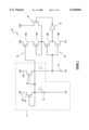
- FIG. 1 is a simplified block diagram of the preferred embodiment of the voltage independent time delay circuit of the present invention.
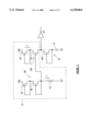
- FIG. 2 is a simplified block diagram of an alternate embodiment of the voltage independent time delay circuit of the present invention.
- the circuit 10 is comprised of a current mirror circuit 12, a capacitor 14, an inverter 18 and a voltage shift circuit 24.
- the circuit 10 uses a current mirror circuit 12 in order to charge a capacitor 14 in a linear manner.
- Capacitor 14 has a first terminal connected to the current mirror circuit and to inverter 18 and a second terminal connected to the ground.
- the current mirror circuit 12 is comprised of two conduction paths 12A and 12B.
- the current mirror circuit 12 generates a current I 1 in a first conduction path 12A and mirrors the current I 1 in a second conduction path 12B of current mirror circuit 12.
- the current I 1 in the second conduction path 12B of the current mirror circuit 12 is used to charge a capacitor 14 in a linear manner. When the capacitor 14 has been sufficiently charged, the voltage level at the input of the inverter 18 will cause the inverter 18 to trip ending the delay time of the circuit 10.
- the inverter 18 is a standard inverter, which is comprised of a P-channel transistor 18A which is coupled to an N-channel transistor 18B.
- P-channel transistor 18A has a first terminal connected to the first terminal of transistor 18B and to the transistor 22.
- the second terminal of transistor 18A is connected to a second terminal of transistor 18B.
- the third terminal of transistor 18B is connected to ground.
- the current mirror circuit 12 has a first branch 12A and a second branch 12B.
- the first branch 12A has a P-channel diode connected transistor 20.
- Transistor 20 is coupled to a voltage source V dd .
- a resistor 16 has a first terminal coupled to the transistor 20 and a second terminal coupled to the ground.
- the second branch 12B has a P-channel transistor 22.
- the transistor 22 has a first terminal coupled to the voltage source V dd and a second terminal coupled to the transistor 20.
- the function of the circuit 10 is described below. To ensure that the circuit 10 does not change with the voltage source V dd , the associated current and delay equations must be considered.
- the current I 1 in the current mirror circuit 12 may be defined as follows:
- I 1 is the current in each branch of the current mirror circuit 12
- V dd is the voltage of the voltage source
- V tp is the voltage drop across a transistor, in this case transistor 20, and R is the value of the resistor 16.
- the precise value of V tp can be controlled as part of the fabrication process. Since the current I 1 is used to charge the capacitor 14, the delay of the circuit 10 may be defined as:
- Delay is the delay of the circuit 10
- V dd /2 is the predetermined trip point of inverter 18
- I 1 is the current in each branch of the current mirror circuit 12.
- the V dd in the numerator of equation (4) must be equal to (V dd -V tp ). This means that the trip point of the inverter 18 must shift by a voltage equal to V tp . If the V dd in the numerator of equation (4) is equal to (V dd -V tp ), then the delay is equal to:
- the circuit 10 generates a delay time that is independent of the voltage V dd .
- a voltage shift circuit 24 is used to shift the trip point of the inverter 18 by a voltage equal to V tp .
- the voltage shift circuit 24 consists of a P-channel transistor 24A and a P-channel diode connected transistor 24B.
- Transistor 24A has a first terminal connected to the voltage source V dd and a second terminal connected to the transistor 22.
- Transistor 24B has a first terminal connected to transistor 24A and a second terminal connected to transistor 26 and to transistor 18A.
- Transistors 24A and 24B are designed to shift the trip point of the inverter 18 by a voltage equal to V tp .
- the V tp across transistor 24B must be the same as the V tp across transistor 20.
- Transistor 24A causes this by further mirroring current I 1 into transistor 24B. The result is that the delay of the circuit 10 is independent of the voltage source V dd .
- inverter 18 can now only drive a high level (V dd -V tp ) P channel transistor 26 and the inverter 27 are used to change the high state output of the inverter 18 to V dd , once the delay is complete.
- Inverter 27 has a first terminal connected to the second terminal of transistor 18A.
- P-channel transistor 26 has a first terminal coupled to inverter 27 and a second terminal coupled to a voltage source V dd .
- FIG. 2 represents a second embodiment of the voltage independent time delay circuit 10, wherein like numerals and symbols represent like elements with the exception of use of "'".
- the circuit 10' uses a current mirror circuit 12' with two conduction paths to charge the capacitor 14' in a linear manner.
- the first conduction path 12A' has two P-channel diode connected transistors 20' and 25'.
- the transistor 25' has the first terminal coupled to a voltage source V dd ' and the second terminal coupled to the transistor 20'.
- a resistor 16' has a first terminal coupled to transistor 20' and a second terminal coupled to ground.
- the second conduction path 12B' has a P-channel diode connected transistor 26' and a P-channel transistor 22'.
- the transistor 26' has a first terminal coupled to the voltage source V dd '.
- the transistor 22' has a first terminal coupled to a transistor 26'.
- a second terminal of the transistor 22' is coupled to the diode connected transistor 20'.
- a third terminal of the transistor 22' is coupled to the inverter 18'.
- a P-channel diode connected transistor 24A' has a first terminal coupled to the inverter 18' and to the current mirror circuit and a second terminal coupled to the capacitor 14'.
- the capacitor 14' has a first terminal coupled to the transistor 24A' and a second terminal coupled to ground.
- An inverter 18' is coupled to the current mirror circuit 12'.
- the inverter 18' is a standard inverter comprising of a P-channel transistor coupled to an N-channel transistor.
- the current mirror circuit 12' generates a current I 1 ' in a first conduction path 12A' and mirrors the current I 1 ' in a second conduction path 12B' of the current mirror circuit 12'.
- the current I 1 ' in the second branch 12B' of the current mirror circuit 12 charges capacitor 14'. When the capacitor 14' has been sufficiently charged, the voltage level at the input of the inverter 18' will cause inverter 18' to trip, ending the delay time of the circuit 10'.
- the size of the capacitor 14' in conjunction with the size of a resistor 16' in the current mirror circuit 12' is used to determine the delay time of the circuit 10'.
- circuit 10' of FIG. 2 functions in accordance with the equations put forward below.
- I 1 ' is the current in each branch of the current mirror circuit 12'
- V dd is the voltage of the voltage source
- V tp is the voltage drop across a transistor, in this case transistor 20'
- R' is the value of the resistor 16'. Since the current I 1 ' is used to charge the capacitor 14', the delay of the circuit 10' may be defined as:
- Delay is the delay of the circuit 10'
- V dd /2 is the predetermined trip point of inverter 18
- I 1 ' is the current in each branch of the current mirror circuit 12'.
- the circuit 10' generates a delay time that is independent of the voltage V dd .
Landscapes
- Physics & Mathematics (AREA)
- Nonlinear Science (AREA)
- Pulse Circuits (AREA)
Abstract
Description
I.sub.1 =(V.sub.dd -V.sub.tp)/R (1)
Delay=C*(V.sub.dd /2)/I.sub.1 (2)
Delay=C*(V.sub.dd /2)/((V.sub.dd -V.sub.tp)/R) (3)
Delay=R*(C/2)*V.sub.dd /(V.sub.dd -V.sub.tp) (4)
Delay=R*C/2*(V.sub.dd -V.sub.tp)/(V.sub.dd -V.sub.tp) (5)
Delay=R*C/2 (6)
I.sub.1 '=(V.sub.dd -2V.sub.tp)/R' (7)
Delay=C'*(V.sub.dd /2)/I.sub.1 ' (8)
Delay=C'*(V.sub.dd /2-V.sub.tp)/I.sub.1 ' (9)
Delay=C'*(V.sub.dd /2-V.sub.tp)/((V.sub.dd -2V.sub.tp)/R') (10)
Delay=2*R'*C'*(V.sub.dd -2V.sub.tp)/(V.sub.dd -2V.sub.tp) (11)
Delay=2*R'*C' (12)
Claims (12)
Priority Applications (1)
| Application Number | Priority Date | Filing Date | Title |
|---|---|---|---|
| US09/138,714 US6150864A (en) | 1998-08-24 | 1998-08-24 | Time delay circuit which is voltage independent |
Applications Claiming Priority (1)
| Application Number | Priority Date | Filing Date | Title |
|---|---|---|---|
| US09/138,714 US6150864A (en) | 1998-08-24 | 1998-08-24 | Time delay circuit which is voltage independent |
Publications (1)
| Publication Number | Publication Date |
|---|---|
| US6150864A true US6150864A (en) | 2000-11-21 |
Family
ID=22483289
Family Applications (1)
| Application Number | Title | Priority Date | Filing Date |
|---|---|---|---|
| US09/138,714 Expired - Lifetime US6150864A (en) | 1998-08-24 | 1998-08-24 | Time delay circuit which is voltage independent |
Country Status (1)
| Country | Link |
|---|---|
| US (1) | US6150864A (en) |
Cited By (5)
| Publication number | Priority date | Publication date | Assignee | Title |
|---|---|---|---|---|
| US6624680B2 (en) * | 2000-12-29 | 2003-09-23 | Texas Instruments Incorporated | Reduction of propagation delay dependence on supply voltage in a digital circuit |
| US20030193359A1 (en) * | 2002-04-12 | 2003-10-16 | Ji-Ho Cho | Semiconductor memory delay circuit |
| US6657889B1 (en) | 2002-06-28 | 2003-12-02 | Motorola, Inc. | Memory having write current ramp rate control |
| US20120249221A1 (en) * | 2011-03-28 | 2012-10-04 | Hynix Semiconductor Inc. | Semiconductor integrated circuit |
| US9177622B2 (en) | 2012-02-14 | 2015-11-03 | Micron Technology, Inc. | Supply independent delayer |
Citations (3)
| Publication number | Priority date | Publication date | Assignee | Title |
|---|---|---|---|---|
| US5057722A (en) * | 1989-06-20 | 1991-10-15 | Nec Corporation | Delay circuit having stable delay time |
| US5926042A (en) * | 1997-12-19 | 1999-07-20 | Advanced Micro Devices, Inc. | Precision clock frequency detector having reduced supply voltage dependence |
| US5929681A (en) * | 1997-03-19 | 1999-07-27 | Fujitsu Limited | Delay circuit applied to semiconductor memory device having auto power-down function |
-
1998
- 1998-08-24 US US09/138,714 patent/US6150864A/en not_active Expired - Lifetime
Patent Citations (3)
| Publication number | Priority date | Publication date | Assignee | Title |
|---|---|---|---|---|
| US5057722A (en) * | 1989-06-20 | 1991-10-15 | Nec Corporation | Delay circuit having stable delay time |
| US5929681A (en) * | 1997-03-19 | 1999-07-27 | Fujitsu Limited | Delay circuit applied to semiconductor memory device having auto power-down function |
| US5926042A (en) * | 1997-12-19 | 1999-07-20 | Advanced Micro Devices, Inc. | Precision clock frequency detector having reduced supply voltage dependence |
Cited By (7)
| Publication number | Priority date | Publication date | Assignee | Title |
|---|---|---|---|---|
| US6624680B2 (en) * | 2000-12-29 | 2003-09-23 | Texas Instruments Incorporated | Reduction of propagation delay dependence on supply voltage in a digital circuit |
| US20030193359A1 (en) * | 2002-04-12 | 2003-10-16 | Ji-Ho Cho | Semiconductor memory delay circuit |
| US6867628B2 (en) * | 2002-04-12 | 2005-03-15 | Samsung Electronics Co. Ltd. | Semiconductor memory delay circuit |
| US6657889B1 (en) | 2002-06-28 | 2003-12-02 | Motorola, Inc. | Memory having write current ramp rate control |
| US20120249221A1 (en) * | 2011-03-28 | 2012-10-04 | Hynix Semiconductor Inc. | Semiconductor integrated circuit |
| US8598943B2 (en) * | 2011-03-28 | 2013-12-03 | SK Hynix Inc. | Semiconductor integrated circuit with stable rupture voltage fuse |
| US9177622B2 (en) | 2012-02-14 | 2015-11-03 | Micron Technology, Inc. | Supply independent delayer |
Similar Documents
| Publication | Publication Date | Title |
|---|---|---|
| US5640122A (en) | Circuit for providing a bias voltage compensated for p-channel transistor variations | |
| KR0132641B1 (en) | Substrate circuit | |
| JP3476363B2 (en) | Bandgap reference voltage generator | |
| KR100218078B1 (en) | Substrate potential generating circuit that can suppress fluctuations in output voltage due to fluctuations in external power supply voltage or changes in environmental temperature | |
| US6201436B1 (en) | Bias current generating circuits and methods for integrated circuits including bias current generators that increase and decrease with temperature | |
| US6388507B1 (en) | Voltage to current converter with variation-free MOS resistor | |
| JPH047609B2 (en) | ||
| US4894560A (en) | Dual-slope waveform generation circuit | |
| KR910015114A (en) | Semiconductor digital circuits | |
| US5929679A (en) | Voltage monitoring circuit capable of reducing power dissipation | |
| KR0126911B1 (en) | Circuit and method for voltage reference generating | |
| KR100848740B1 (en) | Reference voltage circuit | |
| US6150864A (en) | Time delay circuit which is voltage independent | |
| US6380792B1 (en) | Semiconductor integrated circuit | |
| KR960003087A (en) | Crystal oscillation circuit | |
| US5510750A (en) | Bias circuit for providing a stable output current | |
| KR100363139B1 (en) | Buffer Circuit and Bias Circuit | |
| EP0651311A2 (en) | Self-exciting constant current circuit | |
| JP2746117B2 (en) | Substrate bias circuit | |
| JP2994114B2 (en) | Program circuit | |
| KR100258362B1 (en) | Reference voltage generator of semiconductor device | |
| KR100243263B1 (en) | Schmitt trigger circuit for RC oscillator | |
| JP2964775B2 (en) | Reference voltage generation circuit | |
| KR100215761B1 (en) | Level shift circuit in semiconductor memory device | |
| KR100489587B1 (en) | Time delay circuit |
Legal Events
| Date | Code | Title | Description |
|---|---|---|---|
| AS | Assignment |
Owner name: MICROCHIP TECHNOLOGY INCORPORATED, ARIZONA Free format text: ASSIGNMENT OF ASSIGNORS INTEREST;ASSIGNORS:YACH, RANDY L.;HEWITT, KENT;SUSAK, DAVID M.;REEL/FRAME:009421/0582;SIGNING DATES FROM 19980820 TO 19980821 |
|
| STCF | Information on status: patent grant |
Free format text: PATENTED CASE |
|
| FEPP | Fee payment procedure |
Free format text: PAYOR NUMBER ASSIGNED (ORIGINAL EVENT CODE: ASPN); ENTITY STATUS OF PATENT OWNER: LARGE ENTITY |
|
| FPAY | Fee payment |
Year of fee payment: 4 |
|
| FPAY | Fee payment |
Year of fee payment: 8 |
|
| FPAY | Fee payment |
Year of fee payment: 12 |
|
| AS | Assignment |
Owner name: JPMORGAN CHASE BANK, N.A., AS ADMINISTRATIVE AGENT, ILLINOIS Free format text: SECURITY INTEREST;ASSIGNOR:MICROCHIP TECHNOLOGY INCORPORATED;REEL/FRAME:041675/0617 Effective date: 20170208 Owner name: JPMORGAN CHASE BANK, N.A., AS ADMINISTRATIVE AGENT Free format text: SECURITY INTEREST;ASSIGNOR:MICROCHIP TECHNOLOGY INCORPORATED;REEL/FRAME:041675/0617 Effective date: 20170208 |
|
| AS | Assignment |
Owner name: JPMORGAN CHASE BANK, N.A., AS ADMINISTRATIVE AGENT, ILLINOIS Free format text: SECURITY INTEREST;ASSIGNORS:MICROCHIP TECHNOLOGY INCORPORATED;SILICON STORAGE TECHNOLOGY, INC.;ATMEL CORPORATION;AND OTHERS;REEL/FRAME:046426/0001 Effective date: 20180529 Owner name: JPMORGAN CHASE BANK, N.A., AS ADMINISTRATIVE AGENT Free format text: SECURITY INTEREST;ASSIGNORS:MICROCHIP TECHNOLOGY INCORPORATED;SILICON STORAGE TECHNOLOGY, INC.;ATMEL CORPORATION;AND OTHERS;REEL/FRAME:046426/0001 Effective date: 20180529 |
|
| AS | Assignment |
Owner name: WELLS FARGO BANK, NATIONAL ASSOCIATION, AS NOTES COLLATERAL AGENT, CALIFORNIA Free format text: SECURITY INTEREST;ASSIGNORS:MICROCHIP TECHNOLOGY INCORPORATED;SILICON STORAGE TECHNOLOGY, INC.;ATMEL CORPORATION;AND OTHERS;REEL/FRAME:047103/0206 Effective date: 20180914 Owner name: WELLS FARGO BANK, NATIONAL ASSOCIATION, AS NOTES C Free format text: SECURITY INTEREST;ASSIGNORS:MICROCHIP TECHNOLOGY INCORPORATED;SILICON STORAGE TECHNOLOGY, INC.;ATMEL CORPORATION;AND OTHERS;REEL/FRAME:047103/0206 Effective date: 20180914 |
|
| AS | Assignment |
Owner name: MICROSEMI STORAGE SOLUTIONS, INC., ARIZONA Free format text: RELEASE BY SECURED PARTY;ASSIGNOR:JPMORGAN CHASE BANK, N.A., AS ADMINISTRATIVE AGENT;REEL/FRAME:059333/0222 Effective date: 20220218 Owner name: MICROSEMI CORPORATION, ARIZONA Free format text: RELEASE BY SECURED PARTY;ASSIGNOR:JPMORGAN CHASE BANK, N.A., AS ADMINISTRATIVE AGENT;REEL/FRAME:059333/0222 Effective date: 20220218 Owner name: ATMEL CORPORATION, ARIZONA Free format text: RELEASE BY SECURED PARTY;ASSIGNOR:JPMORGAN CHASE BANK, N.A., AS ADMINISTRATIVE AGENT;REEL/FRAME:059333/0222 Effective date: 20220218 Owner name: SILICON STORAGE TECHNOLOGY, INC., ARIZONA Free format text: RELEASE BY SECURED PARTY;ASSIGNOR:JPMORGAN CHASE BANK, N.A., AS ADMINISTRATIVE AGENT;REEL/FRAME:059333/0222 Effective date: 20220218 Owner name: MICROCHIP TECHNOLOGY INCORPORATED, ARIZONA Free format text: RELEASE BY SECURED PARTY;ASSIGNOR:JPMORGAN CHASE BANK, N.A., AS ADMINISTRATIVE AGENT;REEL/FRAME:059333/0222 Effective date: 20220218 Owner name: MICROCHIP TECHNOLOGY INCORPORATED, ARIZONA Free format text: RELEASE OF SECURITY INTEREST;ASSIGNOR:JPMORGAN CHASE BANK, N.A., AS ADMINISTRATIVE AGENT;REEL/FRAME:059333/0222 Effective date: 20220218 Owner name: SILICON STORAGE TECHNOLOGY, INC., ARIZONA Free format text: RELEASE OF SECURITY INTEREST;ASSIGNOR:JPMORGAN CHASE BANK, N.A., AS ADMINISTRATIVE AGENT;REEL/FRAME:059333/0222 Effective date: 20220218 Owner name: ATMEL CORPORATION, ARIZONA Free format text: RELEASE OF SECURITY INTEREST;ASSIGNOR:JPMORGAN CHASE BANK, N.A., AS ADMINISTRATIVE AGENT;REEL/FRAME:059333/0222 Effective date: 20220218 Owner name: MICROSEMI CORPORATION, ARIZONA Free format text: RELEASE OF SECURITY INTEREST;ASSIGNOR:JPMORGAN CHASE BANK, N.A., AS ADMINISTRATIVE AGENT;REEL/FRAME:059333/0222 Effective date: 20220218 Owner name: MICROSEMI STORAGE SOLUTIONS, INC., ARIZONA Free format text: RELEASE OF SECURITY INTEREST;ASSIGNOR:JPMORGAN CHASE BANK, N.A., AS ADMINISTRATIVE AGENT;REEL/FRAME:059333/0222 Effective date: 20220218 |
|
| AS | Assignment |
Owner name: MICROCHIP TECHNOLOGY INCORPORATED, ARIZONA Free format text: RELEASE BY SECURED PARTY;ASSIGNOR:JPMORGAN CHASE BANK, N.A., AS ADMINISTRATIVE AGENT;REEL/FRAME:059666/0545 Effective date: 20220218 |
|
| AS | Assignment |
Owner name: MICROSEMI STORAGE SOLUTIONS, INC., ARIZONA Free format text: RELEASE BY SECURED PARTY;ASSIGNOR:WELLS FARGO BANK, NATIONAL ASSOCIATION, AS NOTES COLLATERAL AGENT;REEL/FRAME:059358/0001 Effective date: 20220228 Owner name: MICROSEMI CORPORATION, ARIZONA Free format text: RELEASE BY SECURED PARTY;ASSIGNOR:WELLS FARGO BANK, NATIONAL ASSOCIATION, AS NOTES COLLATERAL AGENT;REEL/FRAME:059358/0001 Effective date: 20220228 Owner name: ATMEL CORPORATION, ARIZONA Free format text: RELEASE BY SECURED PARTY;ASSIGNOR:WELLS FARGO BANK, NATIONAL ASSOCIATION, AS NOTES COLLATERAL AGENT;REEL/FRAME:059358/0001 Effective date: 20220228 Owner name: SILICON STORAGE TECHNOLOGY, INC., ARIZONA Free format text: RELEASE BY SECURED PARTY;ASSIGNOR:WELLS FARGO BANK, NATIONAL ASSOCIATION, AS NOTES COLLATERAL AGENT;REEL/FRAME:059358/0001 Effective date: 20220228 Owner name: MICROCHIP TECHNOLOGY INCORPORATED, ARIZONA Free format text: RELEASE BY SECURED PARTY;ASSIGNOR:WELLS FARGO BANK, NATIONAL ASSOCIATION, AS NOTES COLLATERAL AGENT;REEL/FRAME:059358/0001 Effective date: 20220228 Owner name: MICROCHIP TECHNOLOGY INCORPORATED, ARIZONA Free format text: RELEASE OF SECURITY INTEREST;ASSIGNOR:WELLS FARGO BANK, NATIONAL ASSOCIATION, AS NOTES COLLATERAL AGENT;REEL/FRAME:059358/0001 Effective date: 20220228 Owner name: SILICON STORAGE TECHNOLOGY, INC., ARIZONA Free format text: RELEASE OF SECURITY INTEREST;ASSIGNOR:WELLS FARGO BANK, NATIONAL ASSOCIATION, AS NOTES COLLATERAL AGENT;REEL/FRAME:059358/0001 Effective date: 20220228 Owner name: ATMEL CORPORATION, ARIZONA Free format text: RELEASE OF SECURITY INTEREST;ASSIGNOR:WELLS FARGO BANK, NATIONAL ASSOCIATION, AS NOTES COLLATERAL AGENT;REEL/FRAME:059358/0001 Effective date: 20220228 Owner name: MICROSEMI CORPORATION, ARIZONA Free format text: RELEASE OF SECURITY INTEREST;ASSIGNOR:WELLS FARGO BANK, NATIONAL ASSOCIATION, AS NOTES COLLATERAL AGENT;REEL/FRAME:059358/0001 Effective date: 20220228 Owner name: MICROSEMI STORAGE SOLUTIONS, INC., ARIZONA Free format text: RELEASE OF SECURITY INTEREST;ASSIGNOR:WELLS FARGO BANK, NATIONAL ASSOCIATION, AS NOTES COLLATERAL AGENT;REEL/FRAME:059358/0001 Effective date: 20220228 |