US6150243A - Shallow junction formation by out-diffusion from a doped dielectric layer through a salicide layer - Google Patents
Shallow junction formation by out-diffusion from a doped dielectric layer through a salicide layer Download PDFInfo
- Publication number
- US6150243A US6150243A US09/186,065 US18606598A US6150243A US 6150243 A US6150243 A US 6150243A US 18606598 A US18606598 A US 18606598A US 6150243 A US6150243 A US 6150243A
- Authority
- US
- United States
- Prior art keywords
- layer
- silicon
- metal silicide
- portions
- metal
- Prior art date
- Legal status (The legal status is an assumption and is not a legal conclusion. Google has not performed a legal analysis and makes no representation as to the accuracy of the status listed.)
- Expired - Lifetime
Links
- 238000009792 diffusion process Methods 0.000 title claims abstract description 8
- 230000015572 biosynthetic process Effects 0.000 title description 11
- 229910052751 metal Inorganic materials 0.000 claims abstract description 90
- 239000002184 metal Substances 0.000 claims abstract description 90
- 229910021332 silicide Inorganic materials 0.000 claims abstract description 72
- FVBUAEGBCNSCDD-UHFFFAOYSA-N silicide(4-) Chemical compound [Si-4] FVBUAEGBCNSCDD-UHFFFAOYSA-N 0.000 claims abstract description 69
- 229910052710 silicon Inorganic materials 0.000 claims abstract description 66
- 239000010703 silicon Substances 0.000 claims abstract description 66
- XUIMIQQOPSSXEZ-UHFFFAOYSA-N Silicon Chemical compound [Si] XUIMIQQOPSSXEZ-UHFFFAOYSA-N 0.000 claims abstract description 60
- 239000000758 substrate Substances 0.000 claims abstract description 45
- 239000002019 doping agent Substances 0.000 claims abstract description 30
- 150000002500 ions Chemical class 0.000 claims abstract description 15
- 238000000034 method Methods 0.000 claims description 55
- 239000010941 cobalt Substances 0.000 claims description 24
- 229910017052 cobalt Inorganic materials 0.000 claims description 24
- GUTLYIVDDKVIGB-UHFFFAOYSA-N cobalt atom Chemical compound [Co] GUTLYIVDDKVIGB-UHFFFAOYSA-N 0.000 claims description 24
- 239000004065 semiconductor Substances 0.000 claims description 24
- 229910052814 silicon oxide Inorganic materials 0.000 claims description 18
- VYPSYNLAJGMNEJ-UHFFFAOYSA-N Silicium dioxide Chemical compound O=[Si]=O VYPSYNLAJGMNEJ-UHFFFAOYSA-N 0.000 claims description 17
- 238000002955 isolation Methods 0.000 claims description 16
- 125000006850 spacer group Chemical group 0.000 claims description 15
- 238000010438 heat treatment Methods 0.000 claims description 14
- PXHVJJICTQNCMI-UHFFFAOYSA-N Nickel Chemical compound [Ni] PXHVJJICTQNCMI-UHFFFAOYSA-N 0.000 claims description 12
- 239000002243 precursor Substances 0.000 claims description 12
- 239000012535 impurity Substances 0.000 claims description 11
- 238000004519 manufacturing process Methods 0.000 claims description 9
- 238000006243 chemical reaction Methods 0.000 claims description 8
- 238000002513 implantation Methods 0.000 claims description 8
- 229910052581 Si3N4 Inorganic materials 0.000 claims description 7
- 239000010936 titanium Substances 0.000 claims description 7
- RTAQQCXQSZGOHL-UHFFFAOYSA-N Titanium Chemical compound [Ti] RTAQQCXQSZGOHL-UHFFFAOYSA-N 0.000 claims description 6
- 239000003989 dielectric material Substances 0.000 claims description 6
- 229910052759 nickel Inorganic materials 0.000 claims description 6
- HQVNEWCFYHHQES-UHFFFAOYSA-N silicon nitride Chemical compound N12[Si]34N5[Si]62N3[Si]51N64 HQVNEWCFYHHQES-UHFFFAOYSA-N 0.000 claims description 6
- -1 silicon nitrides Chemical class 0.000 claims description 6
- 229910052719 titanium Inorganic materials 0.000 claims description 6
- 229910021420 polycrystalline silicon Inorganic materials 0.000 claims description 4
- 229920005591 polysilicon Polymers 0.000 claims description 4
- ZOXJGFHDIHLPTG-UHFFFAOYSA-N Boron Chemical compound [B] ZOXJGFHDIHLPTG-UHFFFAOYSA-N 0.000 claims description 3
- 229910052796 boron Inorganic materials 0.000 claims description 3
- 238000005468 ion implantation Methods 0.000 claims description 3
- 230000001788 irregular Effects 0.000 claims description 3
- OAICVXFJPJFONN-UHFFFAOYSA-N Phosphorus Chemical compound [P] OAICVXFJPJFONN-UHFFFAOYSA-N 0.000 claims description 2
- 229910052785 arsenic Inorganic materials 0.000 claims description 2
- RQNWIZPPADIBDY-UHFFFAOYSA-N arsenic atom Chemical compound [As] RQNWIZPPADIBDY-UHFFFAOYSA-N 0.000 claims description 2
- 239000000463 material Substances 0.000 claims description 2
- 229910052698 phosphorus Inorganic materials 0.000 claims description 2
- 239000011574 phosphorus Substances 0.000 claims description 2
- 238000009413 insulation Methods 0.000 claims 2
- 229910018999 CoSi2 Inorganic materials 0.000 claims 1
- 239000007943 implant Substances 0.000 claims 1
- 230000000149 penetrating effect Effects 0.000 claims 1
- 238000007669 thermal treatment Methods 0.000 abstract description 3
- 239000003870 refractory metal Substances 0.000 description 19
- 230000008569 process Effects 0.000 description 18
- 238000004151 rapid thermal annealing Methods 0.000 description 13
- 230000008901 benefit Effects 0.000 description 9
- 238000012545 processing Methods 0.000 description 9
- 238000000151 deposition Methods 0.000 description 6
- 229910021341 titanium silicide Inorganic materials 0.000 description 6
- 230000008021 deposition Effects 0.000 description 5
- 238000005516 engineering process Methods 0.000 description 4
- 230000035515 penetration Effects 0.000 description 4
- 238000000137 annealing Methods 0.000 description 3
- 238000007796 conventional method Methods 0.000 description 3
- 230000007423 decrease Effects 0.000 description 3
- 238000013461 design Methods 0.000 description 3
- 230000000694 effects Effects 0.000 description 3
- 230000010354 integration Effects 0.000 description 3
- 230000007246 mechanism Effects 0.000 description 3
- 229910019001 CoSi Inorganic materials 0.000 description 2
- 229910012990 NiSi2 Inorganic materials 0.000 description 2
- 238000013459 approach Methods 0.000 description 2
- 238000010586 diagram Methods 0.000 description 2
- 150000002739 metals Chemical class 0.000 description 2
- 238000012986 modification Methods 0.000 description 2
- 230000004048 modification Effects 0.000 description 2
- 238000005457 optimization Methods 0.000 description 2
- 238000005240 physical vapour deposition Methods 0.000 description 2
- NRTOMJZYCJJWKI-UHFFFAOYSA-N Titanium nitride Chemical compound [Ti]#N NRTOMJZYCJJWKI-UHFFFAOYSA-N 0.000 description 1
- 229910021417 amorphous silicon Inorganic materials 0.000 description 1
- 230000001419 dependent effect Effects 0.000 description 1
- 238000005530 etching Methods 0.000 description 1
- 230000001747 exhibiting effect Effects 0.000 description 1
- 229910052732 germanium Inorganic materials 0.000 description 1
- GNPVGFCGXDBREM-UHFFFAOYSA-N germanium atom Chemical compound [Ge] GNPVGFCGXDBREM-UHFFFAOYSA-N 0.000 description 1
- 229910000765 intermetallic Inorganic materials 0.000 description 1
- 238000001755 magnetron sputter deposition Methods 0.000 description 1
- 229910021421 monocrystalline silicon Inorganic materials 0.000 description 1
- 230000003647 oxidation Effects 0.000 description 1
- 238000007254 oxidation reaction Methods 0.000 description 1
- 230000002265 prevention Effects 0.000 description 1
- 239000000376 reactant Substances 0.000 description 1
- 230000009467 reduction Effects 0.000 description 1
- 238000005204 segregation Methods 0.000 description 1
- LIVNPJMFVYWSIS-UHFFFAOYSA-N silicon monoxide Chemical class [Si-]#[O+] LIVNPJMFVYWSIS-UHFFFAOYSA-N 0.000 description 1
- 238000004544 sputter deposition Methods 0.000 description 1
- 238000005477 sputtering target Methods 0.000 description 1
- 238000012546 transfer Methods 0.000 description 1
Images
Classifications
-
- H—ELECTRICITY
- H01—ELECTRIC ELEMENTS
- H01L—SEMICONDUCTOR DEVICES NOT COVERED BY CLASS H10
- H01L21/00—Processes or apparatus adapted for the manufacture or treatment of semiconductor or solid state devices or of parts thereof
- H01L21/02—Manufacture or treatment of semiconductor devices or of parts thereof
- H01L21/04—Manufacture or treatment of semiconductor devices or of parts thereof the devices having at least one potential-jump barrier or surface barrier, e.g. PN junction, depletion layer or carrier concentration layer
- H01L21/18—Manufacture or treatment of semiconductor devices or of parts thereof the devices having at least one potential-jump barrier or surface barrier, e.g. PN junction, depletion layer or carrier concentration layer the devices having semiconductor bodies comprising elements of Group IV of the Periodic System or AIIIBV compounds with or without impurities, e.g. doping materials
- H01L21/26—Bombardment with radiation
- H01L21/263—Bombardment with radiation with high-energy radiation
- H01L21/265—Bombardment with radiation with high-energy radiation producing ion implantation
- H01L21/26506—Bombardment with radiation with high-energy radiation producing ion implantation in group IV semiconductors
- H01L21/26513—Bombardment with radiation with high-energy radiation producing ion implantation in group IV semiconductors of electrically active species
- H01L21/2652—Through-implantation
-
- H—ELECTRICITY
- H01—ELECTRIC ELEMENTS
- H01L—SEMICONDUCTOR DEVICES NOT COVERED BY CLASS H10
- H01L21/00—Processes or apparatus adapted for the manufacture or treatment of semiconductor or solid state devices or of parts thereof
- H01L21/02—Manufacture or treatment of semiconductor devices or of parts thereof
- H01L21/04—Manufacture or treatment of semiconductor devices or of parts thereof the devices having at least one potential-jump barrier or surface barrier, e.g. PN junction, depletion layer or carrier concentration layer
- H01L21/18—Manufacture or treatment of semiconductor devices or of parts thereof the devices having at least one potential-jump barrier or surface barrier, e.g. PN junction, depletion layer or carrier concentration layer the devices having semiconductor bodies comprising elements of Group IV of the Periodic System or AIIIBV compounds with or without impurities, e.g. doping materials
- H01L21/22—Diffusion of impurity materials, e.g. doping materials, electrode materials, into or out of a semiconductor body, or between semiconductor regions; Interactions between two or more impurities; Redistribution of impurities
- H01L21/225—Diffusion of impurity materials, e.g. doping materials, electrode materials, into or out of a semiconductor body, or between semiconductor regions; Interactions between two or more impurities; Redistribution of impurities using diffusion into or out of a solid from or into a solid phase, e.g. a doped oxide layer
- H01L21/2251—Diffusion into or out of group IV semiconductors
- H01L21/2254—Diffusion into or out of group IV semiconductors from or through or into an applied layer, e.g. photoresist, nitrides
- H01L21/2255—Diffusion into or out of group IV semiconductors from or through or into an applied layer, e.g. photoresist, nitrides the applied layer comprising oxides only, e.g. P2O5, PSG, H3BO3, doped oxides
-
- H—ELECTRICITY
- H01—ELECTRIC ELEMENTS
- H01L—SEMICONDUCTOR DEVICES NOT COVERED BY CLASS H10
- H01L21/00—Processes or apparatus adapted for the manufacture or treatment of semiconductor or solid state devices or of parts thereof
- H01L21/02—Manufacture or treatment of semiconductor devices or of parts thereof
- H01L21/04—Manufacture or treatment of semiconductor devices or of parts thereof the devices having at least one potential-jump barrier or surface barrier, e.g. PN junction, depletion layer or carrier concentration layer
- H01L21/18—Manufacture or treatment of semiconductor devices or of parts thereof the devices having at least one potential-jump barrier or surface barrier, e.g. PN junction, depletion layer or carrier concentration layer the devices having semiconductor bodies comprising elements of Group IV of the Periodic System or AIIIBV compounds with or without impurities, e.g. doping materials
- H01L21/22—Diffusion of impurity materials, e.g. doping materials, electrode materials, into or out of a semiconductor body, or between semiconductor regions; Interactions between two or more impurities; Redistribution of impurities
- H01L21/225—Diffusion of impurity materials, e.g. doping materials, electrode materials, into or out of a semiconductor body, or between semiconductor regions; Interactions between two or more impurities; Redistribution of impurities using diffusion into or out of a solid from or into a solid phase, e.g. a doped oxide layer
- H01L21/2251—Diffusion into or out of group IV semiconductors
- H01L21/2254—Diffusion into or out of group IV semiconductors from or through or into an applied layer, e.g. photoresist, nitrides
- H01L21/2257—Diffusion into or out of group IV semiconductors from or through or into an applied layer, e.g. photoresist, nitrides the applied layer being silicon or silicide or SIPOS, e.g. polysilicon, porous silicon
-
- H—ELECTRICITY
- H01—ELECTRIC ELEMENTS
- H01L—SEMICONDUCTOR DEVICES NOT COVERED BY CLASS H10
- H01L21/00—Processes or apparatus adapted for the manufacture or treatment of semiconductor or solid state devices or of parts thereof
- H01L21/02—Manufacture or treatment of semiconductor devices or of parts thereof
- H01L21/04—Manufacture or treatment of semiconductor devices or of parts thereof the devices having at least one potential-jump barrier or surface barrier, e.g. PN junction, depletion layer or carrier concentration layer
- H01L21/18—Manufacture or treatment of semiconductor devices or of parts thereof the devices having at least one potential-jump barrier or surface barrier, e.g. PN junction, depletion layer or carrier concentration layer the devices having semiconductor bodies comprising elements of Group IV of the Periodic System or AIIIBV compounds with or without impurities, e.g. doping materials
- H01L21/28—Manufacture of electrodes on semiconductor bodies using processes or apparatus not provided for in groups H01L21/20 - H01L21/268
- H01L21/28008—Making conductor-insulator-semiconductor electrodes
- H01L21/28017—Making conductor-insulator-semiconductor electrodes the insulator being formed after the semiconductor body, the semiconductor being silicon
- H01L21/28026—Making conductor-insulator-semiconductor electrodes the insulator being formed after the semiconductor body, the semiconductor being silicon characterised by the conductor
- H01L21/28035—Making conductor-insulator-semiconductor electrodes the insulator being formed after the semiconductor body, the semiconductor being silicon characterised by the conductor the final conductor layer next to the insulator being silicon, e.g. polysilicon, with or without impurities
- H01L21/28044—Making conductor-insulator-semiconductor electrodes the insulator being formed after the semiconductor body, the semiconductor being silicon characterised by the conductor the final conductor layer next to the insulator being silicon, e.g. polysilicon, with or without impurities the conductor comprising at least another non-silicon conductive layer
- H01L21/28061—Making conductor-insulator-semiconductor electrodes the insulator being formed after the semiconductor body, the semiconductor being silicon characterised by the conductor the final conductor layer next to the insulator being silicon, e.g. polysilicon, with or without impurities the conductor comprising at least another non-silicon conductive layer the conductor comprising a metal or metal silicide formed by deposition, e.g. sputter deposition, i.e. without a silicidation reaction
-
- H—ELECTRICITY
- H01—ELECTRIC ELEMENTS
- H01L—SEMICONDUCTOR DEVICES NOT COVERED BY CLASS H10
- H01L29/00—Semiconductor devices adapted for rectifying, amplifying, oscillating or switching, or capacitors or resistors with at least one potential-jump barrier or surface barrier, e.g. PN junction depletion layer or carrier concentration layer; Details of semiconductor bodies or of electrodes thereof ; Multistep manufacturing processes therefor
- H01L29/66—Types of semiconductor device ; Multistep manufacturing processes therefor
- H01L29/66007—Multistep manufacturing processes
- H01L29/66075—Multistep manufacturing processes of devices having semiconductor bodies comprising group 14 or group 13/15 materials
- H01L29/66227—Multistep manufacturing processes of devices having semiconductor bodies comprising group 14 or group 13/15 materials the devices being controllable only by the electric current supplied or the electric potential applied, to an electrode which does not carry the current to be rectified, amplified or switched, e.g. three-terminal devices
- H01L29/66409—Unipolar field-effect transistors
- H01L29/66477—Unipolar field-effect transistors with an insulated gate, i.e. MISFET
- H01L29/665—Unipolar field-effect transistors with an insulated gate, i.e. MISFET using self aligned silicidation, i.e. salicide
-
- H—ELECTRICITY
- H01—ELECTRIC ELEMENTS
- H01L—SEMICONDUCTOR DEVICES NOT COVERED BY CLASS H10
- H01L29/00—Semiconductor devices adapted for rectifying, amplifying, oscillating or switching, or capacitors or resistors with at least one potential-jump barrier or surface barrier, e.g. PN junction depletion layer or carrier concentration layer; Details of semiconductor bodies or of electrodes thereof ; Multistep manufacturing processes therefor
- H01L29/66—Types of semiconductor device ; Multistep manufacturing processes therefor
- H01L29/66007—Multistep manufacturing processes
- H01L29/66075—Multistep manufacturing processes of devices having semiconductor bodies comprising group 14 or group 13/15 materials
- H01L29/66227—Multistep manufacturing processes of devices having semiconductor bodies comprising group 14 or group 13/15 materials the devices being controllable only by the electric current supplied or the electric potential applied, to an electrode which does not carry the current to be rectified, amplified or switched, e.g. three-terminal devices
- H01L29/66409—Unipolar field-effect transistors
- H01L29/66477—Unipolar field-effect transistors with an insulated gate, i.e. MISFET
- H01L29/66568—Lateral single gate silicon transistors
- H01L29/66575—Lateral single gate silicon transistors where the source and drain or source and drain extensions are self-aligned to the sides of the gate
- H01L29/6659—Lateral single gate silicon transistors where the source and drain or source and drain extensions are self-aligned to the sides of the gate with both lightly doped source and drain extensions and source and drain self-aligned to the sides of the gate, e.g. lightly doped drain [LDD] MOSFET, double diffused drain [DDD] MOSFET
Definitions
- the present invention relates to a method of manufacturing high-density integrated semiconductor devices such as MOS transistors and CMOS devices formed in or on a semiconductor wafer substrate and having low resistance, ultra-shallow junctions forming low junction leakage source and drain regions by utilizing self-aligned, refractory metal silicide ("salicide”) processing.
- the invention has particular utility in manufacturing high-density integration semiconductor devices, including multi-level devices, with design rules of 0.18 micron and below.
- LDDs lightly doped drains
- An LDD consists of a lightly doped source/drain region (i.e., dopant density is on the order of about 9 ⁇ 10 19 da/cm 3 ) formed just at the edge of the gate region, while a more heavily doped drain region (i.e., dopant density is on the order of about 2 ⁇ 10 20 da/cm 3 ), to which ohmic contact is to be provided, is laterally displaced away from the gate by provision of a sidewall spacer on the gate electrode.
- dopant density is on the order of about 9 ⁇ 10 19 da/cm 3
- a more heavily doped drain region i.e., dopant density is on the order of about 2 ⁇ 10 20 da/cm 3
- Salicide processing involves deposition of a metal that forms an intermetallic compound with silicon, but does not react with silicon oxides or silicon nitrides under normal processing conditions.
- Refractory metals commonly employed in salicide processing include titanium, nickel, and cobalt, each of which form very low resistivity phases with silicon, e.g., TiSi 2 , NiSi 2 , and CoSi 2 .
- the refractory metal is deposited in a uniform thickness over all exposed upper surface features of the silicon wafer, preferably by means of physical vapor deposition (PVD) from an ultra-pure sputtering target and an ultra-high vacuum, multi-chamber DC magnetron sputtering system.
- PVD physical vapor deposition
- deposition is generally performed both after gate etch and after source/drain junction formation.
- the refractory metal blankets the polysilicon gate electrode, the silicon oxide or nitride spacers, the silicon oxide isolation regions, and the exposed portions of thc source and drain regions.
- RTA rapid thermal annealing
- Unreacted portions of the refractory metal layer, e.g., on the silicon oxide or silicon nitride sidewall spacers and the silicon oxide isolation regions, are then removed, e.g., by use of a wet etch process which is selective to the metal silicide portions.
- a first RTA step may be performed at a relatively low temperature from about 400° C. to about 550° C. for from about 20 sec to about 120 sec in order to form first-phase CoSi which is then subjected to a second RTA step performed at a relatively high temperature from about 700° C. to about 850° C.
- the second RTA step is performed after selective etch of the non-reacted cobalt.
- titanium (Ti) is presently the most prevalent metal utilized in the IC industry for salicide processing, it has a drawback in that titanium silicide (TiSi 2 ) sheet resistance rises dramatically due to narrow-line effects.
- cobalt silicide (CoSi 2 ) has increased as a result of its replacement of titanium silicide in salicide processing.
- Second-phase cobalt silicide (CoSi2) advantageously does not display narrow-line effects because it forms by a diffusion reaction mechanism rather than by the nucleation-and-growth mechanism observed with titanium silicide. See, for example, European Patent 0651076.
- silicon underlying the refractory metal layer is consumed by the silicide-forming reaction.
- Such silicon consumption becomes increasingly problematic as junction depth becomes shallower in order to increase switching speed.
- Large silicon consumption results in insufficient distance between the bottom of the metal silicide layer and the bottom of the source or drain junction, resulting in junction leakage.
- the amount of silicon consumption for silicidization depends upon the particular refractory metal silicide formed and is reflected by the "consumption ratio", defined as the ratio of silicon thickness consumed to the metal silicide thickness formed. Thus a low consumption ratio is desirable to minimize silicon consumption.
- semiconductor substrate denotes a silicon-containing semiconductor wafer, e.g., a monocrystalline Si wafer, or an epitaxial silicon-containing layer formed on a semiconductor substrate and comprising at least one region 1 of a first conductivity type. It will be appreciated that for P-MOS type transistors, the region 1 is n-type and for N-MOS type transistors, region 1 is p-type. It will be further appreciated that the substrate may comprise pluralities of n- and p-type regions arrayed in a desired pattern.
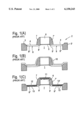
- reference numeral 1 indicates a portion of a silicon-containing semiconductor substrate of a first conductivity type (p or n), fabricated as a MOS transistor precursor 2 for use in a salicide process scheme.
- Precursor 2 is processed, as by conventional techniques not described here in detail in order to not unnecessarily obscure the primary significance of the following description.
- Precursor 2 comprises a plurality of, illustratively two, isolation regions 3 and 3' of a silicon oxide extending from the substrate surface 4 to a prescribed depth below the surface.
- LDDs very shallow and lightly doped first regions
- a layer 10 of a refractory metal is formed, as by DC sputtering, to cover the exposed upper surfaces of the precursor 2.
- Suitable thicknesses of layer 10 are chosen according to the particular metal (due to the above-mentioned differences in silicon consumption ratios) and the junction depth of the second source and drain regions 8" and 9".
- Typical thicknesses of layer 10 range from about 70 ⁇ to about 200 ⁇ for junction depths from about 800 ⁇ to about 3000 ⁇ .
- a thermal treatment typically rapid thermal annealing (RTA) is performed at a temperature and for a time sufficient to convert metal layer 10 to the corresponding electrically conductive metal silicide, e.g., CoSi 2 , NiSi 2 , or TiSi 2 .
- RTA rapid thermal annealing
- Typical RTA conditions for forming CoSi 2 in a two-phase process may be as previously described. Since the refractory metal silicide forms only where metal layer 10 is in contact with underlying silicon, the unreacted portions of metal layer 10 formed over the silicon oxide isolation regions 3, 3' and silicon nitride sidewall spacers 7, 7' are selectively removed, as by a wet etch process.
- the resulting structure after reaction and removal of unreacted metal comprises metal silicide layer portions 11 and 12, 12' respectively formed over gate electrode 6 and source and drain second, heavily doped regions 8" and 9".
- the lower surfaces of the metal silicide layer portions are rough at the silicide-silicon interfaces, resulting in penetration of the underlying silicon substrate by the silicide.
- Such penetration of the silicon in the region below the source and drain second regions 8" and 9", illustratively shown at 13, can cause local shorting of the junction, thereby resulting in junction leakage.
- the effect of penetration is greatest with metals such as cobalt, which have relatively high silicon consumption ratios.
- junction penetration can be avoided or at least minimized and junction integrity provided by increasing the junction depth of the source and drain second regions 8", 9" or by providing a thinner refractory metal layer, thereby reducing silicon consumption.
- the former approach runs counter to the trend toward smaller device dimensions, both vertically and laterally, in order to increase switching speeds, and the latter approach results in an increase in metal silicide sheet resistance attendant its decrease in thickness.
- An advantage of the present invention is a method of manufacturing a high density integrated semiconductor device with an improved self-aligned contact structure.
- Another advantage of the present invention is a method of forming CMOS and similar type devices and transistors with metal silicide-contacted, ultra-shallow source and drain regions having conformal junction layers exhibiting very low junction leakage.
- Still another advantage of the present invention is a method of forming a low sheet resistance, self-contacted ultra-shallow junction in a silicon containing substrate.
- Yet another advantage of the present invention is a MOS transistor having very low sheet resistance self-aligned salicide contacts and ultra-shallow, conformal source and drain junction regions with very low junction leakage.
- a method of manufacturing a semiconductor device which method comprises:
- a refractory metal layer on a surface of a first conductivity type region of a silicon-containing semiconductor substrate, this metal layer being capped or uncapped;
- the thin doped layer of second conductivity type forming an ultra-shallow depth junction with the first conductivity type region of the substrate and the metal silicide layer forming a self-aligned, low sheet resistance ohmic contact to the thin doped layer.
- the semiconductor device comprises a self-aligned MOS transistor and the silicon-containing semiconductor substrate comprises a MOS transistor precursor comprising:
- a pair of spaced apart, shallow depth, lightly doped source and drain regions of a second, opposite conductivity type formed in the substrate surface between the isolation regions and each extending to a proximal edge of a respective isolation region;
- a patterned, thin gate insulating layer formed on the substrate surface between and extending to respective proximal edges of the source and drain regions;
- a gate electrode in overlying contact with the gate insulating layer, the gate electrode comprising opposing side surfaces and a top surface;
- insulative sidewall spacers formed on the side surfaces of the gate electrode and covering underlying portions of the lightly doped, shallow depth source and drain regions;
- said method comprising:
- the thin, heavily doped second conductivity type layers (a) forming ultra-shallow depth, heavily doped source and drain regions in the first conductivity type silicon-containing substrate; (b) extending into touching contact with the shallow depth, lightly doped source and drain regions underlying the sidewall spacers; (c) being self-aligned to the metal silicide-silicon interface; (d) having a substantially constant thickness; and (e) conforming to variations in the irregular lower surface contour of the overlying metal silicide layer portions.
- the isolation regions each comprise a silicon oxide; the thin gate insulating layer comprises a silicon oxide; the gate electrode comprises polysilicon; the sidewall spacers each comprise a silicon nitride or silicon oxynitride; the metal layer comprises a cobalt metal layer, the metal silicide layer comprises a cobalt silicide layer, the dielectric layer comprises a silicon oxide layer, the dopant impurities comprise boron containing ions or phosphorus or arsenic containing ions; and the ions are implanted under conditions selected such that they are implanted only into the dielectric layer and no metal from the metal silicide layer is secondarily implanted into the underlying silicon of the substrate.
- FIGS. 1(A)-1(C) are simplified, cross-sectional schematic diagrams illustrating process steps for forming salicide contacts to the source and drain region of a MOS transistor, according to conventional processing technology.
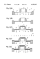
- FIGS. 2(A)-2(E) are simplified, cross sectional schematic diagrams illustrating process steps for forming salicide contacts to the source and drain regions of a MOS transistor, in accordance with an embodiment of the present invention.
- Precursor 2' differs from that shown in FIG. 1(A) in that source and drain regions 8 and 9 formed therein or thereon comprise lightly doped (i.e.
- region I is of n-type conductivity
- region 1 is of p-type conductivity
- CMOS devices will, of course, comprise both n- and p-type regions 1 formed in the substrate in spaced apart array.
- a layer 10 of a refractory metal typically cobalt, nickel or titanium, preferably cobalt, is formed to cover the exposed upper surfaces of precursor 2', in a fashion completely analogous to that of the conventional art shown and described with respect to FIG. 1(B).
- layer 10 is then subjected to a rapid thermal annealing process (RTA) to convert portions thereof in contact with underlying silicon to an electrically conductive metal silicide.
- RTA rapid thermal annealing process
- RTA is preferably performed according to a two-phase process as described above
- FIG. 2(C) shows the result after RTA and removal of unreacted portions of the refractory metal layer 10.
- the portions 8", 9" (sometimes referred to as “extensions") of the lightly doped, shallow source/drain regions 9 in underlying contact with the refractory metal layer 10 are consumed during the silicidization reaction effected by the RTA process, leaving lightly doped source/drain (LDD) regions 8' and 9' beneath respective sidewall spacers 7 and 7'.
- LDD lightly doped source/drain
- CoSi 2 layers of thickness from about 250 ⁇ to about 730 ⁇ and sheet resistance from about 10 ohms/square to about 3 ohms/square are formed as a result of two-phase silicidization reaction performed as described above.
- the lower surfaces 14 of the metal silicide layer portions 11 and 12, 12' are irregular at their respective interfaces with underlying silicon of substrate 1.
- a layer 15 of a dielectric material e.g., a silicon oxide, silicon nitride, or silicon oxynitride
- a source/drain implantation process performed under conditions such that no metal (e.g., cobalt) from the metal silicide (e.g., CoSi 2 ) layer portions is secondarily implanted into the underlying silicon of substrate 1 by momentum transfer ("knock-on").
- no metal e.g., cobalt
- CoSi 2 metal silicide
- Prevention of such secondary implantation is necessary to avoid metal-induced junction leakage.
- boron-containing p-type dopant ions 16 are implanted at a dosage from about 1 ⁇ 10 15 da/cm 2 to about 1 ⁇ 10 16 da/cm 2 at an implantation energy from about 10 keV to about 100 keV.
- phosphorus- or arsenic- containing n-type dopant ions 16 are implanted at a dosage from about 1 ⁇ 10 15 da/cm 2 to about 1 ⁇ 10 16 da/cm 2 at an implantation energy from about 10 keV to about 100 keV.
- the ion-implanted dielectric layer 15 is then subjected to a low temperature annealing for out-diffusion of the implanted dopant to form ultra-shallow source/drain junction regions 17, 17' of average depth below the respective metal silicide layer portion 12, 12' from about 50 ⁇ to about 500 ⁇ and in touching contact (at 18, 18') with lightly doped source/drain regions (LDDs) 8', 9'.
- LDDs lightly doped source/drain regions
- low temperature thermal treatment for out-diffusion of the implanted ions comprises heating at a temperature from about 750° C. to about 900° C. for from about 60 sec to about 600 sec.
- heavily-doped junction regions 17, 17' of dopant concentration from about 8 ⁇ 10 19 da/cm 3 to about 4 ⁇ 10 20 da/cm 3 form very close to, e.g., within about 50 ⁇ to about 500 ⁇ , preferably about 300 ⁇ , of the CoSi 2 /Si interface, following any given interface roughness or contour.
- junction integrity can be maintained even for very shallow, heavily-doped junctions such as herein contemplated, avoiding the risk of high level junction leakage by silicide-induced local short circuits as in the conventional art.
- silicide optimization for low sheet resistance and junction integrity can be de-coupled, advantageously introducing an additional degree of freedom in CMOS device engineering.
- the present invention provides several technological advantages over existing methodology, including, but not limited to, formation of self-aligned, ultra-shallow, heavily-doped source and drain junction regions, which junction regions avoid junction leakage normally associated with formation of overlying low sheet resistance metal silicide contacts thereto.
- the inventive method is easily compatible with conventional process methodology and permits an additional degree of freedom in fabricating low sheet resistance salicide contacts to ultra-shallow source/drain regions.
Abstract
Description
Claims (19)
Priority Applications (1)
| Application Number | Priority Date | Filing Date | Title |
|---|---|---|---|
| US09/186,065 US6150243A (en) | 1998-11-05 | 1998-11-05 | Shallow junction formation by out-diffusion from a doped dielectric layer through a salicide layer |
Applications Claiming Priority (1)
| Application Number | Priority Date | Filing Date | Title |
|---|---|---|---|
| US09/186,065 US6150243A (en) | 1998-11-05 | 1998-11-05 | Shallow junction formation by out-diffusion from a doped dielectric layer through a salicide layer |
Publications (1)
| Publication Number | Publication Date |
|---|---|
| US6150243A true US6150243A (en) | 2000-11-21 |
Family
ID=22683517
Family Applications (1)
| Application Number | Title | Priority Date | Filing Date |
|---|---|---|---|
| US09/186,065 Expired - Lifetime US6150243A (en) | 1998-11-05 | 1998-11-05 | Shallow junction formation by out-diffusion from a doped dielectric layer through a salicide layer |
Country Status (1)
| Country | Link |
|---|---|
| US (1) | US6150243A (en) |
Cited By (28)
| Publication number | Priority date | Publication date | Assignee | Title |
|---|---|---|---|---|
| US6297148B1 (en) * | 1999-08-19 | 2001-10-02 | Advanced Micro Devices, Inc. | Method of forming a silicon bottom anti-reflective coating with reduced junction leakage during salicidation |
| US6339005B1 (en) * | 1999-10-22 | 2002-01-15 | International Business Machines Corporation | Disposable spacer for symmetric and asymmetric Schottky contact to SOI MOSFET |
| US6376342B1 (en) * | 2000-09-27 | 2002-04-23 | Vanguard International Semiconductor Corporation | Method of forming a metal silicide layer on a source/drain region of a MOSFET device |
| US6380057B1 (en) * | 2001-02-13 | 2002-04-30 | Advanced Micro Devices, Inc. | Enhancement of nickel silicide formation by use of nickel pre-amorphizing implant |
| US6518107B2 (en) * | 2001-02-16 | 2003-02-11 | Advanced Micro Devices, Inc. | Non-arsenic N-type dopant implantation for improved source/drain interfaces with nickel silicides |
| US6573160B2 (en) * | 2000-05-26 | 2003-06-03 | Motorola, Inc. | Method of recrystallizing an amorphous region of a semiconductor |
| US6589836B1 (en) * | 2002-10-03 | 2003-07-08 | Taiwan Semiconductor Manufacturing Company | One step dual salicide formation for ultra shallow junction applications |
| US20040198032A1 (en) * | 2001-03-19 | 2004-10-07 | Samsung Electronics Co., Ltd. | Semiconductor device having silicide thin film and method of forming the same |
| US6812523B1 (en) | 2001-09-21 | 2004-11-02 | Wei-Kan Chu | Semiconductor wafer with ultra thin doping level formed by defect engineering |
| US20040224488A1 (en) * | 2002-11-19 | 2004-11-11 | Silterra Malaysia Sdn. Bhd. | Method of forming ultra shallow junctions |
| US20050074932A1 (en) * | 2003-10-03 | 2005-04-07 | Chuan-Yi Lin | Dual fully-silicided gate mosfets |
| US20060189167A1 (en) * | 2005-02-18 | 2006-08-24 | Hsiang-Ying Wang | Method for fabricating silicon nitride film |
| KR100678311B1 (en) * | 2001-12-28 | 2007-02-01 | 매그나칩 반도체 유한회사 | Method of manufacturing a transistor in a semiconductor device |
| US20070170508A1 (en) * | 2003-12-29 | 2007-07-26 | Samsung Electronics Co., Ltd. | Semiconductor device and method of manufacturing the semiconductor device |
| US20070249131A1 (en) * | 2006-04-21 | 2007-10-25 | International Business Machines Corporation | Opto-thermal annealing methods for forming metal gate and fully silicided gate field effect transistors |
| US20090325357A1 (en) * | 2006-06-21 | 2009-12-31 | Kabushiki Kaisha Toshiba | Semiconductor device and method of manufacturing the same |
| US20100109099A1 (en) * | 2008-10-30 | 2010-05-06 | Kabushiki Kaisha Toshiba | Semiconductor device and manufacturing method thereof |
| US20110027958A1 (en) * | 2006-06-26 | 2011-02-03 | Taiwan Semiconductor Manufacturing Company, Ltd. | Methods of Forming Silicide Regions and Resulting MOS Devices |
| US20120139047A1 (en) * | 2010-11-29 | 2012-06-07 | Jun Luo | Semiconductor device and method of manufacturing the same |
| US8450208B2 (en) | 2010-09-29 | 2013-05-28 | Kabushiki Kaisha Toshiba | Semiconductor device manufacturing method |
| US8569158B2 (en) | 2011-03-31 | 2013-10-29 | Tokyo Electron Limited | Method for forming ultra-shallow doping regions by solid phase diffusion |
| US8580664B2 (en) | 2011-03-31 | 2013-11-12 | Tokyo Electron Limited | Method for forming ultra-shallow boron doping regions by solid phase diffusion |
| US8642433B2 (en) * | 2011-08-17 | 2014-02-04 | Institute of Microelectronics, Academy of Sciences | Method for manufacturing semiconductor device |
| US9899224B2 (en) | 2015-03-03 | 2018-02-20 | Tokyo Electron Limited | Method of controlling solid phase diffusion of boron dopants to form ultra-shallow doping regions |
| US10304938B2 (en) | 2016-09-01 | 2019-05-28 | International Business Machines Corporation | Maskless method to reduce source-drain contact resistance in CMOS devices |
| CN109830430A (en) * | 2019-01-29 | 2019-05-31 | 广东工业大学 | A kind of silicon nano hole structure and its preparation method and application that distribution area is controllable |
| CN111129143A (en) * | 2018-10-31 | 2020-05-08 | 台湾积体电路制造股份有限公司 | Semiconductor device and method of forming the same |
| US11322363B2 (en) * | 2019-06-05 | 2022-05-03 | Stmicroelectronics (Crolles 2) Sas | Contacts for electronic component |
Citations (11)
| Publication number | Priority date | Publication date | Assignee | Title |
|---|---|---|---|---|
| US4835112A (en) * | 1988-03-08 | 1989-05-30 | Motorola, Inc. | CMOS salicide process using germanium implantation |
| US5118639A (en) * | 1990-05-29 | 1992-06-02 | Motorola, Inc. | Process for the formation of elevated source and drain structures in a semiconductor device |
| US5208472A (en) * | 1988-05-13 | 1993-05-04 | Industrial Technology Research Institute | Double spacer salicide MOS device and method |
| US5536684A (en) * | 1994-06-30 | 1996-07-16 | Intel Corporation | Process for formation of epitaxial cobalt silicide and shallow junction of silicon |
| US5569624A (en) * | 1995-06-05 | 1996-10-29 | Regents Of The University Of California | Method for shallow junction formation |
| US5646435A (en) * | 1995-04-04 | 1997-07-08 | Taiwan Semiconductor Manufacturing Company, Ltd. | Method for fabricating CMOS field effect transistors having sub-quarter micrometer channel lengths with improved short channel effect characteristics |
| US5691225A (en) * | 1995-10-31 | 1997-11-25 | Nec Corporation | Method for fabricating semiconductor device having CMOS structure |
| US5691212A (en) * | 1996-09-27 | 1997-11-25 | Taiwan Semiconductor Manufacturing Company, Ltd. | MOS device structure and integration method |
| US5731239A (en) * | 1997-01-22 | 1998-03-24 | Chartered Semiconductor Manufacturing Pte Ltd. | Method of making self-aligned silicide narrow gate electrodes for field effect transistors having low sheet resistance |
| US5827760A (en) * | 1996-02-12 | 1998-10-27 | Lg Electronics Inc. | Method for fabricating a thin film transistor of a liquid crystal display device |
| US5926715A (en) * | 1997-06-04 | 1999-07-20 | Mosel Vitelic Inc. | Method of forming lightly-doped drain by automatic PSG doping |
-
1998
- 1998-11-05 US US09/186,065 patent/US6150243A/en not_active Expired - Lifetime
Patent Citations (11)
| Publication number | Priority date | Publication date | Assignee | Title |
|---|---|---|---|---|
| US4835112A (en) * | 1988-03-08 | 1989-05-30 | Motorola, Inc. | CMOS salicide process using germanium implantation |
| US5208472A (en) * | 1988-05-13 | 1993-05-04 | Industrial Technology Research Institute | Double spacer salicide MOS device and method |
| US5118639A (en) * | 1990-05-29 | 1992-06-02 | Motorola, Inc. | Process for the formation of elevated source and drain structures in a semiconductor device |
| US5536684A (en) * | 1994-06-30 | 1996-07-16 | Intel Corporation | Process for formation of epitaxial cobalt silicide and shallow junction of silicon |
| US5646435A (en) * | 1995-04-04 | 1997-07-08 | Taiwan Semiconductor Manufacturing Company, Ltd. | Method for fabricating CMOS field effect transistors having sub-quarter micrometer channel lengths with improved short channel effect characteristics |
| US5569624A (en) * | 1995-06-05 | 1996-10-29 | Regents Of The University Of California | Method for shallow junction formation |
| US5691225A (en) * | 1995-10-31 | 1997-11-25 | Nec Corporation | Method for fabricating semiconductor device having CMOS structure |
| US5827760A (en) * | 1996-02-12 | 1998-10-27 | Lg Electronics Inc. | Method for fabricating a thin film transistor of a liquid crystal display device |
| US5691212A (en) * | 1996-09-27 | 1997-11-25 | Taiwan Semiconductor Manufacturing Company, Ltd. | MOS device structure and integration method |
| US5731239A (en) * | 1997-01-22 | 1998-03-24 | Chartered Semiconductor Manufacturing Pte Ltd. | Method of making self-aligned silicide narrow gate electrodes for field effect transistors having low sheet resistance |
| US5926715A (en) * | 1997-06-04 | 1999-07-20 | Mosel Vitelic Inc. | Method of forming lightly-doped drain by automatic PSG doping |
Non-Patent Citations (6)
| Title |
|---|
| "Ultra Shallow Junction Formation Using Diffusion from Silicides" H. Jiang et al., H. Electrochem. Soc., vol. 139, No. 1, Jan. 1992, pp. 196-218. |
| Materials and Bulk Processes, "Doping Technologies", The National Technology Roadmap for Semiconductors (1994), pp. 118-121. |
| Materials and Bulk Processes, Doping Technologies , The National Technology Roadmap for Semiconductors (1994), pp. 118 121. * |
| S.Wolf and R. Tauber, "Silicon Processing for the VLSI Era", vol. 1, Process Technology, pp. 264-267, 323-327, 1986. |
| S.Wolf and R. Tauber, Silicon Processing for the VLSI Era , vol. 1, Process Technology, pp. 264 267, 323 327, 1986. * |
| Ultra Shallow Junction Formation Using Diffusion from Silicides H. Jiang et al., H. Electrochem. Soc., vol. 139, No. 1, Jan. 1992, pp. 196 218. * |
Cited By (45)
| Publication number | Priority date | Publication date | Assignee | Title |
|---|---|---|---|---|
| US6297148B1 (en) * | 1999-08-19 | 2001-10-02 | Advanced Micro Devices, Inc. | Method of forming a silicon bottom anti-reflective coating with reduced junction leakage during salicidation |
| US7183573B2 (en) | 1999-10-22 | 2007-02-27 | International Business Machines Corporation | Disposable spacer for symmetric and asymmetric Schottky contact to SOI mosfet |
| US6339005B1 (en) * | 1999-10-22 | 2002-01-15 | International Business Machines Corporation | Disposable spacer for symmetric and asymmetric Schottky contact to SOI MOSFET |
| US6573160B2 (en) * | 2000-05-26 | 2003-06-03 | Motorola, Inc. | Method of recrystallizing an amorphous region of a semiconductor |
| US6376342B1 (en) * | 2000-09-27 | 2002-04-23 | Vanguard International Semiconductor Corporation | Method of forming a metal silicide layer on a source/drain region of a MOSFET device |
| US6380057B1 (en) * | 2001-02-13 | 2002-04-30 | Advanced Micro Devices, Inc. | Enhancement of nickel silicide formation by use of nickel pre-amorphizing implant |
| US6518107B2 (en) * | 2001-02-16 | 2003-02-11 | Advanced Micro Devices, Inc. | Non-arsenic N-type dopant implantation for improved source/drain interfaces with nickel silicides |
| US20040198032A1 (en) * | 2001-03-19 | 2004-10-07 | Samsung Electronics Co., Ltd. | Semiconductor device having silicide thin film and method of forming the same |
| US7385260B2 (en) * | 2001-03-19 | 2008-06-10 | Samsung Electronics Co., Ltd. | Semiconductor device having silicide thin film and method of forming the same |
| US6812523B1 (en) | 2001-09-21 | 2004-11-02 | Wei-Kan Chu | Semiconductor wafer with ultra thin doping level formed by defect engineering |
| KR100678311B1 (en) * | 2001-12-28 | 2007-02-01 | 매그나칩 반도체 유한회사 | Method of manufacturing a transistor in a semiconductor device |
| US6589836B1 (en) * | 2002-10-03 | 2003-07-08 | Taiwan Semiconductor Manufacturing Company | One step dual salicide formation for ultra shallow junction applications |
| US7022577B2 (en) * | 2002-11-19 | 2006-04-04 | Silterra Malaysia Sdn. Bhd. | Method of forming ultra shallow junctions |
| US20040224488A1 (en) * | 2002-11-19 | 2004-11-11 | Silterra Malaysia Sdn. Bhd. | Method of forming ultra shallow junctions |
| US6905922B2 (en) * | 2003-10-03 | 2005-06-14 | Taiwan Semiconductor Manufacturing Company, Ltd. | Dual fully-silicided gate MOSFETs |
| US20050074932A1 (en) * | 2003-10-03 | 2005-04-07 | Chuan-Yi Lin | Dual fully-silicided gate mosfets |
| US20070170508A1 (en) * | 2003-12-29 | 2007-07-26 | Samsung Electronics Co., Ltd. | Semiconductor device and method of manufacturing the semiconductor device |
| US20060189167A1 (en) * | 2005-02-18 | 2006-08-24 | Hsiang-Ying Wang | Method for fabricating silicon nitride film |
| US20070249131A1 (en) * | 2006-04-21 | 2007-10-25 | International Business Machines Corporation | Opto-thermal annealing methods for forming metal gate and fully silicided gate field effect transistors |
| US7410852B2 (en) * | 2006-04-21 | 2008-08-12 | International Business Machines Corporation | Opto-thermal annealing methods for forming metal gate and fully silicided gate field effect transistors |
| US8039331B2 (en) | 2006-04-21 | 2011-10-18 | International Business Machines Corporation | Opto-thermal annealing methods for forming metal gate and fully silicided gate-field effect transistors |
| US20090325357A1 (en) * | 2006-06-21 | 2009-12-31 | Kabushiki Kaisha Toshiba | Semiconductor device and method of manufacturing the same |
| US8343870B2 (en) * | 2006-06-21 | 2013-01-01 | Kabushiki Kaisha Toshiba | Semiconductor device and method of manufacturing the same |
| US20110027958A1 (en) * | 2006-06-26 | 2011-02-03 | Taiwan Semiconductor Manufacturing Company, Ltd. | Methods of Forming Silicide Regions and Resulting MOS Devices |
| US8841192B2 (en) | 2006-06-26 | 2014-09-23 | Taiwan Semiconductor Manufacturing Company, Ltd. | Methods of forming silicide regions and resulting MOS devices |
| US9947758B2 (en) | 2006-06-26 | 2018-04-17 | Taiwan Semiconductor Manufacturing Company, Ltd. | Forming silicide regions and resulting MOS devices |
| US9899494B2 (en) | 2006-06-26 | 2018-02-20 | Taiwan Semiconductor Manufacturing Company, Ltd. | Methods of forming silicide regions and resulting MOS devices |
| US8173540B2 (en) | 2006-06-26 | 2012-05-08 | Taiwan Semiconductor Manufacturing Co., Ltd. | Methods of forming silicide regions and resulting MOS devices |
| US20100109099A1 (en) * | 2008-10-30 | 2010-05-06 | Kabushiki Kaisha Toshiba | Semiconductor device and manufacturing method thereof |
| US8816448B2 (en) | 2008-10-30 | 2014-08-26 | Kabushiki Kaisha Toshiba | Semiconductor device and manufacturing method thereof |
| US8450208B2 (en) | 2010-09-29 | 2013-05-28 | Kabushiki Kaisha Toshiba | Semiconductor device manufacturing method |
| US20120139047A1 (en) * | 2010-11-29 | 2012-06-07 | Jun Luo | Semiconductor device and method of manufacturing the same |
| US9012316B2 (en) | 2011-03-31 | 2015-04-21 | Tokyo Electron Limited | Method for forming ultra-shallow boron doping regions by solid phase diffusion |
| US8877620B2 (en) | 2011-03-31 | 2014-11-04 | Tokyo Electron Limited | Method for forming ultra-shallow doping regions by solid phase diffusion |
| US8580664B2 (en) | 2011-03-31 | 2013-11-12 | Tokyo Electron Limited | Method for forming ultra-shallow boron doping regions by solid phase diffusion |
| US8569158B2 (en) | 2011-03-31 | 2013-10-29 | Tokyo Electron Limited | Method for forming ultra-shallow doping regions by solid phase diffusion |
| US8642433B2 (en) * | 2011-08-17 | 2014-02-04 | Institute of Microelectronics, Academy of Sciences | Method for manufacturing semiconductor device |
| US9899224B2 (en) | 2015-03-03 | 2018-02-20 | Tokyo Electron Limited | Method of controlling solid phase diffusion of boron dopants to form ultra-shallow doping regions |
| US10304938B2 (en) | 2016-09-01 | 2019-05-28 | International Business Machines Corporation | Maskless method to reduce source-drain contact resistance in CMOS devices |
| CN111129143A (en) * | 2018-10-31 | 2020-05-08 | 台湾积体电路制造股份有限公司 | Semiconductor device and method of forming the same |
| US11626518B2 (en) | 2018-10-31 | 2023-04-11 | Taiwan Semiconductor Manufacturing Company, Ltd. | FinFET device and methods of forming the same |
| CN111129143B (en) * | 2018-10-31 | 2023-08-22 | 台湾积体电路制造股份有限公司 | Semiconductor device and method of forming the same |
| CN109830430A (en) * | 2019-01-29 | 2019-05-31 | 广东工业大学 | A kind of silicon nano hole structure and its preparation method and application that distribution area is controllable |
| CN109830430B (en) * | 2019-01-29 | 2021-04-23 | 广东工业大学 | Silicon nanopore structure with controllable distribution area and preparation method and application thereof |
| US11322363B2 (en) * | 2019-06-05 | 2022-05-03 | Stmicroelectronics (Crolles 2) Sas | Contacts for electronic component |
Similar Documents
| Publication | Publication Date | Title |
|---|---|---|
| US6150243A (en) | Shallow junction formation by out-diffusion from a doped dielectric layer through a salicide layer | |
| US5496750A (en) | Elevated source/drain junction metal oxide semiconductor field-effect transistor using blanket silicon deposition | |
| US6072222A (en) | Silicon implantation into selective areas of a refractory metal to reduce consumption of silicon-based junctions during salicide formation | |
| US5322809A (en) | Self-aligned silicide process | |
| US7098514B2 (en) | Highly integrated semiconductor device with silicide layer that secures contact margin and method of manufacturing the same | |
| US6617654B2 (en) | Semiconductor device with sidewall spacers and elevated source/drain region | |
| US6630721B1 (en) | Polysilicon sidewall with silicide formation to produce high performance MOSFETS | |
| JPH08148561A (en) | Semiconductor device and its manufacture | |
| US6461951B1 (en) | Method of forming a sidewall spacer to prevent gouging of device junctions during interlayer dielectric etching including silicide growth over gate spacers | |
| US5918130A (en) | Transistor fabrication employing formation of silicide across source and drain regions prior to formation of the gate conductor | |
| US6271133B1 (en) | Optimized Co/Ti-salicide scheme for shallow junction deep sub-micron device fabrication | |
| US6015753A (en) | Method of forming a self-aligned silicide | |
| US6451679B1 (en) | Ion mixing between two-step titanium deposition process for titanium salicide CMOS technology | |
| US6461923B1 (en) | Sidewall spacer etch process for improved silicide formation | |
| US6165857A (en) | Method for forming a transistor with selective epitaxial growth film | |
| US6096647A (en) | Method to form CoSi2 on shallow junction by Si implantation | |
| US6518107B2 (en) | Non-arsenic N-type dopant implantation for improved source/drain interfaces with nickel silicides | |
| KR100568077B1 (en) | Method for manufacturing semiconductor device | |
| US6368949B1 (en) | Post-spacer etch surface treatment for improved silicide formation | |
| KR100835521B1 (en) | Structrue of semiconcuctor device and method of menufacturing the same | |
| US5858846A (en) | Salicide integration method | |
| US6258682B1 (en) | Method of making ultra shallow junction MOSFET | |
| US6204136B1 (en) | Post-spacer etch surface treatment for improved silicide formation | |
| US6171919B1 (en) | MOS Transistor formation process including post-spacer etch surface treatment for improved silicide formation | |
| US6162689A (en) | Multi-depth junction formation tailored to silicide formation |
Legal Events
| Date | Code | Title | Description |
|---|---|---|---|
| AS | Assignment |
Owner name: ADVANCED MICRO DEVICES, INC., CALIFORNIA Free format text: ASSIGNMENT OF ASSIGNORS INTEREST;ASSIGNORS:WIECZOREK, KARSTEN;KEPLER, NICK;WANG, LARRY;AND OTHERS;REEL/FRAME:009573/0510;SIGNING DATES FROM 19980923 TO 19981008 |
|
| STCF | Information on status: patent grant |
Free format text: PATENTED CASE |
|
| FPAY | Fee payment |
Year of fee payment: 4 |
|
| FPAY | Fee payment |
Year of fee payment: 8 |
|
| AS | Assignment |
Owner name: GLOBALFOUNDRIES INC., CAYMAN ISLANDS Free format text: AFFIRMATION OF PATENT ASSIGNMENT;ASSIGNOR:ADVANCED MICRO DEVICES, INC.;REEL/FRAME:023119/0083 Effective date: 20090630 |
|
| FPAY | Fee payment |
Year of fee payment: 12 |
|
| AS | Assignment |
Owner name: WILMINGTON TRUST, NATIONAL ASSOCIATION, DELAWARE Free format text: SECURITY AGREEMENT;ASSIGNOR:GLOBALFOUNDRIES INC.;REEL/FRAME:049490/0001 Effective date: 20181127 |
|
| AS | Assignment |
Owner name: GLOBALFOUNDRIES INC., CAYMAN ISLANDS Free format text: RELEASE BY SECURED PARTY;ASSIGNOR:WILMINGTON TRUST, NATIONAL ASSOCIATION;REEL/FRAME:054636/0001 Effective date: 20201117 |
|
| AS | Assignment |
Owner name: GLOBALFOUNDRIES U.S. INC., NEW YORK Free format text: RELEASE BY SECURED PARTY;ASSIGNOR:WILMINGTON TRUST, NATIONAL ASSOCIATION;REEL/FRAME:056987/0001 Effective date: 20201117 |