US6148426A - Apparatus and method for generating addresses in a SRAM built-in self test circuit using a single-direction counter - Google Patents
Apparatus and method for generating addresses in a SRAM built-in self test circuit using a single-direction counter Download PDFInfo
- Publication number
- US6148426A US6148426A US09/067,671 US6767198A US6148426A US 6148426 A US6148426 A US 6148426A US 6767198 A US6767198 A US 6767198A US 6148426 A US6148426 A US 6148426A
- Authority
- US
- United States
- Prior art keywords
- address
- memory
- addresses
- series
- bist
- Prior art date
- Legal status (The legal status is an assumption and is not a legal conclusion. Google has not performed a legal analysis and makes no representation as to the accuracy of the status listed.)
- Expired - Lifetime
Links
Images
Classifications
-
- G—PHYSICS
- G11—INFORMATION STORAGE
- G11C—STATIC STORES
- G11C29/00—Checking stores for correct operation ; Subsequent repair; Testing stores during standby or offline operation
- G11C29/04—Detection or location of defective memory elements, e.g. cell constructio details, timing of test signals
- G11C29/08—Functional testing, e.g. testing during refresh, power-on self testing [POST] or distributed testing
- G11C29/12—Built-in arrangements for testing, e.g. built-in self testing [BIST] or interconnection details
- G11C29/18—Address generation devices; Devices for accessing memories, e.g. details of addressing circuits
- G11C29/20—Address generation devices; Devices for accessing memories, e.g. details of addressing circuits using counters or linear-feedback shift registers [LFSR]
-
- G—PHYSICS
- G01—MEASURING; TESTING
- G01R—MEASURING ELECTRIC VARIABLES; MEASURING MAGNETIC VARIABLES
- G01R31/00—Arrangements for testing electric properties; Arrangements for locating electric faults; Arrangements for electrical testing characterised by what is being tested not provided for elsewhere
- G01R31/26—Testing of individual semiconductor devices
-
- G—PHYSICS
- G11—INFORMATION STORAGE
- G11C—STATIC STORES
- G11C29/00—Checking stores for correct operation ; Subsequent repair; Testing stores during standby or offline operation
-
- H—ELECTRICITY
- H10—SEMICONDUCTOR DEVICES; ELECTRIC SOLID-STATE DEVICES NOT OTHERWISE PROVIDED FOR
- H10P—GENERIC PROCESSES OR APPARATUS FOR THE MANUFACTURE OR TREATMENT OF DEVICES COVERED BY CLASS H10
- H10P74/00—Testing or measuring during manufacture or treatment of wafers, substrates or devices
Definitions
- the present invention relates to a SRAM built-in self test (SRAM BIST) circuit, and more particularly, to an address generator and a method of generating an address and an SRAM BIST using the same.
- SRAM BIST SRAM built-in self test
- BIST memory built-in self test
- a SRAM BIST circuit typically includes a BIST controller for controlling BIST operation, a data generator for generating data to be written to the SRAM, an address generator for generating an address for the SRAM, a comparator for comparing data read from the SRAM, and a counter for counting steps of the test process.
- a typical address generator performs both up counting and down counting according to the test procedure.
- the address generator is produced using such an up/down counter, there are difficulties in obtaining an optimized chip area. For example, when the number of addresses in the SRAM to be tested is 2 n , where n is the number of bits in a SRAM memory address, the address generator can be readily realized using the up/down counter; however, the chip area of the address generator is relatively large.
- the number of addresses in the SRAM to be tested is not 2 n and the address generator is realized using the up/down counter, other additional circuitry which interfaces with the up/down counter is required, and the chip area of the address generator becomes even larger.
- the SRAM BIST circuit of the invention includes a BIST controller, a data generator, an address generator, a comparator and a counter.
- the BIST controller generates control signals according to the test process being used and controls the overall BIST circuit operation.
- the data generator is controlled by the BIST controller and generates data to be written in the memory being tested as well as comparison data for comparison to data read from the memory.
- the address generator is controlled by the BIST controller to generate an address of the memory according to the test process.
- the comparator is controlled by the BIST controller and compares the comparison data to the data read from the memory.
- the counter is controlled by the BIST controller to count the steps of the procedure being performed.
- the address generator of a SRAM BIST circuit in accordance with the invention can include an up counter for generating a first series of sequentially increasing addresses and an inverter for inverting the first series of addresses to generate a second series of sequentially decreasing addresses.
- the address generator of the invention in the SRAM BIST circuit of the invention can also include a selector for selecting one or more addresses from the first and/or second series of addresses, in response to an up/down control signal generated by the BIST controller, to output the selected address as a test address of the memory to be tested.
- an address generator of an SRAM BIST circuit in accordance with another aspect of the invention can include an up counter for generating a first series of sequentially increasing addresses up to a maximum address of the memory to be tested and a subtracter for subtracting one or more addresses of the first series of addresses from the maximum address to generate a second series of sequentially decreasing addresses. Also, the address generator of the SRAM BIST circuit of this aspect of the invention further includes a selector for selecting one or more addresses from the first and/or second series of addresses, in response to an up/down control signal generated by the BIST controller, to output the selected address a test address of the memory to be tested.
- a method in accordance with the invention for generating an address of the SRAM BIST circuit for accomplishing the third object includes the steps of generating a first series of sequentially increasing addresses and inverting one or more of the first series of addresses to generate a second series of sequentially decreasing addresses.
- the method for generating an address of the SRAM BIST circuit can also include the step of selecting one or more of the addresses from the first and/or second series of addresses to output the selected address as a test address of the memory to be tested.
- an alternative method in accordance with the invention for generating an address of the SRAM BIST circuit for accomplishing the third object includes the steps of generating a first series of sequentially increasing addresses up to a maximum address of a memory to be tested and subtracting one or more addresses of the first series of addresses from the maximum address to generate a second series of sequentially decreasing addresses.
- the method for generating an address of the SRAM BIST circuit for accomplishing the third object can also include the step of selecting one or more addresses from the first and/or second series of addresses, to output the selected address as an address of the memory to be tested.
- the address generator and BIST circuit of the invention can provide advantages over other such devices. Because the address generator of the invention can use only a single up counter to generate addresses, overall circuit size and complexity can be reduced. Also, the supporting and controlling circuitry can be smaller and less complex, resulting in further savings in size, complexity and cost.
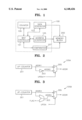
- FIG. 1 is a schematic block diagram of a SRAM BIST circuit in accordance with the present invention
- FIG. 2 is a schematic block diagram of one embodiment of an address generator according to the present invention.
- FIG. 3 is a schematic block diagram of an alternative embodiment of an address generator according to the present invention.
- a SRAM BIST circuit 100 in accordance with the invention used to test a memory block 200 such as a SRAM includes a BIST controller 101, a data generator 103, an address generator 105, a comparator 107 and a counter 109.
- the BIST controller 101 controls the operation of the BIST circuit 100 and generates control signals according to the memory test method being implemented.
- the data generator 103 is controlled by the BIST controller 101 to generate data to be written to the memory block 200 under test (i.e., the SRAM) and to also generate comparison data.
- the comparison data is compared to data written to an addressed location of the memory block 200 to determine whether data can successfully be written to and read from the memory 200.
- the address generator 105 is controlled by the BIST controller 101 to generate the addresses of the locations of the memory block 200 being tested according to the test process of the invention.
- the comparator 107 is controlled by the BIST controller 101 to compare data read from the memory block 200 to the comparison data generated by the data generator.
- the counter 109 is controlled by the BIST controller 101 and counts steps of the test process.
- the address generator 105 of the SRAM BIST circuit 100 performs up- and down-counting according to the memory test procedure.
- the address generator of a BIST circuit is designed using one up/down counter or separate up and down counters. The result is that chip area increases. Accordingly, in the present invention, an address generator 105 having a relatively small chip area and an SRAM BIST circuit 100 using the address generator 105 are provided.
- FIG. 2 is a schematic block diagram of one embodiment of the address generator 105A according to the present invention.
- the embodiment of FIG. 2 is employed when the number of addresses of the memory block 200 of FIG. 1 is 2 n .
- the address generator 105A generates the addresses of the memory block according to a method for generating an address of the present invention.
- the address generator 105A includes one up counter 201, an inverter 203, and a selector 205.
- the up counter 201 generates a first address ADDR1 of a sequentially increasing series of addresses.
- the inverter 203 inverts the first address ADDR1 to generate a second address ADDR2 of a second sequentially decreasing series of addresses.
- the selector 205 selects one from the first and second addresses ADDR1 and ADDR2, in response to the up/down control signal UPDN, to output the selected address as an address ADDR applied to the memory block 200 of FIG. 1 to test the location of the memory block 200 addressed by the address ADDR.
- the selector 205 includes a multiplexer and selects the first address ADDR1 as the address ADDR when the up/down control signal UPDN is logic low and the second address ADDR2 as the address ADDR when the up/down control signal UPDN is logic high.
- the up/down control signal UPDN is generated by the BIST controller 101 of FIG. 1 and has a state determined by a value of a current method step generated by the counter 109.
- Table 1 shows addresses generated by the address generator 105A of FIG. 2.
- the uninverted addresses ADDR1 are counted in ascending or sequentially increasing order.
- the inverted versions of the ADDR1 addresses, labeled ADDR2 are shown in descending or sequentially decreasing order.
- the one of the addresses ADDR1 and ADDR2 that is output from the address generator 105A as the address ADDR is determined by the state of the control signal UPDN.
- FIG. 3 contains a schematic block diagram of another embodiment 105B of an address generator in accordance with the invention.
- the address generator 105B of FIG. 3 is employed when the number of addresses of the memory block 200 of FIG. 1 is not 2 n .
- This embodiment of the address generator 105B uses an approach to generating addresses different than that used by the address generator 105A described above.
- the address generator 105B includes one up counter 301, a subtracter circuit 303 and a selector 305.
- the up counter 301 generates a first address ADDR3 of a sequentially increasing series of addresses to a maximum address of the memory to be tested, i.e., the memory block 200.
- the subtracter 303 subtracts the first address ADDR3 from a flag value FLAG identical to the maximum address, to generate a second address ADDR4 of a sequentially decreasing series of addresses.
- the selector 305 selects one from the first and second addresses ADDR3 and ADDR4, in response to the up/down control signal UPDN, to output the selected address as an address ADDR applied to the memory block 200 of FIG. 1 to test the location of the memory block 200 addressed by the address ADDR.
- the selector 305 includes a multiplexer and selects the first address ADDR3 as the address ADDR when the up/down control signal UPDN is logic low and selects the second address ADDR4 as the address ADDR when the up/down control signal UPDN is logic high.
- the up/down control signal UPDN is generated by the BIST controller 101 of FIG. 1, and has a state determined by the value of a current method step generated by the counter 109.
- Table 2 shows addresses generated by the address generator 105B of FIG. 3.
- the addresses ADDR3 generated by the up counter 301 are counted in ascending or sequentially increasing order.
- Each address ADDR4 is generated by subtracting an address ADDR3 from the FLAG value set to the maximum memory address, which in the illustration is set to a value of 9F H .
- a set of descending or sequentially decreasing addresses ADDR4 is produced.
- the one of the addresses ADDR3 and ADDR4 that is output from the address generator 105B as the address ADDR is determined by the state of the control signal UPDN.
Landscapes
- Physics & Mathematics (AREA)
- General Physics & Mathematics (AREA)
- For Increasing The Reliability Of Semiconductor Memories (AREA)
- Static Random-Access Memory (AREA)
- Tests Of Electronic Circuits (AREA)
Abstract
A memory address generator having a small chip area, a method for generating a memory address and a SRAM built-in self test (BIST) circuit using the same are described. When the number of addresses of a memory to be tested is 2n, where n is the number of bits in an address, the address generator includes an up counter for generating a first address of a series of sequentially increasing addresses, and an inverter for inverting the first address to generate a second address of a series of sequentially decreasing addresses. The address generator also includes a selector for selecting one of the first and second addresses, in response to a control signal, to output the selected address as an address of the memory. When the number of addresses of the memory to be tested is not 2n, the address generator includes an up counter for generating a first address of a series of sequentially increasing addresses up to a maximum address of the memory and a subtracter for subtracting the first address from the maximum address to generate a second address of a series of sequentially decreasing addresses. The address generator also includes a selector for selecting one of the first and second addresses, in response to control signal, to output the selected address as an address of the memory.
Description
1. Field of the Invention
The present invention relates to a SRAM built-in self test (SRAM BIST) circuit, and more particularly, to an address generator and a method of generating an address and an SRAM BIST using the same.
2. Description of the Related Art
In general, as semiconductor devices become more complicated and highly integrated, research is underway on various methods for effectively testing the semiconductor devices. In particular, memory built-in self test (BIST) methods have been developed for effectively testing a memory in a semiconductor device using a BIST circuit implemented in connection with memory test processes.
A SRAM BIST circuit typically includes a BIST controller for controlling BIST operation, a data generator for generating data to be written to the SRAM, an address generator for generating an address for the SRAM, a comparator for comparing data read from the SRAM, and a counter for counting steps of the test process. A typical address generator performs both up counting and down counting according to the test procedure. However, when the address generator is produced using such an up/down counter, there are difficulties in obtaining an optimized chip area. For example, when the number of addresses in the SRAM to be tested is 2n, where n is the number of bits in a SRAM memory address, the address generator can be readily realized using the up/down counter; however, the chip area of the address generator is relatively large. When the number of addresses in the SRAM to be tested is not 2n and the address generator is realized using the up/down counter, other additional circuitry which interfaces with the up/down counter is required, and the chip area of the address generator becomes even larger.
It is a first object of the present invention to provide an address generator occupying a small chip area in a SRAM BIST circuit.
It is a second object of the present invention to provide a SRAM BIST circuit using the address generator of the invention.
It is a third object of the present invention to provide a method for effectively generating an address in a SRAM BIST circuit.
In one embodiment, the SRAM BIST circuit of the invention includes a BIST controller, a data generator, an address generator, a comparator and a counter. The BIST controller generates control signals according to the test process being used and controls the overall BIST circuit operation. The data generator is controlled by the BIST controller and generates data to be written in the memory being tested as well as comparison data for comparison to data read from the memory. The address generator is controlled by the BIST controller to generate an address of the memory according to the test process. The comparator is controlled by the BIST controller and compares the comparison data to the data read from the memory. The counter is controlled by the BIST controller to count the steps of the procedure being performed.
When the number of addresses of a memory to be tested is 2n, where n is the number of bits in a memory address, the address generator of a SRAM BIST circuit in accordance with the invention can include an up counter for generating a first series of sequentially increasing addresses and an inverter for inverting the first series of addresses to generate a second series of sequentially decreasing addresses. The address generator of the invention in the SRAM BIST circuit of the invention can also include a selector for selecting one or more addresses from the first and/or second series of addresses, in response to an up/down control signal generated by the BIST controller, to output the selected address as a test address of the memory to be tested.
When the number of addresses of the memory to be tested is not 2n, an address generator of an SRAM BIST circuit in accordance with another aspect of the invention can include an up counter for generating a first series of sequentially increasing addresses up to a maximum address of the memory to be tested and a subtracter for subtracting one or more addresses of the first series of addresses from the maximum address to generate a second series of sequentially decreasing addresses. Also, the address generator of the SRAM BIST circuit of this aspect of the invention further includes a selector for selecting one or more addresses from the first and/or second series of addresses, in response to an up/down control signal generated by the BIST controller, to output the selected address a test address of the memory to be tested.
Also, when the number of addresses of the memory to be tested is 2n, a method in accordance with the invention for generating an address of the SRAM BIST circuit for accomplishing the third object includes the steps of generating a first series of sequentially increasing addresses and inverting one or more of the first series of addresses to generate a second series of sequentially decreasing addresses. The method for generating an address of the SRAM BIST circuit can also include the step of selecting one or more of the addresses from the first and/or second series of addresses to output the selected address as a test address of the memory to be tested.
When the number of addresses of the memory to be tested is not 2n, an alternative method in accordance with the invention for generating an address of the SRAM BIST circuit for accomplishing the third object includes the steps of generating a first series of sequentially increasing addresses up to a maximum address of a memory to be tested and subtracting one or more addresses of the first series of addresses from the maximum address to generate a second series of sequentially decreasing addresses. The method for generating an address of the SRAM BIST circuit for accomplishing the third object can also include the step of selecting one or more addresses from the first and/or second series of addresses, to output the selected address as an address of the memory to be tested.
Hence, the address generator and BIST circuit of the invention can provide advantages over other such devices. Because the address generator of the invention can use only a single up counter to generate addresses, overall circuit size and complexity can be reduced. Also, the supporting and controlling circuitry can be smaller and less complex, resulting in further savings in size, complexity and cost.
The above objects and advantages of the present invention will become more apparent from the following detailed description of preferred embodiments thereof with reference to the attached drawings in which:
FIG. 1 is a schematic block diagram of a SRAM BIST circuit in accordance with the present invention;
FIG. 2 is a schematic block diagram of one embodiment of an address generator according to the present invention; and
FIG. 3 is a schematic block diagram of an alternative embodiment of an address generator according to the present invention.
Referring to FIG. 1, a SRAM BIST circuit 100 in accordance with the invention used to test a memory block 200 such as a SRAM includes a BIST controller 101, a data generator 103, an address generator 105, a comparator 107 and a counter 109. The BIST controller 101 controls the operation of the BIST circuit 100 and generates control signals according to the memory test method being implemented. The data generator 103 is controlled by the BIST controller 101 to generate data to be written to the memory block 200 under test (i.e., the SRAM) and to also generate comparison data. During test, the comparison data is compared to data written to an addressed location of the memory block 200 to determine whether data can successfully be written to and read from the memory 200. The address generator 105 is controlled by the BIST controller 101 to generate the addresses of the locations of the memory block 200 being tested according to the test process of the invention. The comparator 107 is controlled by the BIST controller 101 to compare data read from the memory block 200 to the comparison data generated by the data generator. The counter 109 is controlled by the BIST controller 101 and counts steps of the test process.
The address generator 105 of the SRAM BIST circuit 100 performs up- and down-counting according to the memory test procedure. In prior systems, the address generator of a BIST circuit is designed using one up/down counter or separate up and down counters. The result is that chip area increases. Accordingly, in the present invention, an address generator 105 having a relatively small chip area and an SRAM BIST circuit 100 using the address generator 105 are provided.
FIG. 2 is a schematic block diagram of one embodiment of the address generator 105A according to the present invention. The embodiment of FIG. 2 is employed when the number of addresses of the memory block 200 of FIG. 1 is 2n. The address generator 105A generates the addresses of the memory block according to a method for generating an address of the present invention.
Referring to FIG. 2, the address generator 105A includes one up counter 201, an inverter 203, and a selector 205. The up counter 201 generates a first address ADDR1 of a sequentially increasing series of addresses. The inverter 203 inverts the first address ADDR1 to generate a second address ADDR2 of a second sequentially decreasing series of addresses. The selector 205 selects one from the first and second addresses ADDR1 and ADDR2, in response to the up/down control signal UPDN, to output the selected address as an address ADDR applied to the memory block 200 of FIG. 1 to test the location of the memory block 200 addressed by the address ADDR.
In one embodiment, the selector 205 includes a multiplexer and selects the first address ADDR1 as the address ADDR when the up/down control signal UPDN is logic low and the second address ADDR2 as the address ADDR when the up/down control signal UPDN is logic high. The up/down control signal UPDN is generated by the BIST controller 101 of FIG. 1 and has a state determined by a value of a current method step generated by the counter 109.
Table 1 shows addresses generated by the address generator 105A of FIG. 2. As shown in Table 1, the uninverted addresses ADDR1 are counted in ascending or sequentially increasing order. The inverted versions of the ADDR1 addresses, labeled ADDR2, are shown in descending or sequentially decreasing order. As shown in Table 1, the one of the addresses ADDR1 and ADDR2 that is output from the address generator 105A as the address ADDR is determined by the state of the control signal UPDN. When UPDN=0, the address ADDR1 is selected to be provided as the output address ADDR, such that the memory can be tested by ascending addresses. When UPDN=1, the address ADDR2 is selected to be provided as the output address ADDR, such that the memory can be tested by descending addresses.
              TABLE 1
______________________________________
                 ADDR
ADDR1    ADDR2         UPDN = 0 UPDN = 1
______________________________________
00000000 11111111      00000000 11111111
00000001 11111110      00000001 11111110
.        .             .        .
.        .             .        .
11111110 00000001      11111110 00000001
11111111 00000000      11111111 00000000
______________________________________
FIG. 3 contains a schematic block diagram of another embodiment 105B of an address generator in accordance with the invention. The address generator 105B of FIG. 3 is employed when the number of addresses of the memory block 200 of FIG. 1 is not 2n. This embodiment of the address generator 105B uses an approach to generating addresses different than that used by the address generator 105A described above.
Referring to FIG. 3, the address generator 105B includes one up counter 301, a subtracter circuit 303 and a selector 305. The up counter 301 generates a first address ADDR3 of a sequentially increasing series of addresses to a maximum address of the memory to be tested, i.e., the memory block 200. The subtracter 303 subtracts the first address ADDR3 from a flag value FLAG identical to the maximum address, to generate a second address ADDR4 of a sequentially decreasing series of addresses. The selector 305 selects one from the first and second addresses ADDR3 and ADDR4, in response to the up/down control signal UPDN, to output the selected address as an address ADDR applied to the memory block 200 of FIG. 1 to test the location of the memory block 200 addressed by the address ADDR.
In one embodiment, the selector 305 includes a multiplexer and selects the first address ADDR3 as the address ADDR when the up/down control signal UPDN is logic low and selects the second address ADDR4 as the address ADDR when the up/down control signal UPDN is logic high. The up/down control signal UPDN is generated by the BIST controller 101 of FIG. 1, and has a state determined by the value of a current method step generated by the counter 109.
Table 2 shows addresses generated by the address generator 105B of FIG. 3. As shown in Table 2, the addresses ADDR3 generated by the up counter 301 are counted in ascending or sequentially increasing order. Each address ADDR4 is generated by subtracting an address ADDR3 from the FLAG value set to the maximum memory address, which in the illustration is set to a value of 9FH. As a result, a set of descending or sequentially decreasing addresses ADDR4 is produced. As shown in Table 2, the one of the addresses ADDR3 and ADDR4 that is output from the address generator 105B as the address ADDR is determined by the state of the control signal UPDN. When UPDN=0, the address ADDR3 is selected to be provided as the output address ADDR, such that the memory can be tested by ascending addresses. When UPDN=1, the address ADDR4 is selected to be provided as the output address ADDR, such that the memory can be tested by descending addresses.
              TABLE 2
______________________________________
                   ADDR
ADDR3    ADDR4    FLAG       UPDN = 0
                                    UPDN = 1
______________________________________
00000000 10011111 10011111   00000000
                                    10011111
00000001 10011110 10011111   00000001
                                    10011110
.        .        .          .      .
.        .        .          .      .
10011110 00000001 10011111   10011110
                                    00000001
10011111 00000000 10011111   10011111
                                    00000000
______________________________________
While this invention has been particularly shown and described with references to preferred embodiments thereof, it will be understood by those skilled in the art that various changes in form and details may be made therein without departing from the spirit and scope of the invention as defined in the following claims.
Claims (20)
1. An address generator of a memory built-in self test (BIST) circuit comprising:
an up counter for generating a series of sequentially increasing addresses;
an inverter for inverting addresses of the series of sequentially increasing addresses to generate a series of sequentially decreasing addresses; and
a selector for selecting one of (i) an address from the series of sequentially increasing addresses and (ii) an address from the series of sequentially decreasing addresses, in response to a control signal, to output the selected address as an address of a memory to be tested.
2. The address generator of claim 1, wherein the selector selects an address from the series of sequentially increasing addresses when the control signal is in a first logic state and selects an address from the series of sequentially decreasing addresses when the control signal is in a second logic state.
3. The address generator of claim 1, wherein the selector is a multiplexer.
4. The address generator of claim 1, wherein the number of addresses of the memory is 2n, where n is the number of bits of an address.
5. An address generator of a memory BIST circuit comprising:
an up counter for generating a first address of a first series of sequentially increasing addresses up to a maximum address of a memory to be tested;
a subtracter for subtracting the first address from the maximum address to generate a second address of a second series of sequentially decreasing addresses; and
a selector for selecting one from the first and second addresses, in response to a control signal, to output the selected address as the address of the memory.
6. The address generator of claim 5, wherein the selector selects the first address when the control signal is in a first logic state and selects the second address when the control signal is in a second logic state.
7. The address generator of claim 5, wherein the selector is a multiplexer.
8. The address generator of claim 5, wherein the number of addresses of the memory is not 2n, where n is the number of bits of an address.
9. A memory built-in self test (BIST) circuit for testing a memory in a semiconductor device, comprising:
a BIST controller for generating control signals according to a test being performed on the memory to control the BIST operation;
a data generator controlled by the BIST controller for generating data to be written to the memory and comparison data for comparing to data read from the memory;
a comparator controlled by the BIST controller for comparing the comparison data with the data read from the memory;
a counter controlled by the BIST controller for counting steps of the test being performed; and
an address generator controlled by the BIST controller for generating the address of the memory according to the test being performed, said address generator comprising:
an up counter for generating a first address of a first series of sequentially increasing addresses;
an inverter for inverting the first address to generate a second address of a second series of sequentially decreasing addresses; and
a selector for selecting one from the first and second addresses, in response to an up/down control signal generated by the BIST controller, to output the selected address as an address of the memory.
10. The memory BIST circuit of claim 9, wherein the selector selects the first address when the up/down control signal is in a first logic state and selects the second address when the up/down control signal is in a second logic state.
11. The memory BIST circuit of claim 9, wherein the selector is a multiplexer.
12. The memory BIST circuit of claim 9, wherein the number of addresses of the memory is 2n, where n is the number of bits of an address.
13. A memory built-in self test (BIST) circuit for testing a memory in a semiconductor device, comprising:
a BIST controller for generating control signals according to a test being performed on the memory to control the BIST operation;
a data generator controlled by the BIST controller for generating data to be written to the memory and comparison data for comparing to data read from the memory;
a comparator controlled by the BIST controller for comparing the comparison data with the data read from the memory;
a counter controlled by the BIST controller for counting steps of the test being performed; and
an address generator controlled by the BIST controller for generating the address of the memory according to the test being performed, said address generator comprising:
an up counter for generating a first address of a first series of sequentially increasing addresses up to a maximum address of the memory;
a subtracter for subtracting the first address from the maximum address to generate a second address of a second series of sequentially decreasing addresses; and
a selector for selecting one from the first and second addresses, in response to an up/down control signal generated by the BIST controller, to output the selected address as an address of the memory.
14. The memory BIST circuit of claim 13, wherein the selector selects the first address when the up/down control signal is in a first logic state and selects the second address when the up/down control signal is in a second logic state.
15. The memory BIST circuit of claim 13, wherein the selector is a multiplexer.
16. The memory BIST circuit of claim 13, wherein the number of addresses of the memory is not 2n, where n is the number of bits of an address.
17. A method for generating an address in a memory BIST circuit comprising:
a) generating a series of sequentially increasing addresses;
b) inverting addresses of the series of sequentially increasing addresses to generate a series of sequentially decreasing addresses; and
c) selecting one of (i) an address from the series of sequentially increasing addresses and (ii) an address from the series of sequentially decreasing addresses to output the selected address as the address of the memory to be tested.
18. The method for generating an address of claim 17, wherein the number of addresses of the memory is 2 n, where n is the number of bits of an address.
19. A method for generating an address in a memory BIST circuit comprising:
a) generating a first address of a first series of sequentially increasing addresses up to a maximum address of a memory to be tested;
b) subtracting the first address from the maximum address to generate a second address of a second series of sequentially decreasing addresses; and
c) selecting one from the first and second addresses to output the selected address as an address of the memory.
20. The method for generating an address of claim 19, wherein the number of addresses of the memory is not 2n, where n is the number of bits of an address.
Applications Claiming Priority (2)
| Application Number | Priority Date | Filing Date | Title |
|---|---|---|---|
| KR97-35208 | 1997-07-25 | ||
| KR1019970035208A KR100468675B1 (en) | 1997-07-25 | 1997-07-25 | Address generator for SRAM BIST and address generating method thereof |
Publications (1)
| Publication Number | Publication Date |
|---|---|
| US6148426A true US6148426A (en) | 2000-11-14 |
Family
ID=19515738
Family Applications (1)
| Application Number | Title | Priority Date | Filing Date |
|---|---|---|---|
| US09/067,671 Expired - Lifetime US6148426A (en) | 1997-07-25 | 1998-04-28 | Apparatus and method for generating addresses in a SRAM built-in self test circuit using a single-direction counter |
Country Status (3)
| Country | Link |
|---|---|
| US (1) | US6148426A (en) |
| JP (1) | JP3735748B2 (en) |
| KR (1) | KR100468675B1 (en) |
Cited By (16)
| Publication number | Priority date | Publication date | Assignee | Title |
|---|---|---|---|---|
| US20030056161A1 (en) * | 2001-09-14 | 2003-03-20 | Christophe Lauga | Memory circuit scan arrangement |
| US6539324B2 (en) * | 2000-07-12 | 2003-03-25 | International Business Machines Corporation | Semiconductor device and semiconductor device testing method |
| US6550023B1 (en) * | 1998-10-19 | 2003-04-15 | Hewlett Packard Development Company, L.P. | On-the-fly memory testing and automatic generation of bitmaps |
| US20030074619A1 (en) * | 2001-10-12 | 2003-04-17 | Dorsey Michael C. | Memory bist employing a memory bist signature |
| US20030074620A1 (en) * | 2001-10-12 | 2003-04-17 | Dorsey Michael C. | Configurable asic memory bist controller employing multiple state machines |
| US20030074616A1 (en) * | 2001-10-12 | 2003-04-17 | Dorsey Michael C. | ASIC BIST controller employing multiple clock domains |
| US20030074618A1 (en) * | 2001-10-12 | 2003-04-17 | Dorsey Michael C. | Dual mode ASIC BIST controller |
| US20030074617A1 (en) * | 2001-10-12 | 2003-04-17 | Dorsey Michael C. | ASIC BIST employing stored indications of completion |
| US20030074614A1 (en) * | 2001-10-12 | 2003-04-17 | Dorsey Michael C. | Utilizing slow ASIC logic BIST to preserve timing integrity across timing domains |
| US20030074621A1 (en) * | 2001-10-12 | 2003-04-17 | Dorsey Michael C. | ASIC logic BIST employing registers seeded with differing primitive polynomials |
| US6668348B1 (en) * | 1999-07-19 | 2003-12-23 | Nec Electronics Corporation | Memory-mounting integrated circuit and test method thereof |
| US6694461B1 (en) * | 1999-07-26 | 2004-02-17 | Ati International Srl | System and method for testing integrated memories |
| US7224638B1 (en) | 2005-12-15 | 2007-05-29 | Sun Microsystems, Inc. | Reliability clock domain crossing |
| US20070140394A1 (en) * | 2005-12-21 | 2007-06-21 | Sun Microsystems, Inc. | Generating a clock crossing signal based on clock ratios |
| US20110013470A1 (en) * | 2009-07-14 | 2011-01-20 | Texas Instruments Incorporated | Structure and Method for Screening SRAMS |
| US9052900B2 (en) | 2013-01-29 | 2015-06-09 | Oracle International Corporation | Serdes fast retrain method upon exiting power saving mode |
Families Citing this family (2)
| Publication number | Priority date | Publication date | Assignee | Title |
|---|---|---|---|---|
| JP2000338183A (en) * | 1999-05-31 | 2000-12-08 | Ando Electric Co Ltd | Semiconductor test equipment |
| JP5359033B2 (en) * | 2008-05-30 | 2013-12-04 | 富士通株式会社 | Test apparatus, test method and integrated circuit |
Citations (7)
| Publication number | Priority date | Publication date | Assignee | Title |
|---|---|---|---|---|
| US3801964A (en) * | 1972-02-24 | 1974-04-02 | Advanced Memory Sys Inc | Semiconductor memory with address decoding |
| JPS60205591A (en) * | 1984-03-30 | 1985-10-17 | 沖電気工業株式会社 | Linear raster address generation circuit |
| US4700228A (en) * | 1984-09-14 | 1987-10-13 | U.S. Philips Corporation | Television special effects generator |
| US4872168A (en) * | 1986-10-02 | 1989-10-03 | American Telephone And Telegraph Company, At&T Bell Laboratories | Integrated circuit with memory self-test |
| US5269012A (en) * | 1989-12-08 | 1993-12-07 | Matsushita Electric Industrial Co., Ltd. | Stack memory system including an address buffer for generating a changed address by inverting an address bit |
| US5420870A (en) * | 1992-06-02 | 1995-05-30 | At&T Corp. | Non-fully-decoded test address generator |
| US5818772A (en) * | 1996-11-26 | 1998-10-06 | Mitsubishi Denki Kabushiki Kaisha | Semiconductor memory devices having a built-in test function |
Family Cites Families (7)
| Publication number | Priority date | Publication date | Assignee | Title |
|---|---|---|---|---|
| JPS59211146A (en) * | 1983-05-16 | 1984-11-29 | Fujitsu Ltd | Scan-in method |
| JPH06333384A (en) * | 1993-05-19 | 1994-12-02 | Toshiba Corp | Semiconductor memory device |
| KR100191143B1 (en) * | 1994-08-19 | 1999-06-15 | 오우라 히로시 | High speed pattern generator |
| JP3605150B2 (en) * | 1994-08-22 | 2004-12-22 | 株式会社アドバンテスト | Address pattern generator |
| JPH0933615A (en) * | 1995-07-19 | 1997-02-07 | Advantest Corp | Defect analyzer for memory of semiconductor memory testing device |
| KR0141712B1 (en) * | 1995-08-12 | 1998-07-15 | 문정환 | Memory device test circuit |
| JP3210236B2 (en) * | 1995-12-27 | 2001-09-17 | 日立電子エンジニアリング株式会社 | Pattern generator for IC test equipment |
-
1997
- 1997-07-25 KR KR1019970035208A patent/KR100468675B1/en not_active Expired - Fee Related
-
1998
- 1998-04-28 US US09/067,671 patent/US6148426A/en not_active Expired - Lifetime
- 1998-05-07 JP JP12501998A patent/JP3735748B2/en not_active Expired - Fee Related
Patent Citations (7)
| Publication number | Priority date | Publication date | Assignee | Title |
|---|---|---|---|---|
| US3801964A (en) * | 1972-02-24 | 1974-04-02 | Advanced Memory Sys Inc | Semiconductor memory with address decoding |
| JPS60205591A (en) * | 1984-03-30 | 1985-10-17 | 沖電気工業株式会社 | Linear raster address generation circuit |
| US4700228A (en) * | 1984-09-14 | 1987-10-13 | U.S. Philips Corporation | Television special effects generator |
| US4872168A (en) * | 1986-10-02 | 1989-10-03 | American Telephone And Telegraph Company, At&T Bell Laboratories | Integrated circuit with memory self-test |
| US5269012A (en) * | 1989-12-08 | 1993-12-07 | Matsushita Electric Industrial Co., Ltd. | Stack memory system including an address buffer for generating a changed address by inverting an address bit |
| US5420870A (en) * | 1992-06-02 | 1995-05-30 | At&T Corp. | Non-fully-decoded test address generator |
| US5818772A (en) * | 1996-11-26 | 1998-10-06 | Mitsubishi Denki Kabushiki Kaisha | Semiconductor memory devices having a built-in test function |
Cited By (22)
| Publication number | Priority date | Publication date | Assignee | Title |
|---|---|---|---|---|
| US6550023B1 (en) * | 1998-10-19 | 2003-04-15 | Hewlett Packard Development Company, L.P. | On-the-fly memory testing and automatic generation of bitmaps |
| US6668348B1 (en) * | 1999-07-19 | 2003-12-23 | Nec Electronics Corporation | Memory-mounting integrated circuit and test method thereof |
| US6694461B1 (en) * | 1999-07-26 | 2004-02-17 | Ati International Srl | System and method for testing integrated memories |
| US6539324B2 (en) * | 2000-07-12 | 2003-03-25 | International Business Machines Corporation | Semiconductor device and semiconductor device testing method |
| US7134058B2 (en) * | 2001-09-14 | 2006-11-07 | Stmicroelectronics Limited | Memory circuit scan arrangement |
| US20030056161A1 (en) * | 2001-09-14 | 2003-03-20 | Christophe Lauga | Memory circuit scan arrangement |
| US6981191B2 (en) | 2001-10-12 | 2005-12-27 | Sun Microsystems, Inc. | ASIC logic BIST employing registers seeded with differing primitive polynomials |
| US20030074618A1 (en) * | 2001-10-12 | 2003-04-17 | Dorsey Michael C. | Dual mode ASIC BIST controller |
| US20030074614A1 (en) * | 2001-10-12 | 2003-04-17 | Dorsey Michael C. | Utilizing slow ASIC logic BIST to preserve timing integrity across timing domains |
| US20030074621A1 (en) * | 2001-10-12 | 2003-04-17 | Dorsey Michael C. | ASIC logic BIST employing registers seeded with differing primitive polynomials |
| US20030074620A1 (en) * | 2001-10-12 | 2003-04-17 | Dorsey Michael C. | Configurable asic memory bist controller employing multiple state machines |
| US20030074619A1 (en) * | 2001-10-12 | 2003-04-17 | Dorsey Michael C. | Memory bist employing a memory bist signature |
| US20030074617A1 (en) * | 2001-10-12 | 2003-04-17 | Dorsey Michael C. | ASIC BIST employing stored indications of completion |
| US6901543B2 (en) | 2001-10-12 | 2005-05-31 | Sun Microsystems, Inc. | Utilizing slow ASIC logic BIST to preserve timing integrity across timing domains |
| US6996760B2 (en) * | 2001-10-12 | 2006-02-07 | Sun Microsystems | ASIC BIST employing stored indications of completion |
| US20030074616A1 (en) * | 2001-10-12 | 2003-04-17 | Dorsey Michael C. | ASIC BIST controller employing multiple clock domains |
| US7224638B1 (en) | 2005-12-15 | 2007-05-29 | Sun Microsystems, Inc. | Reliability clock domain crossing |
| US20070140394A1 (en) * | 2005-12-21 | 2007-06-21 | Sun Microsystems, Inc. | Generating a clock crossing signal based on clock ratios |
| US7627065B2 (en) | 2005-12-21 | 2009-12-01 | Sun Microsystems, Inc. | Generating a clock crossing signal based on clock ratios |
| US20110013470A1 (en) * | 2009-07-14 | 2011-01-20 | Texas Instruments Incorporated | Structure and Method for Screening SRAMS |
| US8064279B2 (en) * | 2009-07-14 | 2011-11-22 | Texas Instruments Incorporated | Structure and method for screening SRAMS |
| US9052900B2 (en) | 2013-01-29 | 2015-06-09 | Oracle International Corporation | Serdes fast retrain method upon exiting power saving mode |
Also Published As
| Publication number | Publication date |
|---|---|
| KR19990011949A (en) | 1999-02-18 |
| JPH1145597A (en) | 1999-02-16 |
| KR100468675B1 (en) | 2005-03-16 |
| JP3735748B2 (en) | 2006-01-18 |
Similar Documents
| Publication | Publication Date | Title |
|---|---|---|
| US6148426A (en) | Apparatus and method for generating addresses in a SRAM built-in self test circuit using a single-direction counter | |
| US6732304B1 (en) | Chip testing within a multi-chip semiconductor package | |
| EP0492624A1 (en) | Semiconductor integrated circuit | |
| KR100336530B1 (en) | Method for testing the bus terminals of writable-readable electronic integrated circuits, especially of memory chips | |
| CN1475015A (en) | Memory modules and memory components with built-in self-test | |
| JPS62266638A (en) | Testing of functioning performance separately at a pluralityof memory sites for memorizing digital data | |
| US5959915A (en) | Test method of integrated circuit devices by using a dual edge clock technique | |
| US5917833A (en) | Testing apparatus for semiconductor device | |
| JP2000163997A (en) | Semiconductor device | |
| US6385746B1 (en) | Memory test circuit | |
| US6981199B2 (en) | Method for arranging data output by semiconductor testers to packet-based devices under test | |
| US6643809B2 (en) | Semiconductor device and semiconductor device testing method | |
| US5497350A (en) | Integrated semiconductor memory device capable of switching from a memory mode to an internal test mode | |
| US5930186A (en) | Method and apparatus for testing counter and serial access memory | |
| JP3255132B2 (en) | Semiconductor device | |
| US20020141247A1 (en) | Semiconductor device having chip selection circuit and method of generating chip selection signal | |
| JP2001006398A (en) | Semiconductor storage device and method of testing semiconductor storage device | |
| JPH0877796A (en) | Semiconductor memory device | |
| JP2833537B2 (en) | Integrated circuit test equipment | |
| JP2629785B2 (en) | Inspection device for semiconductor memory circuit device | |
| JP2000251496A (en) | Semiconductor integrated circuit device | |
| KR100434477B1 (en) | Device and method for reducing sram test vector generated by using march algorithm | |
| JP2869533B2 (en) | Inspection equipment for semiconductor logic circuits | |
| JPH0619802A (en) | Memory circuit | |
| JPH02276090A (en) | Semiconductor memory integrated circuit |
Legal Events
| Date | Code | Title | Description |
|---|---|---|---|
| AS | Assignment |
Owner name: SAMSUNG ELECTRONICS, CO., LTD., KOREA, REPUBLIC OF Free format text: ASSIGNMENT OF ASSIGNORS INTEREST;ASSIGNORS:KIM, HEON-CHEOL;JUN, HONG-SHIN;REEL/FRAME:009143/0255 Effective date: 19980406 |
|
| STCF | Information on status: patent grant |
Free format text: PATENTED CASE |
|
| FEPP | Fee payment procedure |
Free format text: PAYOR NUMBER ASSIGNED (ORIGINAL EVENT CODE: ASPN); ENTITY STATUS OF PATENT OWNER: LARGE ENTITY |
|
| FPAY | Fee payment |
Year of fee payment: 4 |
|
| FPAY | Fee payment |
Year of fee payment: 8 |
|
| FPAY | Fee payment |
Year of fee payment: 12 |