US6140225A - Method of manufacturing semiconductor device having multilayer wiring - Google Patents
Method of manufacturing semiconductor device having multilayer wiring Download PDFInfo
- Publication number
- US6140225A US6140225A US09/104,714 US10471498A US6140225A US 6140225 A US6140225 A US 6140225A US 10471498 A US10471498 A US 10471498A US 6140225 A US6140225 A US 6140225A
- Authority
- US
- United States
- Prior art keywords
- film
- silicon oxide
- insulating film
- semiconductor device
- oxide film
- Prior art date
- Legal status (The legal status is an assumption and is not a legal conclusion. Google has not performed a legal analysis and makes no representation as to the accuracy of the status listed.)
- Expired - Lifetime
Links
- 239000004065 semiconductor Substances 0.000 title claims abstract description 52
- 238000004519 manufacturing process Methods 0.000 title claims description 37
- VYPSYNLAJGMNEJ-UHFFFAOYSA-N Silicium dioxide Chemical compound O=[Si]=O VYPSYNLAJGMNEJ-UHFFFAOYSA-N 0.000 claims abstract description 106
- 229910052814 silicon oxide Inorganic materials 0.000 claims abstract description 104
- 238000000034 method Methods 0.000 claims abstract description 45
- 230000008569 process Effects 0.000 claims abstract description 29
- 239000000758 substrate Substances 0.000 claims abstract description 12
- QVGXLLKOCUKJST-UHFFFAOYSA-N atomic oxygen Chemical compound [O] QVGXLLKOCUKJST-UHFFFAOYSA-N 0.000 claims abstract description 11
- 239000001301 oxygen Substances 0.000 claims abstract description 11
- 229910052760 oxygen Inorganic materials 0.000 claims abstract description 11
- 238000010521 absorption reaction Methods 0.000 claims abstract description 8
- 229920003209 poly(hydridosilsesquioxane) Polymers 0.000 claims description 66
- 229910052751 metal Inorganic materials 0.000 claims description 40
- 239000002184 metal Substances 0.000 claims description 40
- ATJFFYVFTNAWJD-UHFFFAOYSA-N Tin Chemical compound [Sn] ATJFFYVFTNAWJD-UHFFFAOYSA-N 0.000 claims description 36
- 229910052581 Si3N4 Inorganic materials 0.000 claims description 25
- HQVNEWCFYHHQES-UHFFFAOYSA-N silicon nitride Chemical compound N12[Si]34N5[Si]62N3[Si]51N64 HQVNEWCFYHHQES-UHFFFAOYSA-N 0.000 claims description 25
- RYGMFSIKBFXOCR-UHFFFAOYSA-N Copper Chemical compound [Cu] RYGMFSIKBFXOCR-UHFFFAOYSA-N 0.000 claims description 23
- 239000010949 copper Substances 0.000 claims description 23
- 229910052802 copper Inorganic materials 0.000 claims description 23
- 229910052782 aluminium Inorganic materials 0.000 claims description 18
- XAGFODPZIPBFFR-UHFFFAOYSA-N aluminium Chemical compound [Al] XAGFODPZIPBFFR-UHFFFAOYSA-N 0.000 claims description 18
- 230000004888 barrier function Effects 0.000 claims description 12
- XUIMIQQOPSSXEZ-UHFFFAOYSA-N Silicon Chemical compound [Si] XUIMIQQOPSSXEZ-UHFFFAOYSA-N 0.000 claims description 7
- 238000000059 patterning Methods 0.000 claims description 7
- 229910052710 silicon Inorganic materials 0.000 claims description 7
- 239000010703 silicon Substances 0.000 claims description 7
- 229910003481 amorphous carbon Inorganic materials 0.000 claims description 2
- 239000011521 glass Substances 0.000 claims description 2
- 229910052739 hydrogen Inorganic materials 0.000 claims description 2
- 229920001721 polyimide Polymers 0.000 claims description 2
- TXEYQDLBPFQVAA-UHFFFAOYSA-N tetrafluoromethane Chemical compound FC(F)(F)F TXEYQDLBPFQVAA-UHFFFAOYSA-N 0.000 claims description 2
- 239000011810 insulating material Substances 0.000 claims 3
- 229910000838 Al alloy Inorganic materials 0.000 claims 1
- 239000004642 Polyimide Substances 0.000 claims 1
- 229920002120 photoresistant polymer Polymers 0.000 description 49
- 239000010410 layer Substances 0.000 description 36
- WFKWXMTUELFFGS-UHFFFAOYSA-N tungsten Chemical compound [W] WFKWXMTUELFFGS-UHFFFAOYSA-N 0.000 description 24
- 229910052721 tungsten Inorganic materials 0.000 description 24
- 239000010937 tungsten Substances 0.000 description 24
- 239000007789 gas Substances 0.000 description 20
- 238000005530 etching Methods 0.000 description 17
- 239000011229 interlayer Substances 0.000 description 15
- XLYOFNOQVPJJNP-UHFFFAOYSA-N water Substances O XLYOFNOQVPJJNP-UHFFFAOYSA-N 0.000 description 10
- RTAQQCXQSZGOHL-UHFFFAOYSA-N Titanium Chemical compound [Ti] RTAQQCXQSZGOHL-UHFFFAOYSA-N 0.000 description 9
- NRTOMJZYCJJWKI-UHFFFAOYSA-N Titanium nitride Chemical compound [Ti]#N NRTOMJZYCJJWKI-UHFFFAOYSA-N 0.000 description 9
- 239000010936 titanium Substances 0.000 description 9
- 229910052719 titanium Inorganic materials 0.000 description 9
- WQJQOUPTWCFRMM-UHFFFAOYSA-N tungsten disilicide Chemical compound [Si]#[W]#[Si] WQJQOUPTWCFRMM-UHFFFAOYSA-N 0.000 description 9
- 229910021342 tungsten silicide Inorganic materials 0.000 description 9
- 238000000137 annealing Methods 0.000 description 7
- 238000004544 sputter deposition Methods 0.000 description 7
- 238000007796 conventional method Methods 0.000 description 6
- 238000001312 dry etching Methods 0.000 description 6
- 230000002829 reductive effect Effects 0.000 description 6
- 239000002585 base Substances 0.000 description 5
- 230000015572 biosynthetic process Effects 0.000 description 5
- 238000005229 chemical vapour deposition Methods 0.000 description 5
- 239000011800 void material Substances 0.000 description 5
- ZAMOUSCENKQFHK-UHFFFAOYSA-N Chlorine atom Chemical compound [Cl] ZAMOUSCENKQFHK-UHFFFAOYSA-N 0.000 description 4
- YCKRFDGAMUMZLT-UHFFFAOYSA-N Fluorine atom Chemical compound [F] YCKRFDGAMUMZLT-UHFFFAOYSA-N 0.000 description 4
- 239000000460 chlorine Substances 0.000 description 4
- 229910052801 chlorine Inorganic materials 0.000 description 4
- 229910052731 fluorine Inorganic materials 0.000 description 4
- 239000011737 fluorine Substances 0.000 description 4
- 238000001020 plasma etching Methods 0.000 description 4
- 230000009977 dual effect Effects 0.000 description 3
- 230000003628 erosive effect Effects 0.000 description 3
- NBVXSUQYWXRMNV-UHFFFAOYSA-N fluoromethane Chemical compound FC NBVXSUQYWXRMNV-UHFFFAOYSA-N 0.000 description 3
- 238000009413 insulation Methods 0.000 description 3
- 238000000206 photolithography Methods 0.000 description 3
- 238000005498 polishing Methods 0.000 description 3
- 239000011148 porous material Substances 0.000 description 3
- 229910000881 Cu alloy Inorganic materials 0.000 description 2
- 238000011161 development Methods 0.000 description 2
- 238000010894 electron beam technology Methods 0.000 description 2
- 238000011156 evaluation Methods 0.000 description 2
- 239000007769 metal material Substances 0.000 description 2
- 238000007747 plating Methods 0.000 description 2
- 230000009467 reduction Effects 0.000 description 2
- OKTJSMMVPCPJKN-UHFFFAOYSA-N Carbon Chemical compound [C] OKTJSMMVPCPJKN-UHFFFAOYSA-N 0.000 description 1
- XPDWGBQVDMORPB-UHFFFAOYSA-N Fluoroform Chemical compound FC(F)F XPDWGBQVDMORPB-UHFFFAOYSA-N 0.000 description 1
- 229910004014 SiF4 Inorganic materials 0.000 description 1
- 239000003513 alkali Substances 0.000 description 1
- 238000004380 ashing Methods 0.000 description 1
- 238000009933 burial Methods 0.000 description 1
- 229910052799 carbon Inorganic materials 0.000 description 1
- 239000011248 coating agent Substances 0.000 description 1
- 238000000576 coating method Methods 0.000 description 1
- 229910052681 coesite Inorganic materials 0.000 description 1
- 229910052906 cristobalite Inorganic materials 0.000 description 1
- 125000004122 cyclic group Chemical group 0.000 description 1
- 238000000354 decomposition reaction Methods 0.000 description 1
- 230000007547 defect Effects 0.000 description 1
- 238000000151 deposition Methods 0.000 description 1
- 230000008021 deposition Effects 0.000 description 1
- KPUWHANPEXNPJT-UHFFFAOYSA-N disiloxane Chemical class [SiH3]O[SiH3] KPUWHANPEXNPJT-UHFFFAOYSA-N 0.000 description 1
- 230000000694 effects Effects 0.000 description 1
- 230000008570 general process Effects 0.000 description 1
- 230000006872 improvement Effects 0.000 description 1
- 230000000873 masking effect Effects 0.000 description 1
- 239000000463 material Substances 0.000 description 1
- 238000002488 metal-organic chemical vapour deposition Methods 0.000 description 1
- 150000002739 metals Chemical class 0.000 description 1
- 238000010899 nucleation Methods 0.000 description 1
- 239000003960 organic solvent Substances 0.000 description 1
- 229920000642 polymer Polymers 0.000 description 1
- 238000012545 processing Methods 0.000 description 1
- 230000000717 retained effect Effects 0.000 description 1
- 230000002441 reversible effect Effects 0.000 description 1
- 239000000377 silicon dioxide Substances 0.000 description 1
- ABTOQLMXBSRXSM-UHFFFAOYSA-N silicon tetrafluoride Chemical compound F[Si](F)(F)F ABTOQLMXBSRXSM-UHFFFAOYSA-N 0.000 description 1
- 229910052682 stishovite Inorganic materials 0.000 description 1
- 229910052905 tridymite Inorganic materials 0.000 description 1
Images


Classifications
-
- H—ELECTRICITY
- H01—ELECTRIC ELEMENTS
- H01L—SEMICONDUCTOR DEVICES NOT COVERED BY CLASS H10
- H01L21/00—Processes or apparatus adapted for the manufacture or treatment of semiconductor or solid state devices or of parts thereof
- H01L21/02—Manufacture or treatment of semiconductor devices or of parts thereof
- H01L21/02104—Forming layers
- H01L21/02107—Forming insulating materials on a substrate
- H01L21/02109—Forming insulating materials on a substrate characterised by the type of layer, e.g. type of material, porous/non-porous, pre-cursors, mixtures or laminates
- H01L21/022—Forming insulating materials on a substrate characterised by the type of layer, e.g. type of material, porous/non-porous, pre-cursors, mixtures or laminates the layer being a laminate, i.e. composed of sublayers, e.g. stacks of alternating high-k metal oxides
-
- H—ELECTRICITY
- H01—ELECTRIC ELEMENTS
- H01L—SEMICONDUCTOR DEVICES NOT COVERED BY CLASS H10
- H01L21/00—Processes or apparatus adapted for the manufacture or treatment of semiconductor or solid state devices or of parts thereof
- H01L21/02—Manufacture or treatment of semiconductor devices or of parts thereof
- H01L21/04—Manufacture or treatment of semiconductor devices or of parts thereof the devices having potential barriers, e.g. a PN junction, depletion layer or carrier concentration layer
- H01L21/18—Manufacture or treatment of semiconductor devices or of parts thereof the devices having potential barriers, e.g. a PN junction, depletion layer or carrier concentration layer the devices having semiconductor bodies comprising elements of Group IV of the Periodic Table or AIIIBV compounds with or without impurities, e.g. doping materials
- H01L21/28—Manufacture of electrodes on semiconductor bodies using processes or apparatus not provided for in groups H01L21/20 - H01L21/268
-
- H—ELECTRICITY
- H01—ELECTRIC ELEMENTS
- H01L—SEMICONDUCTOR DEVICES NOT COVERED BY CLASS H10
- H01L21/00—Processes or apparatus adapted for the manufacture or treatment of semiconductor or solid state devices or of parts thereof
- H01L21/02—Manufacture or treatment of semiconductor devices or of parts thereof
- H01L21/02104—Forming layers
- H01L21/02107—Forming insulating materials on a substrate
- H01L21/02109—Forming insulating materials on a substrate characterised by the type of layer, e.g. type of material, porous/non-porous, pre-cursors, mixtures or laminates
- H01L21/02112—Forming insulating materials on a substrate characterised by the type of layer, e.g. type of material, porous/non-porous, pre-cursors, mixtures or laminates characterised by the material of the layer
- H01L21/02118—Forming insulating materials on a substrate characterised by the type of layer, e.g. type of material, porous/non-porous, pre-cursors, mixtures or laminates characterised by the material of the layer carbon based polymeric organic or inorganic material, e.g. polyimides, poly cyclobutene or PVC
- H01L21/0212—Forming insulating materials on a substrate characterised by the type of layer, e.g. type of material, porous/non-porous, pre-cursors, mixtures or laminates characterised by the material of the layer carbon based polymeric organic or inorganic material, e.g. polyimides, poly cyclobutene or PVC the material being fluoro carbon compounds, e.g.(CFx) n, (CHxFy) n or polytetrafluoroethylene
-
- H—ELECTRICITY
- H01—ELECTRIC ELEMENTS
- H01L—SEMICONDUCTOR DEVICES NOT COVERED BY CLASS H10
- H01L21/00—Processes or apparatus adapted for the manufacture or treatment of semiconductor or solid state devices or of parts thereof
- H01L21/02—Manufacture or treatment of semiconductor devices or of parts thereof
- H01L21/02104—Forming layers
- H01L21/02107—Forming insulating materials on a substrate
- H01L21/02109—Forming insulating materials on a substrate characterised by the type of layer, e.g. type of material, porous/non-porous, pre-cursors, mixtures or laminates
- H01L21/02112—Forming insulating materials on a substrate characterised by the type of layer, e.g. type of material, porous/non-porous, pre-cursors, mixtures or laminates characterised by the material of the layer
- H01L21/02123—Forming insulating materials on a substrate characterised by the type of layer, e.g. type of material, porous/non-porous, pre-cursors, mixtures or laminates characterised by the material of the layer the material containing silicon
- H01L21/02126—Forming insulating materials on a substrate characterised by the type of layer, e.g. type of material, porous/non-porous, pre-cursors, mixtures or laminates characterised by the material of the layer the material containing silicon the material containing Si, O, and at least one of H, N, C, F, or other non-metal elements, e.g. SiOC, SiOC:H or SiONC
- H01L21/02134—Forming insulating materials on a substrate characterised by the type of layer, e.g. type of material, porous/non-porous, pre-cursors, mixtures or laminates characterised by the material of the layer the material containing silicon the material containing Si, O, and at least one of H, N, C, F, or other non-metal elements, e.g. SiOC, SiOC:H or SiONC the material comprising hydrogen silsesquioxane, e.g. HSQ
-
- H—ELECTRICITY
- H01—ELECTRIC ELEMENTS
- H01L—SEMICONDUCTOR DEVICES NOT COVERED BY CLASS H10
- H01L21/00—Processes or apparatus adapted for the manufacture or treatment of semiconductor or solid state devices or of parts thereof
- H01L21/02—Manufacture or treatment of semiconductor devices or of parts thereof
- H01L21/02104—Forming layers
- H01L21/02107—Forming insulating materials on a substrate
- H01L21/02109—Forming insulating materials on a substrate characterised by the type of layer, e.g. type of material, porous/non-porous, pre-cursors, mixtures or laminates
- H01L21/02112—Forming insulating materials on a substrate characterised by the type of layer, e.g. type of material, porous/non-porous, pre-cursors, mixtures or laminates characterised by the material of the layer
- H01L21/02123—Forming insulating materials on a substrate characterised by the type of layer, e.g. type of material, porous/non-porous, pre-cursors, mixtures or laminates characterised by the material of the layer the material containing silicon
- H01L21/02164—Forming insulating materials on a substrate characterised by the type of layer, e.g. type of material, porous/non-porous, pre-cursors, mixtures or laminates characterised by the material of the layer the material containing silicon the material being a silicon oxide, e.g. SiO2
-
- H—ELECTRICITY
- H01—ELECTRIC ELEMENTS
- H01L—SEMICONDUCTOR DEVICES NOT COVERED BY CLASS H10
- H01L21/00—Processes or apparatus adapted for the manufacture or treatment of semiconductor or solid state devices or of parts thereof
- H01L21/02—Manufacture or treatment of semiconductor devices or of parts thereof
- H01L21/02104—Forming layers
- H01L21/02107—Forming insulating materials on a substrate
- H01L21/02109—Forming insulating materials on a substrate characterised by the type of layer, e.g. type of material, porous/non-porous, pre-cursors, mixtures or laminates
- H01L21/02203—Forming insulating materials on a substrate characterised by the type of layer, e.g. type of material, porous/non-porous, pre-cursors, mixtures or laminates the layer being porous
-
- H—ELECTRICITY
- H01—ELECTRIC ELEMENTS
- H01L—SEMICONDUCTOR DEVICES NOT COVERED BY CLASS H10
- H01L21/00—Processes or apparatus adapted for the manufacture or treatment of semiconductor or solid state devices or of parts thereof
- H01L21/02—Manufacture or treatment of semiconductor devices or of parts thereof
- H01L21/027—Making masks on semiconductor bodies for further photolithographic processing not provided for in group H01L21/18 or H01L21/34
- H01L21/033—Making masks on semiconductor bodies for further photolithographic processing not provided for in group H01L21/18 or H01L21/34 comprising inorganic layers
- H01L21/0332—Making masks on semiconductor bodies for further photolithographic processing not provided for in group H01L21/18 or H01L21/34 comprising inorganic layers characterised by their composition, e.g. multilayer masks, materials
-
- H—ELECTRICITY
- H01—ELECTRIC ELEMENTS
- H01L—SEMICONDUCTOR DEVICES NOT COVERED BY CLASS H10
- H01L21/00—Processes or apparatus adapted for the manufacture or treatment of semiconductor or solid state devices or of parts thereof
- H01L21/02—Manufacture or treatment of semiconductor devices or of parts thereof
- H01L21/04—Manufacture or treatment of semiconductor devices or of parts thereof the devices having potential barriers, e.g. a PN junction, depletion layer or carrier concentration layer
- H01L21/18—Manufacture or treatment of semiconductor devices or of parts thereof the devices having potential barriers, e.g. a PN junction, depletion layer or carrier concentration layer the devices having semiconductor bodies comprising elements of Group IV of the Periodic Table or AIIIBV compounds with or without impurities, e.g. doping materials
- H01L21/30—Treatment of semiconductor bodies using processes or apparatus not provided for in groups H01L21/20 - H01L21/26
- H01L21/31—Treatment of semiconductor bodies using processes or apparatus not provided for in groups H01L21/20 - H01L21/26 to form insulating layers thereon, e.g. for masking or by using photolithographic techniques; After treatment of these layers; Selection of materials for these layers
- H01L21/3105—After-treatment
- H01L21/311—Etching the insulating layers by chemical or physical means
- H01L21/31127—Etching organic layers
- H01L21/31133—Etching organic layers by chemical means
- H01L21/31138—Etching organic layers by chemical means by dry-etching
-
- H—ELECTRICITY
- H01—ELECTRIC ELEMENTS
- H01L—SEMICONDUCTOR DEVICES NOT COVERED BY CLASS H10
- H01L21/00—Processes or apparatus adapted for the manufacture or treatment of semiconductor or solid state devices or of parts thereof
- H01L21/02—Manufacture or treatment of semiconductor devices or of parts thereof
- H01L21/04—Manufacture or treatment of semiconductor devices or of parts thereof the devices having potential barriers, e.g. a PN junction, depletion layer or carrier concentration layer
- H01L21/18—Manufacture or treatment of semiconductor devices or of parts thereof the devices having potential barriers, e.g. a PN junction, depletion layer or carrier concentration layer the devices having semiconductor bodies comprising elements of Group IV of the Periodic Table or AIIIBV compounds with or without impurities, e.g. doping materials
- H01L21/30—Treatment of semiconductor bodies using processes or apparatus not provided for in groups H01L21/20 - H01L21/26
- H01L21/31—Treatment of semiconductor bodies using processes or apparatus not provided for in groups H01L21/20 - H01L21/26 to form insulating layers thereon, e.g. for masking or by using photolithographic techniques; After treatment of these layers; Selection of materials for these layers
- H01L21/3105—After-treatment
- H01L21/311—Etching the insulating layers by chemical or physical means
- H01L21/31144—Etching the insulating layers by chemical or physical means using masks
-
- H—ELECTRICITY
- H01—ELECTRIC ELEMENTS
- H01L—SEMICONDUCTOR DEVICES NOT COVERED BY CLASS H10
- H01L21/00—Processes or apparatus adapted for the manufacture or treatment of semiconductor or solid state devices or of parts thereof
- H01L21/02—Manufacture or treatment of semiconductor devices or of parts thereof
- H01L21/04—Manufacture or treatment of semiconductor devices or of parts thereof the devices having potential barriers, e.g. a PN junction, depletion layer or carrier concentration layer
- H01L21/18—Manufacture or treatment of semiconductor devices or of parts thereof the devices having potential barriers, e.g. a PN junction, depletion layer or carrier concentration layer the devices having semiconductor bodies comprising elements of Group IV of the Periodic Table or AIIIBV compounds with or without impurities, e.g. doping materials
- H01L21/30—Treatment of semiconductor bodies using processes or apparatus not provided for in groups H01L21/20 - H01L21/26
- H01L21/31—Treatment of semiconductor bodies using processes or apparatus not provided for in groups H01L21/20 - H01L21/26 to form insulating layers thereon, e.g. for masking or by using photolithographic techniques; After treatment of these layers; Selection of materials for these layers
- H01L21/3205—Deposition of non-insulating-, e.g. conductive- or resistive-, layers on insulating layers; After-treatment of these layers
- H01L21/321—After treatment
- H01L21/3213—Physical or chemical etching of the layers, e.g. to produce a patterned layer from a pre-deposited extensive layer
- H01L21/32133—Physical or chemical etching of the layers, e.g. to produce a patterned layer from a pre-deposited extensive layer by chemical means only
- H01L21/32135—Physical or chemical etching of the layers, e.g. to produce a patterned layer from a pre-deposited extensive layer by chemical means only by vapour etching only
- H01L21/32136—Physical or chemical etching of the layers, e.g. to produce a patterned layer from a pre-deposited extensive layer by chemical means only by vapour etching only using plasmas
-
- H—ELECTRICITY
- H01—ELECTRIC ELEMENTS
- H01L—SEMICONDUCTOR DEVICES NOT COVERED BY CLASS H10
- H01L21/00—Processes or apparatus adapted for the manufacture or treatment of semiconductor or solid state devices or of parts thereof
- H01L21/02—Manufacture or treatment of semiconductor devices or of parts thereof
- H01L21/04—Manufacture or treatment of semiconductor devices or of parts thereof the devices having potential barriers, e.g. a PN junction, depletion layer or carrier concentration layer
- H01L21/18—Manufacture or treatment of semiconductor devices or of parts thereof the devices having potential barriers, e.g. a PN junction, depletion layer or carrier concentration layer the devices having semiconductor bodies comprising elements of Group IV of the Periodic Table or AIIIBV compounds with or without impurities, e.g. doping materials
- H01L21/30—Treatment of semiconductor bodies using processes or apparatus not provided for in groups H01L21/20 - H01L21/26
- H01L21/31—Treatment of semiconductor bodies using processes or apparatus not provided for in groups H01L21/20 - H01L21/26 to form insulating layers thereon, e.g. for masking or by using photolithographic techniques; After treatment of these layers; Selection of materials for these layers
- H01L21/3205—Deposition of non-insulating-, e.g. conductive- or resistive-, layers on insulating layers; After-treatment of these layers
- H01L21/321—After treatment
- H01L21/3213—Physical or chemical etching of the layers, e.g. to produce a patterned layer from a pre-deposited extensive layer
- H01L21/32139—Physical or chemical etching of the layers, e.g. to produce a patterned layer from a pre-deposited extensive layer using masks
-
- H—ELECTRICITY
- H01—ELECTRIC ELEMENTS
- H01L—SEMICONDUCTOR DEVICES NOT COVERED BY CLASS H10
- H01L21/00—Processes or apparatus adapted for the manufacture or treatment of semiconductor or solid state devices or of parts thereof
- H01L21/70—Manufacture or treatment of devices consisting of a plurality of solid state components formed in or on a common substrate or of parts thereof; Manufacture of integrated circuit devices or of parts thereof
- H01L21/71—Manufacture of specific parts of devices defined in group H01L21/70
- H01L21/768—Applying interconnections to be used for carrying current between separate components within a device comprising conductors and dielectrics
- H01L21/76801—Applying interconnections to be used for carrying current between separate components within a device comprising conductors and dielectrics characterised by the formation and the after-treatment of the dielectrics, e.g. smoothing
- H01L21/76802—Applying interconnections to be used for carrying current between separate components within a device comprising conductors and dielectrics characterised by the formation and the after-treatment of the dielectrics, e.g. smoothing by forming openings in dielectrics
- H01L21/76807—Applying interconnections to be used for carrying current between separate components within a device comprising conductors and dielectrics characterised by the formation and the after-treatment of the dielectrics, e.g. smoothing by forming openings in dielectrics for dual damascene structures
- H01L21/76811—Applying interconnections to be used for carrying current between separate components within a device comprising conductors and dielectrics characterised by the formation and the after-treatment of the dielectrics, e.g. smoothing by forming openings in dielectrics for dual damascene structures involving multiple stacked pre-patterned masks
-
- H—ELECTRICITY
- H01—ELECTRIC ELEMENTS
- H01L—SEMICONDUCTOR DEVICES NOT COVERED BY CLASS H10
- H01L21/00—Processes or apparatus adapted for the manufacture or treatment of semiconductor or solid state devices or of parts thereof
- H01L21/70—Manufacture or treatment of devices consisting of a plurality of solid state components formed in or on a common substrate or of parts thereof; Manufacture of integrated circuit devices or of parts thereof
- H01L21/71—Manufacture of specific parts of devices defined in group H01L21/70
- H01L21/768—Applying interconnections to be used for carrying current between separate components within a device comprising conductors and dielectrics
- H01L21/76801—Applying interconnections to be used for carrying current between separate components within a device comprising conductors and dielectrics characterised by the formation and the after-treatment of the dielectrics, e.g. smoothing
- H01L21/76802—Applying interconnections to be used for carrying current between separate components within a device comprising conductors and dielectrics characterised by the formation and the after-treatment of the dielectrics, e.g. smoothing by forming openings in dielectrics
- H01L21/76807—Applying interconnections to be used for carrying current between separate components within a device comprising conductors and dielectrics characterised by the formation and the after-treatment of the dielectrics, e.g. smoothing by forming openings in dielectrics for dual damascene structures
- H01L21/76813—Applying interconnections to be used for carrying current between separate components within a device comprising conductors and dielectrics characterised by the formation and the after-treatment of the dielectrics, e.g. smoothing by forming openings in dielectrics for dual damascene structures involving a partial via etch
-
- H—ELECTRICITY
- H01—ELECTRIC ELEMENTS
- H01L—SEMICONDUCTOR DEVICES NOT COVERED BY CLASS H10
- H01L21/00—Processes or apparatus adapted for the manufacture or treatment of semiconductor or solid state devices or of parts thereof
- H01L21/02—Manufacture or treatment of semiconductor devices or of parts thereof
- H01L21/04—Manufacture or treatment of semiconductor devices or of parts thereof the devices having potential barriers, e.g. a PN junction, depletion layer or carrier concentration layer
- H01L21/18—Manufacture or treatment of semiconductor devices or of parts thereof the devices having potential barriers, e.g. a PN junction, depletion layer or carrier concentration layer the devices having semiconductor bodies comprising elements of Group IV of the Periodic Table or AIIIBV compounds with or without impurities, e.g. doping materials
- H01L21/30—Treatment of semiconductor bodies using processes or apparatus not provided for in groups H01L21/20 - H01L21/26
- H01L21/31—Treatment of semiconductor bodies using processes or apparatus not provided for in groups H01L21/20 - H01L21/26 to form insulating layers thereon, e.g. for masking or by using photolithographic techniques; After treatment of these layers; Selection of materials for these layers
- H01L21/312—Organic layers, e.g. photoresist
- H01L21/3121—Layers comprising organo-silicon compounds
- H01L21/3122—Layers comprising organo-silicon compounds layers comprising polysiloxane compounds
- H01L21/3124—Layers comprising organo-silicon compounds layers comprising polysiloxane compounds layers comprising hydrogen silsesquioxane
Definitions
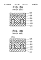
- FIGS. 6A to 6E are sectional views showing a method of manufacturing a semiconductor device in sequential order according to a third embodiment of the present invention.
- a first silicon oxide film 21 with a thickness of, for example, 0.1 ⁇ m is formed on a semiconductor substrate (not shown).
- An HSQ film 22 having a thickness of, for example, 0.4 ⁇ m and a dielectric constant lower than that of a silicon oxide film is formed on the first silicon oxide film 21 by application and annealing.
- a second silicon oxide film 23 with a thickness of, for example, 0.05 ⁇ m is deposited on the HSQ film 22.
- an HSQ film with a dielectric constant lower than that of a silicon oxide film is applied and annealed and these steps are repeated several times, whereby an interlayer HSQ film 69 with a thickness of, for example, 1.2 ⁇ m is formed on the entire surface.
- a third silicon oxide film 70 with a thickness of, for example, 0.05 ⁇ m is then deposited on the interlayer HSQ film 69.
- a TiN film 71 with a thickness of, for example, 0.05 ⁇ m is further deposited on the third silicon oxide film 70.
- a fourth silicon oxide film 76 with a thickness of, for example, 0.05 ⁇ m is deposited on the TiN film 71.
Landscapes
- Engineering & Computer Science (AREA)
- Physics & Mathematics (AREA)
- Microelectronics & Electronic Packaging (AREA)
- General Physics & Mathematics (AREA)
- Manufacturing & Machinery (AREA)
- Computer Hardware Design (AREA)
- Condensed Matter Physics & Semiconductors (AREA)
- Power Engineering (AREA)
- Chemical & Material Sciences (AREA)
- Chemical Kinetics & Catalysis (AREA)
- General Chemical & Material Sciences (AREA)
- Plasma & Fusion (AREA)
- Inorganic Chemistry (AREA)
- Internal Circuitry In Semiconductor Integrated Circuit Devices (AREA)
- Drying Of Semiconductors (AREA)
Abstract
Description
Claims (9)
Priority Applications (1)
| Application Number | Priority Date | Filing Date | Title |
|---|---|---|---|
| US09/439,809 US6225217B1 (en) | 1997-06-27 | 1999-11-12 | Method of manufacturing semiconductor device having multilayer wiring |
Applications Claiming Priority (2)
| Application Number | Priority Date | Filing Date | Title |
|---|---|---|---|
| JP17205697A JP3390329B2 (en) | 1997-06-27 | 1997-06-27 | Semiconductor device and manufacturing method thereof |
| JP9-172056 | 1997-06-27 |
Related Child Applications (1)
| Application Number | Title | Priority Date | Filing Date |
|---|---|---|---|
| US09/439,809 Division US6225217B1 (en) | 1997-06-27 | 1999-11-12 | Method of manufacturing semiconductor device having multilayer wiring |
Publications (1)
| Publication Number | Publication Date |
|---|---|
| US6140225A true US6140225A (en) | 2000-10-31 |
Family
ID=15934725
Family Applications (2)
| Application Number | Title | Priority Date | Filing Date |
|---|---|---|---|
| US09/104,714 Expired - Lifetime US6140225A (en) | 1997-06-27 | 1998-06-25 | Method of manufacturing semiconductor device having multilayer wiring |
| US09/439,809 Expired - Lifetime US6225217B1 (en) | 1997-06-27 | 1999-11-12 | Method of manufacturing semiconductor device having multilayer wiring |
Family Applications After (1)
| Application Number | Title | Priority Date | Filing Date |
|---|---|---|---|
| US09/439,809 Expired - Lifetime US6225217B1 (en) | 1997-06-27 | 1999-11-12 | Method of manufacturing semiconductor device having multilayer wiring |
Country Status (6)
| Country | Link |
|---|---|
| US (2) | US6140225A (en) |
| JP (1) | JP3390329B2 (en) |
| KR (1) | KR100321571B1 (en) |
| CN (1) | CN1139971C (en) |
| GB (1) | GB2326765B (en) |
| TW (1) | TW405163B (en) |
Cited By (11)
| Publication number | Priority date | Publication date | Assignee | Title |
|---|---|---|---|---|
| US20030067078A1 (en) * | 1999-07-13 | 2003-04-10 | Nec Corporation | Semiconductor device and method of manufacturing the same |
| US6638851B2 (en) * | 2001-05-01 | 2003-10-28 | Infineon Technologies North America Corp. | Dual hardmask single damascene integration scheme in an organic low k ILD |
| US20040248395A1 (en) * | 2003-06-05 | 2004-12-09 | Semiconductor Leading Edge Technologies, Inc. | Method for manufacturing semiconductor device |
| US6833331B2 (en) * | 1999-03-31 | 2004-12-21 | Hitachi Ltd. | Method of manufacturing semiconductor integrated circuit device having insulating film formed from liquid substance containing polymer of silicon, oxygen, and hydrogen |
| US6930037B2 (en) * | 1999-12-28 | 2005-08-16 | Nec Electronics Corporation | Process for forming a metal interconnect |
| US20050186775A1 (en) * | 2004-02-23 | 2005-08-25 | Nanya Technology Corporation | Conducting wire and contact opening forming method for reducing photoresist thickness and via resistance |
| US7132362B2 (en) * | 2001-02-21 | 2006-11-07 | Samsung Electronics Co., Ltd. | Semiconductor device with contacts having uniform contact resistance and method for manufacturing the same |
| US20090092930A1 (en) * | 2007-10-04 | 2009-04-09 | Masayuki Endo | Pattern formation method |
| US20120302068A1 (en) * | 2011-05-24 | 2012-11-29 | Chun-Lung Chen | Method for manufacturing semiconductor integrated circuit |
| US20150206794A1 (en) * | 2014-01-17 | 2015-07-23 | Taiwan Semiconductor Manufacturing Company, Ltd. | Method for Removing Micro Scratches In Chemical Mechanical Polishing Processes |
| US9876022B1 (en) | 2016-09-23 | 2018-01-23 | Toshiba Memory Corporation | Method for manufacturing semiconductor device |
Families Citing this family (42)
| Publication number | Priority date | Publication date | Assignee | Title |
|---|---|---|---|---|
| US5989623A (en) * | 1997-08-19 | 1999-11-23 | Applied Materials, Inc. | Dual damascene metallization |
| US7804115B2 (en) * | 1998-02-25 | 2010-09-28 | Micron Technology, Inc. | Semiconductor constructions having antireflective portions |
| US6274292B1 (en) * | 1998-02-25 | 2001-08-14 | Micron Technology, Inc. | Semiconductor processing methods |
| JP3469771B2 (en) * | 1998-03-24 | 2003-11-25 | 富士通株式会社 | Semiconductor device and manufacturing method thereof |
| FR2777697B1 (en) * | 1998-04-16 | 2000-06-09 | St Microelectronics Sa | INTEGRATED CIRCUIT WITH STOP LAYER AND MANUFACTURING METHOD THEREOF |
| US20010029091A1 (en) * | 1998-04-17 | 2001-10-11 | U.S. Philips Corporation | Method for manufacturing an electronic device comprising an organic- containing material |
| US6268282B1 (en) | 1998-09-03 | 2001-07-31 | Micron Technology, Inc. | Semiconductor processing methods of forming and utilizing antireflective material layers, and methods of forming transistor gate stacks |
| US6281100B1 (en) | 1998-09-03 | 2001-08-28 | Micron Technology, Inc. | Semiconductor processing methods |
| US6309801B1 (en) * | 1998-11-18 | 2001-10-30 | U.S. Philips Corporation | Method of manufacturing an electronic device comprising two layers of organic-containing material |
| GB2389963A (en) * | 1998-12-04 | 2003-12-24 | Nec Electronics Corp | Semiconductor device and method of manufacture |
| US6828683B2 (en) | 1998-12-23 | 2004-12-07 | Micron Technology, Inc. | Semiconductor devices, and semiconductor processing methods |
| US7235499B1 (en) * | 1999-01-20 | 2007-06-26 | Micron Technology, Inc. | Semiconductor processing methods |
| JP3436221B2 (en) | 1999-03-15 | 2003-08-11 | ソニー株式会社 | Manufacturing method of semiconductor device |
| JP2000294631A (en) * | 1999-04-05 | 2000-10-20 | Mitsubishi Electric Corp | Semiconductor device and manufacture of the same |
| WO2001003173A1 (en) * | 1999-07-01 | 2001-01-11 | Lam Research Corporation | Method for patterning a layer of a low dielectric constant material |
| JP4471243B2 (en) * | 1999-08-27 | 2010-06-02 | 東京エレクトロン株式会社 | Etching method and plasma processing method |
| JP3348706B2 (en) | 1999-09-29 | 2002-11-20 | 日本電気株式会社 | Method for manufacturing semiconductor device |
| US6541367B1 (en) | 2000-01-18 | 2003-04-01 | Applied Materials, Inc. | Very low dielectric constant plasma-enhanced CVD films |
| US6440860B1 (en) * | 2000-01-18 | 2002-08-27 | Micron Technology, Inc. | Semiconductor processing methods of transferring patterns from patterned photoresists to materials, and structures comprising silicon nitride |
| US6444557B1 (en) | 2000-03-14 | 2002-09-03 | International Business Machines Corporation | Method of forming a damascene structure using a sacrificial conductive layer |
| JP2001338978A (en) | 2000-05-25 | 2001-12-07 | Hitachi Ltd | Semiconductor device and its manufacturing method |
| JP3415602B2 (en) | 2000-06-26 | 2003-06-09 | 鹿児島日本電気株式会社 | Pattern formation method |
| US6500752B2 (en) * | 2000-07-21 | 2002-12-31 | Canon Sales Co., Inc. | Semiconductor device and semiconductor device manufacturing method |
| US6500754B1 (en) * | 2000-11-02 | 2002-12-31 | Advanced Micro Devices, Inc. | Anneal hillock suppression method in integrated circuit interconnects |
| US6348410B1 (en) * | 2000-11-02 | 2002-02-19 | Advanced Micro Devices, Inc. | Low temperature hillock suppression method in integrated circuit interconnects |
| JP2002208633A (en) * | 2001-01-10 | 2002-07-26 | Matsushita Electric Ind Co Ltd | Semiconductor device and its manufacturing method |
| KR100422348B1 (en) * | 2001-06-15 | 2004-03-12 | 주식회사 하이닉스반도체 | Method for fabricating semiconductor device |
| US20030064582A1 (en) * | 2001-09-28 | 2003-04-03 | Oladeji Isaiah O. | Mask layer and interconnect structure for dual damascene semiconductor manufacturing |
| TW506105B (en) * | 2001-10-26 | 2002-10-11 | Nanya Technology Corp | Method for forming interconnect |
| DE10240099A1 (en) * | 2002-08-30 | 2004-03-11 | Infineon Technologies Ag | Production of a semiconductor structure comprises preparing a semiconductor substrate, providing a lower first, a middle second and an upper third mask layer on a surface of the substrate, and further processing |
| GB2394879B (en) * | 2002-11-04 | 2005-11-23 | Electrolux Outdoor Prod Ltd | Trimmer |
| JP4068072B2 (en) * | 2003-01-29 | 2008-03-26 | Necエレクトロニクス株式会社 | Semiconductor device and manufacturing method thereof |
| JP3981026B2 (en) * | 2003-01-30 | 2007-09-26 | 株式会社東芝 | Semiconductor device having multilayer wiring layer and method for manufacturing the same |
| JP2007005840A (en) * | 2006-10-16 | 2007-01-11 | Renesas Technology Corp | Method of manufacturing semiconductor integrated circuit device |
| JP4745370B2 (en) * | 2008-06-11 | 2011-08-10 | ルネサスエレクトロニクス株式会社 | Manufacturing method of semiconductor device |
| CN102222640B (en) * | 2010-04-16 | 2013-08-14 | 中芯国际集成电路制造(上海)有限公司 | Through hole forming method |
| JP4819188B2 (en) * | 2011-02-02 | 2011-11-24 | ルネサスエレクトロニクス株式会社 | Manufacturing method of semiconductor device |
| JP5857690B2 (en) * | 2011-12-02 | 2016-02-10 | 富士通セミコンダクター株式会社 | Manufacturing method of semiconductor device |
| JP5942867B2 (en) * | 2013-01-22 | 2016-06-29 | 富士通株式会社 | Manufacturing method of semiconductor device |
| CN104078362A (en) * | 2013-03-29 | 2014-10-01 | 中国科学院微电子研究所 | Semiconductor device manufacturing method |
| JP6197381B2 (en) * | 2013-06-05 | 2017-09-20 | 富士通セミコンダクター株式会社 | Semiconductor device and manufacturing method thereof |
| CN112041671B (en) * | 2020-07-24 | 2023-10-20 | 长江存储科技有限责任公司 | Method for preparing and analyzing thin film |
Citations (14)
| Publication number | Priority date | Publication date | Assignee | Title |
|---|---|---|---|---|
| US3846166A (en) * | 1971-09-25 | 1974-11-05 | Hitachi Ltd | Method of producing multilayer wiring structure of integrated circuit |
| US4357203A (en) * | 1981-12-30 | 1982-11-02 | Rca Corporation | Plasma etching of polyimide |
| EP0103879A1 (en) * | 1982-09-21 | 1984-03-28 | Siemens Aktiengesellschaft | Method of manufacturing a monolithic integrated circuit |
| GB2137808A (en) * | 1983-04-06 | 1984-10-10 | Plessey Co Plc | Integrated circuit processing method |
| JPH03203240A (en) * | 1989-12-28 | 1991-09-04 | Fujitsu Ltd | Method of manufacturing semiconductor device |
| JPH04167596A (en) * | 1990-10-31 | 1992-06-15 | Nec Corp | Multilayer wiring board |
| JPH0722411A (en) * | 1993-06-22 | 1995-01-24 | Kawasaki Steel Corp | Formation of embedded plug |
| US5442237A (en) * | 1991-10-21 | 1995-08-15 | Motorola Inc. | Semiconductor device having a low permittivity dielectric |
| EP0680084A1 (en) * | 1994-04-28 | 1995-11-02 | Texas Instruments Incorporated | Self-aligned via using low permittivity dielectric |
| JPH0864679A (en) * | 1994-05-27 | 1996-03-08 | Texas Instr Inc <Ti> | Porous dielectric for reducing line capacity |
| JPH0950993A (en) * | 1995-08-08 | 1997-02-18 | Fujitsu Ltd | Formation of insulating film and semiconductor device |
| EP0822586A2 (en) * | 1996-07-30 | 1998-02-04 | Texas Instruments Inc. | Improvements in or relating to integrated circuits |
| EP0834916A2 (en) * | 1996-10-07 | 1998-04-08 | Motorola, Inc. | Method for manufacturing a semiconductor structure comprising regions formed with low dielectric constant material |
| US5935868A (en) * | 1997-03-31 | 1999-08-10 | Intel Corporation | Interconnect structure and method to achieve unlanded vias for low dielectric constant materials |
Family Cites Families (2)
| Publication number | Priority date | Publication date | Assignee | Title |
|---|---|---|---|---|
| US5504042A (en) * | 1994-06-23 | 1996-04-02 | Texas Instruments Incorporated | Porous dielectric material with improved pore surface properties for electronics applications |
| US5573633A (en) * | 1995-11-14 | 1996-11-12 | International Business Machines Corporation | Method of chemically mechanically polishing an electronic component |
-
1997
- 1997-06-27 JP JP17205697A patent/JP3390329B2/en not_active Expired - Fee Related
-
1998
- 1998-06-25 GB GB9813799A patent/GB2326765B/en not_active Expired - Fee Related
- 1998-06-25 US US09/104,714 patent/US6140225A/en not_active Expired - Lifetime
- 1998-06-26 TW TW087110360A patent/TW405163B/en not_active IP Right Cessation
- 1998-06-26 CN CNB981026613A patent/CN1139971C/en not_active Expired - Fee Related
- 1998-06-27 KR KR1019980024553A patent/KR100321571B1/en not_active IP Right Cessation
-
1999
- 1999-11-12 US US09/439,809 patent/US6225217B1/en not_active Expired - Lifetime
Patent Citations (14)
| Publication number | Priority date | Publication date | Assignee | Title |
|---|---|---|---|---|
| US3846166A (en) * | 1971-09-25 | 1974-11-05 | Hitachi Ltd | Method of producing multilayer wiring structure of integrated circuit |
| US4357203A (en) * | 1981-12-30 | 1982-11-02 | Rca Corporation | Plasma etching of polyimide |
| EP0103879A1 (en) * | 1982-09-21 | 1984-03-28 | Siemens Aktiengesellschaft | Method of manufacturing a monolithic integrated circuit |
| GB2137808A (en) * | 1983-04-06 | 1984-10-10 | Plessey Co Plc | Integrated circuit processing method |
| JPH03203240A (en) * | 1989-12-28 | 1991-09-04 | Fujitsu Ltd | Method of manufacturing semiconductor device |
| JPH04167596A (en) * | 1990-10-31 | 1992-06-15 | Nec Corp | Multilayer wiring board |
| US5442237A (en) * | 1991-10-21 | 1995-08-15 | Motorola Inc. | Semiconductor device having a low permittivity dielectric |
| JPH0722411A (en) * | 1993-06-22 | 1995-01-24 | Kawasaki Steel Corp | Formation of embedded plug |
| EP0680084A1 (en) * | 1994-04-28 | 1995-11-02 | Texas Instruments Incorporated | Self-aligned via using low permittivity dielectric |
| JPH0864679A (en) * | 1994-05-27 | 1996-03-08 | Texas Instr Inc <Ti> | Porous dielectric for reducing line capacity |
| JPH0950993A (en) * | 1995-08-08 | 1997-02-18 | Fujitsu Ltd | Formation of insulating film and semiconductor device |
| EP0822586A2 (en) * | 1996-07-30 | 1998-02-04 | Texas Instruments Inc. | Improvements in or relating to integrated circuits |
| EP0834916A2 (en) * | 1996-10-07 | 1998-04-08 | Motorola, Inc. | Method for manufacturing a semiconductor structure comprising regions formed with low dielectric constant material |
| US5935868A (en) * | 1997-03-31 | 1999-08-10 | Intel Corporation | Interconnect structure and method to achieve unlanded vias for low dielectric constant materials |
Non-Patent Citations (4)
| Title |
|---|
| "Hydrogen Silsesquiroxane (HSQ)" Miyanaga et al; p. 654; 26a-N-6; 43rd Apply. Phys. Letter.; Related Society Lecture Reprints;. |
| "Process Technology for Devices" Monthly Semiconductor World, Feb. (1997); p. 82-84. |
| Hydrogen Silsesquiroxane (HSQ) Miyanaga et al; p. 654; 26a N 6; 43rd Apply. Phys. Letter.; Related Society Lecture Reprints;. * |
| Process Technology for Devices Monthly Semiconductor World, Feb. (1997); p. 82 84. * |
Cited By (15)
| Publication number | Priority date | Publication date | Assignee | Title |
|---|---|---|---|---|
| US6833331B2 (en) * | 1999-03-31 | 2004-12-21 | Hitachi Ltd. | Method of manufacturing semiconductor integrated circuit device having insulating film formed from liquid substance containing polymer of silicon, oxygen, and hydrogen |
| US6559542B1 (en) * | 1999-07-13 | 2003-05-06 | Nec Electronics Corporation | Semiconductor device and method of manufacturing the same |
| US20030067078A1 (en) * | 1999-07-13 | 2003-04-10 | Nec Corporation | Semiconductor device and method of manufacturing the same |
| US6930037B2 (en) * | 1999-12-28 | 2005-08-16 | Nec Electronics Corporation | Process for forming a metal interconnect |
| US7132362B2 (en) * | 2001-02-21 | 2006-11-07 | Samsung Electronics Co., Ltd. | Semiconductor device with contacts having uniform contact resistance and method for manufacturing the same |
| US6638851B2 (en) * | 2001-05-01 | 2003-10-28 | Infineon Technologies North America Corp. | Dual hardmask single damascene integration scheme in an organic low k ILD |
| US20040248395A1 (en) * | 2003-06-05 | 2004-12-09 | Semiconductor Leading Edge Technologies, Inc. | Method for manufacturing semiconductor device |
| US20050186775A1 (en) * | 2004-02-23 | 2005-08-25 | Nanya Technology Corporation | Conducting wire and contact opening forming method for reducing photoresist thickness and via resistance |
| US6979638B2 (en) * | 2004-02-23 | 2005-12-27 | Nanya Technology Corporation | Conducting wire and contact opening forming method for reducing photoresist thickness and via resistance |
| US20090092930A1 (en) * | 2007-10-04 | 2009-04-09 | Masayuki Endo | Pattern formation method |
| US7998663B2 (en) | 2007-10-04 | 2011-08-16 | Panasonic Corporation | Pattern formation method |
| US20120302068A1 (en) * | 2011-05-24 | 2012-11-29 | Chun-Lung Chen | Method for manufacturing semiconductor integrated circuit |
| US8735301B2 (en) * | 2011-05-24 | 2014-05-27 | United Microelectronics Corp. | Method for manufacturing semiconductor integrated circuit |
| US20150206794A1 (en) * | 2014-01-17 | 2015-07-23 | Taiwan Semiconductor Manufacturing Company, Ltd. | Method for Removing Micro Scratches In Chemical Mechanical Polishing Processes |
| US9876022B1 (en) | 2016-09-23 | 2018-01-23 | Toshiba Memory Corporation | Method for manufacturing semiconductor device |
Also Published As
| Publication number | Publication date |
|---|---|
| GB2326765A (en) | 1998-12-30 |
| CN1139971C (en) | 2004-02-25 |
| JP3390329B2 (en) | 2003-03-24 |
| TW405163B (en) | 2000-09-11 |
| KR19990007413A (en) | 1999-01-25 |
| JPH1117008A (en) | 1999-01-22 |
| CN1204142A (en) | 1999-01-06 |
| US6225217B1 (en) | 2001-05-01 |
| GB2326765B (en) | 2000-11-15 |
| KR100321571B1 (en) | 2002-03-08 |
| GB9813799D0 (en) | 1998-08-26 |
Similar Documents
| Publication | Publication Date | Title |
|---|---|---|
| US6140225A (en) | Method of manufacturing semiconductor device having multilayer wiring | |
| US6825562B2 (en) | Damascene structure fabricated using a layer of silicon-based photoresist material | |
| US6780782B1 (en) | Bi-level resist structure and fabrication method for contact holes on semiconductor substrates | |
| US8183694B2 (en) | Reversing tone of patterns on integrated circuit and nanoscale fabrication | |
| US20020155693A1 (en) | Method to form self-aligned anti-via interconnects | |
| JP2009530863A (en) | Organic BARC etching process that can be used to form low-K dual damascene integrated circuits | |
| US6384480B1 (en) | Formation of electrical contacts to conductive elements in the fabrication of semiconductor integrated circuits | |
| US20040219796A1 (en) | Plasma etching process | |
| CN100561729C (en) | Double mosaic structure manufacture method | |
| JP2001230317A (en) | Method for forming multilayer interconnection structure and multilayer interconnection structure for semiconductor device | |
| US6774037B2 (en) | Method integrating polymeric interlayer dielectric in integrated circuits | |
| US6313025B1 (en) | Process for manufacturing an integrated circuit including a dual-damascene structure and an integrated circuit | |
| KR20010098774A (en) | Semiconductor Device and Manufacturing Method of the Device | |
| US20040137709A1 (en) | Metal barrier cap fabrication by polymer lift-off | |
| US6821896B1 (en) | Method to eliminate via poison effect | |
| KR100614782B1 (en) | A process for manufacturing an integrated circuit including a dual- damascene structure and an integrated circuit | |
| JPH09129727A (en) | Semiconductor device and manufacturing method thereof | |
| US20060134921A1 (en) | Plasma etching process | |
| US7192880B2 (en) | Method for line etch roughness (LER) reduction for low-k interconnect damascene trench etching | |
| JPH11162982A (en) | Manufacture of semiconductor device | |
| US6780778B2 (en) | Method for fabricating semiconductor device | |
| JP2005159008A (en) | Manufacturing method of semiconductor device | |
| JP2001345380A (en) | Semiconductor device and method of manufacturing the same | |
| JP3683570B2 (en) | Manufacturing method of semiconductor device | |
| GB2350931A (en) | Forming vias in low-k dielectric materials using metallic masks |
Legal Events
| Date | Code | Title | Description |
|---|---|---|---|
| AS | Assignment |
Owner name: NEC CORPORATION, JAPAN Free format text: ASSIGNMENT OF ASSIGNORS INTEREST;ASSIGNORS:USAMI, TATSUYA;AOKI, HIDEMITSU;TSUCHIYA, YASUAKI;AND OTHERS;REEL/FRAME:009275/0164 Effective date: 19980615 |
|
| STCF | Information on status: patent grant |
Free format text: PATENTED CASE |
|
| FEPP | Fee payment procedure |
Free format text: PAYOR NUMBER ASSIGNED (ORIGINAL EVENT CODE: ASPN); ENTITY STATUS OF PATENT OWNER: LARGE ENTITY |
|
| CC | Certificate of correction | ||
| AS | Assignment |
Owner name: NEC ELECTRONICS CORPORATION, JAPAN Free format text: ASSIGNMENT OF ASSIGNORS INTEREST;ASSIGNOR:NEC CORPORATION;REEL/FRAME:013751/0721 Effective date: 20021101 |
|
| FPAY | Fee payment |
Year of fee payment: 4 |
|
| FPAY | Fee payment |
Year of fee payment: 8 |
|
| AS | Assignment |
Owner name: RENESAS ELECTRONICS CORPORATION, JAPAN Free format text: CHANGE OF NAME;ASSIGNOR:NEC ELECTRONICS CORPORATION;REEL/FRAME:025183/0574 Effective date: 20100401 |
|
| FPAY | Fee payment |
Year of fee payment: 12 |
|
| AS | Assignment |
Owner name: STARBOARD VALUE INTERMEDIATE FUND LP, AS COLLATERAL AGENT, NEW YORK Free format text: PATENT SECURITY AGREEMENT;ASSIGNORS:ACACIA RESEARCH GROUP LLC;AMERICAN VEHICULAR SCIENCES LLC;BONUTTI SKELETAL INNOVATIONS LLC;AND OTHERS;REEL/FRAME:052853/0153 Effective date: 20200604 |
|
| AS | Assignment |
Owner name: CELLULAR COMMUNICATIONS EQUIPMENT LLC, TEXAS Free format text: RELEASE OF SECURITY INTEREST IN PATENTS;ASSIGNOR:STARBOARD VALUE INTERMEDIATE FUND LP;REEL/FRAME:053654/0254 Effective date: 20200630 Owner name: STINGRAY IP SOLUTIONS LLC, TEXAS Free format text: RELEASE OF SECURITY INTEREST IN PATENTS;ASSIGNOR:STARBOARD VALUE INTERMEDIATE FUND LP;REEL/FRAME:053654/0254 Effective date: 20200630 Owner name: LIFEPORT SCIENCES LLC, TEXAS Free format text: RELEASE OF SECURITY INTEREST IN PATENTS;ASSIGNOR:STARBOARD VALUE INTERMEDIATE FUND LP;REEL/FRAME:053654/0254 Effective date: 20200630 Owner name: ACACIA RESEARCH GROUP LLC, NEW YORK Free format text: RELEASE OF SECURITY INTEREST IN PATENTS;ASSIGNOR:STARBOARD VALUE INTERMEDIATE FUND LP;REEL/FRAME:053654/0254 Effective date: 20200630 Owner name: PARTHENON UNIFIED MEMORY ARCHITECTURE LLC, TEXAS Free format text: RELEASE OF SECURITY INTEREST IN PATENTS;ASSIGNOR:STARBOARD VALUE INTERMEDIATE FUND LP;REEL/FRAME:053654/0254 Effective date: 20200630 Owner name: MONARCH NETWORKING SOLUTIONS LLC, CALIFORNIA Free format text: RELEASE OF SECURITY INTEREST IN PATENTS;ASSIGNOR:STARBOARD VALUE INTERMEDIATE FUND LP;REEL/FRAME:053654/0254 Effective date: 20200630 Owner name: R2 SOLUTIONS LLC, TEXAS Free format text: RELEASE OF SECURITY INTEREST IN PATENTS;ASSIGNOR:STARBOARD VALUE INTERMEDIATE FUND LP;REEL/FRAME:053654/0254 Effective date: 20200630 Owner name: UNIFICATION TECHNOLOGIES LLC, TEXAS Free format text: RELEASE OF SECURITY INTEREST IN PATENTS;ASSIGNOR:STARBOARD VALUE INTERMEDIATE FUND LP;REEL/FRAME:053654/0254 Effective date: 20200630 Owner name: INNOVATIVE DISPLAY TECHNOLOGIES LLC, TEXAS Free format text: RELEASE OF SECURITY INTEREST IN PATENTS;ASSIGNOR:STARBOARD VALUE INTERMEDIATE FUND LP;REEL/FRAME:053654/0254 Effective date: 20200630 Owner name: NEXUS DISPLAY TECHNOLOGIES LLC, TEXAS Free format text: RELEASE OF SECURITY INTEREST IN PATENTS;ASSIGNOR:STARBOARD VALUE INTERMEDIATE FUND LP;REEL/FRAME:053654/0254 Effective date: 20200630 Owner name: MOBILE ENHANCEMENT SOLUTIONS LLC, TEXAS Free format text: RELEASE OF SECURITY INTEREST IN PATENTS;ASSIGNOR:STARBOARD VALUE INTERMEDIATE FUND LP;REEL/FRAME:053654/0254 Effective date: 20200630 Owner name: BONUTTI SKELETAL INNOVATIONS LLC, TEXAS Free format text: RELEASE OF SECURITY INTEREST IN PATENTS;ASSIGNOR:STARBOARD VALUE INTERMEDIATE FUND LP;REEL/FRAME:053654/0254 Effective date: 20200630 Owner name: AMERICAN VEHICULAR SCIENCES LLC, TEXAS Free format text: RELEASE OF SECURITY INTEREST IN PATENTS;ASSIGNOR:STARBOARD VALUE INTERMEDIATE FUND LP;REEL/FRAME:053654/0254 Effective date: 20200630 Owner name: TELECONFERENCE SYSTEMS LLC, TEXAS Free format text: RELEASE OF SECURITY INTEREST IN PATENTS;ASSIGNOR:STARBOARD VALUE INTERMEDIATE FUND LP;REEL/FRAME:053654/0254 Effective date: 20200630 Owner name: LIMESTONE MEMORY SYSTEMS LLC, CALIFORNIA Free format text: RELEASE OF SECURITY INTEREST IN PATENTS;ASSIGNOR:STARBOARD VALUE INTERMEDIATE FUND LP;REEL/FRAME:053654/0254 Effective date: 20200630 Owner name: SAINT LAWRENCE COMMUNICATIONS LLC, TEXAS Free format text: RELEASE OF SECURITY INTEREST IN PATENTS;ASSIGNOR:STARBOARD VALUE INTERMEDIATE FUND LP;REEL/FRAME:053654/0254 Effective date: 20200630 Owner name: SUPER INTERCONNECT TECHNOLOGIES LLC, TEXAS Free format text: RELEASE OF SECURITY INTEREST IN PATENTS;ASSIGNOR:STARBOARD VALUE INTERMEDIATE FUND LP;REEL/FRAME:053654/0254 Effective date: 20200630 |
|
| AS | Assignment |
Owner name: STARBOARD VALUE INTERMEDIATE FUND LP, AS COLLATERAL AGENT, NEW YORK Free format text: CORRECTIVE ASSIGNMENT TO CORRECT THE ASSIGNOR NAME PREVIOUSLY RECORDED ON REEL 052853 FRAME 0153. ASSIGNOR(S) HEREBY CONFIRMS THE PATENT SECURITY AGREEMENT;ASSIGNOR:ACACIA RESEARCH GROUP LLC;REEL/FRAME:056775/0066 Effective date: 20200604 |
|
| AS | Assignment |
Owner name: ACACIA RESEARCH GROUP LLC, NEW YORK Free format text: CORRECTIVE ASSIGNMENT TO CORRECT THE ASSIGNEE NAME PREVIOUSLY RECORDED AT REEL: 053654 FRAME: 0254. ASSIGNOR(S) HEREBY CONFIRMS THE ASSIGNMENT;ASSIGNOR:STARBOARD VALUE INTERMEDIATE FUND LP;REEL/FRAME:057454/0045 Effective date: 20200630 |