US6140225A - Method of manufacturing semiconductor device having multilayer wiring - Google Patents
Method of manufacturing semiconductor device having multilayer wiring Download PDFInfo
- Publication number
- US6140225A US6140225A US09/104,714 US10471498A US6140225A US 6140225 A US6140225 A US 6140225A US 10471498 A US10471498 A US 10471498A US 6140225 A US6140225 A US 6140225A
- Authority
- US
- United States
- Prior art keywords
- film
- silicon oxide
- insulating film
- semiconductor device
- oxide film
- Prior art date
- Legal status (The legal status is an assumption and is not a legal conclusion. Google has not performed a legal analysis and makes no representation as to the accuracy of the status listed.)
- Expired - Lifetime
Links
Images


Classifications
-
- H10P14/662—
-
- H10D64/011—
-
- H10P14/40—
-
- H10P14/665—
-
- H10P14/687—
-
- H10P14/69215—
-
- H10P14/6925—
-
- H10P50/267—
-
- H10P50/287—
-
- H10P50/71—
-
- H10P50/73—
-
- H10P76/405—
-
- H10W20/081—
-
- H10W20/087—
-
- H10W20/088—
Definitions
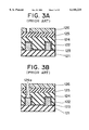
- FIGS. 6A to 6E are sectional views showing a method of manufacturing a semiconductor device in sequential order according to a third embodiment of the present invention.
- a first silicon oxide film 21 with a thickness of, for example, 0.1 ⁇ m is formed on a semiconductor substrate (not shown).
- An HSQ film 22 having a thickness of, for example, 0.4 ⁇ m and a dielectric constant lower than that of a silicon oxide film is formed on the first silicon oxide film 21 by application and annealing.
- a second silicon oxide film 23 with a thickness of, for example, 0.05 ⁇ m is deposited on the HSQ film 22.
- an HSQ film with a dielectric constant lower than that of a silicon oxide film is applied and annealed and these steps are repeated several times, whereby an interlayer HSQ film 69 with a thickness of, for example, 1.2 ⁇ m is formed on the entire surface.
- a third silicon oxide film 70 with a thickness of, for example, 0.05 ⁇ m is then deposited on the interlayer HSQ film 69.
- a TiN film 71 with a thickness of, for example, 0.05 ⁇ m is further deposited on the third silicon oxide film 70.
- a fourth silicon oxide film 76 with a thickness of, for example, 0.05 ⁇ m is deposited on the TiN film 71.
Landscapes
- Internal Circuitry In Semiconductor Integrated Circuit Devices (AREA)
- Drying Of Semiconductors (AREA)
Abstract
Description
Claims (9)
Priority Applications (1)
| Application Number | Priority Date | Filing Date | Title |
|---|---|---|---|
| US09/439,809 US6225217B1 (en) | 1997-06-27 | 1999-11-12 | Method of manufacturing semiconductor device having multilayer wiring |
Applications Claiming Priority (2)
| Application Number | Priority Date | Filing Date | Title |
|---|---|---|---|
| JP9-172056 | 1997-06-27 | ||
| JP17205697A JP3390329B2 (en) | 1997-06-27 | 1997-06-27 | Semiconductor device and manufacturing method thereof |
Related Child Applications (1)
| Application Number | Title | Priority Date | Filing Date |
|---|---|---|---|
| US09/439,809 Division US6225217B1 (en) | 1997-06-27 | 1999-11-12 | Method of manufacturing semiconductor device having multilayer wiring |
Publications (1)
| Publication Number | Publication Date |
|---|---|
| US6140225A true US6140225A (en) | 2000-10-31 |
Family
ID=15934725
Family Applications (2)
| Application Number | Title | Priority Date | Filing Date |
|---|---|---|---|
| US09/104,714 Expired - Lifetime US6140225A (en) | 1997-06-27 | 1998-06-25 | Method of manufacturing semiconductor device having multilayer wiring |
| US09/439,809 Expired - Lifetime US6225217B1 (en) | 1997-06-27 | 1999-11-12 | Method of manufacturing semiconductor device having multilayer wiring |
Family Applications After (1)
| Application Number | Title | Priority Date | Filing Date |
|---|---|---|---|
| US09/439,809 Expired - Lifetime US6225217B1 (en) | 1997-06-27 | 1999-11-12 | Method of manufacturing semiconductor device having multilayer wiring |
Country Status (6)
| Country | Link |
|---|---|
| US (2) | US6140225A (en) |
| JP (1) | JP3390329B2 (en) |
| KR (1) | KR100321571B1 (en) |
| CN (1) | CN1139971C (en) |
| GB (1) | GB2326765B (en) |
| TW (1) | TW405163B (en) |
Cited By (11)
| Publication number | Priority date | Publication date | Assignee | Title |
|---|---|---|---|---|
| US20030067078A1 (en) * | 1999-07-13 | 2003-04-10 | Nec Corporation | Semiconductor device and method of manufacturing the same |
| US6638851B2 (en) * | 2001-05-01 | 2003-10-28 | Infineon Technologies North America Corp. | Dual hardmask single damascene integration scheme in an organic low k ILD |
| US20040248395A1 (en) * | 2003-06-05 | 2004-12-09 | Semiconductor Leading Edge Technologies, Inc. | Method for manufacturing semiconductor device |
| US6833331B2 (en) * | 1999-03-31 | 2004-12-21 | Hitachi Ltd. | Method of manufacturing semiconductor integrated circuit device having insulating film formed from liquid substance containing polymer of silicon, oxygen, and hydrogen |
| US6930037B2 (en) * | 1999-12-28 | 2005-08-16 | Nec Electronics Corporation | Process for forming a metal interconnect |
| US20050186775A1 (en) * | 2004-02-23 | 2005-08-25 | Nanya Technology Corporation | Conducting wire and contact opening forming method for reducing photoresist thickness and via resistance |
| US7132362B2 (en) * | 2001-02-21 | 2006-11-07 | Samsung Electronics Co., Ltd. | Semiconductor device with contacts having uniform contact resistance and method for manufacturing the same |
| US20090092930A1 (en) * | 2007-10-04 | 2009-04-09 | Masayuki Endo | Pattern formation method |
| US20120302068A1 (en) * | 2011-05-24 | 2012-11-29 | Chun-Lung Chen | Method for manufacturing semiconductor integrated circuit |
| US20150206794A1 (en) * | 2014-01-17 | 2015-07-23 | Taiwan Semiconductor Manufacturing Company, Ltd. | Method for Removing Micro Scratches In Chemical Mechanical Polishing Processes |
| US9876022B1 (en) | 2016-09-23 | 2018-01-23 | Toshiba Memory Corporation | Method for manufacturing semiconductor device |
Families Citing this family (43)
| Publication number | Priority date | Publication date | Assignee | Title |
|---|---|---|---|---|
| US5989623A (en) * | 1997-08-19 | 1999-11-23 | Applied Materials, Inc. | Dual damascene metallization |
| US6274292B1 (en) * | 1998-02-25 | 2001-08-14 | Micron Technology, Inc. | Semiconductor processing methods |
| US7804115B2 (en) * | 1998-02-25 | 2010-09-28 | Micron Technology, Inc. | Semiconductor constructions having antireflective portions |
| JP3469771B2 (en) * | 1998-03-24 | 2003-11-25 | 富士通株式会社 | Semiconductor device and manufacturing method thereof |
| FR2777697B1 (en) * | 1998-04-16 | 2000-06-09 | St Microelectronics Sa | INTEGRATED CIRCUIT WITH STOP LAYER AND MANUFACTURING METHOD THEREOF |
| US20010029091A1 (en) * | 1998-04-17 | 2001-10-11 | U.S. Philips Corporation | Method for manufacturing an electronic device comprising an organic- containing material |
| US6281100B1 (en) | 1998-09-03 | 2001-08-28 | Micron Technology, Inc. | Semiconductor processing methods |
| US6268282B1 (en) | 1998-09-03 | 2001-07-31 | Micron Technology, Inc. | Semiconductor processing methods of forming and utilizing antireflective material layers, and methods of forming transistor gate stacks |
| US6309801B1 (en) | 1998-11-18 | 2001-10-30 | U.S. Philips Corporation | Method of manufacturing an electronic device comprising two layers of organic-containing material |
| GB2389963A (en) * | 1998-12-04 | 2003-12-24 | Nec Electronics Corp | Semiconductor device and method of manufacture |
| US6828683B2 (en) | 1998-12-23 | 2004-12-07 | Micron Technology, Inc. | Semiconductor devices, and semiconductor processing methods |
| US7235499B1 (en) * | 1999-01-20 | 2007-06-26 | Micron Technology, Inc. | Semiconductor processing methods |
| JP3436221B2 (en) | 1999-03-15 | 2003-08-11 | ソニー株式会社 | Manufacturing method of semiconductor device |
| JP2000294631A (en) * | 1999-04-05 | 2000-10-20 | Mitsubishi Electric Corp | Semiconductor device and manufacturing method thereof |
| WO2001003173A1 (en) * | 1999-07-01 | 2001-01-11 | Lam Research Corporation | Method for patterning a layer of a low dielectric constant material |
| JP4471243B2 (en) | 1999-08-27 | 2010-06-02 | 東京エレクトロン株式会社 | Etching method and plasma processing method |
| US7067414B1 (en) | 1999-09-01 | 2006-06-27 | Micron Technology, Inc. | Low k interlevel dielectric layer fabrication methods |
| JP3348706B2 (en) | 1999-09-29 | 2002-11-20 | 日本電気株式会社 | Method for manufacturing semiconductor device |
| US6541367B1 (en) | 2000-01-18 | 2003-04-01 | Applied Materials, Inc. | Very low dielectric constant plasma-enhanced CVD films |
| US6440860B1 (en) * | 2000-01-18 | 2002-08-27 | Micron Technology, Inc. | Semiconductor processing methods of transferring patterns from patterned photoresists to materials, and structures comprising silicon nitride |
| US6444557B1 (en) * | 2000-03-14 | 2002-09-03 | International Business Machines Corporation | Method of forming a damascene structure using a sacrificial conductive layer |
| JP2001338978A (en) | 2000-05-25 | 2001-12-07 | Hitachi Ltd | Semiconductor device and manufacturing method thereof |
| JP3415602B2 (en) | 2000-06-26 | 2003-06-09 | 鹿児島日本電気株式会社 | Pattern formation method |
| US6500752B2 (en) * | 2000-07-21 | 2002-12-31 | Canon Sales Co., Inc. | Semiconductor device and semiconductor device manufacturing method |
| US6500754B1 (en) * | 2000-11-02 | 2002-12-31 | Advanced Micro Devices, Inc. | Anneal hillock suppression method in integrated circuit interconnects |
| US6348410B1 (en) * | 2000-11-02 | 2002-02-19 | Advanced Micro Devices, Inc. | Low temperature hillock suppression method in integrated circuit interconnects |
| JP2002208633A (en) * | 2001-01-10 | 2002-07-26 | Matsushita Electric Ind Co Ltd | Semiconductor device and method of manufacturing the same |
| KR100422348B1 (en) * | 2001-06-15 | 2004-03-12 | 주식회사 하이닉스반도체 | Method for fabricating semiconductor device |
| US20030064582A1 (en) * | 2001-09-28 | 2003-04-03 | Oladeji Isaiah O. | Mask layer and interconnect structure for dual damascene semiconductor manufacturing |
| TW506105B (en) * | 2001-10-26 | 2002-10-11 | Nanya Technology Corp | Method for forming interconnect |
| DE10240099A1 (en) * | 2002-08-30 | 2004-03-11 | Infineon Technologies Ag | Production of a semiconductor structure comprises preparing a semiconductor substrate, providing a lower first, a middle second and an upper third mask layer on a surface of the substrate, and further processing |
| GB2394879B (en) * | 2002-11-04 | 2005-11-23 | Electrolux Outdoor Prod Ltd | Trimmer |
| JP4068072B2 (en) * | 2003-01-29 | 2008-03-26 | Necエレクトロニクス株式会社 | Semiconductor device and manufacturing method thereof |
| JP3981026B2 (en) * | 2003-01-30 | 2007-09-26 | 株式会社東芝 | Semiconductor device having multilayer wiring layer and method for manufacturing the same |
| JP2007005840A (en) * | 2006-10-16 | 2007-01-11 | Renesas Technology Corp | Method of manufacturing semiconductor integrated circuit device |
| JP4745370B2 (en) * | 2008-06-11 | 2011-08-10 | ルネサスエレクトロニクス株式会社 | Manufacturing method of semiconductor device |
| CN102222640B (en) * | 2010-04-16 | 2013-08-14 | 中芯国际集成电路制造(上海)有限公司 | Through hole forming method |
| JP4819188B2 (en) * | 2011-02-02 | 2011-11-24 | ルネサスエレクトロニクス株式会社 | Manufacturing method of semiconductor device |
| JP5857690B2 (en) * | 2011-12-02 | 2016-02-10 | 富士通セミコンダクター株式会社 | Manufacturing method of semiconductor device |
| JP5942867B2 (en) * | 2013-01-22 | 2016-06-29 | 富士通株式会社 | Manufacturing method of semiconductor device |
| CN104078362A (en) * | 2013-03-29 | 2014-10-01 | 中国科学院微电子研究所 | Semiconductor device manufacturing method |
| JP6197381B2 (en) * | 2013-06-05 | 2017-09-20 | 富士通セミコンダクター株式会社 | Semiconductor device and manufacturing method thereof |
| CN112041671B (en) * | 2020-07-24 | 2023-10-20 | 长江存储科技有限责任公司 | Methods of Preparing and Analyzing Thin Films |
Citations (14)
| Publication number | Priority date | Publication date | Assignee | Title |
|---|---|---|---|---|
| US3846166A (en) * | 1971-09-25 | 1974-11-05 | Hitachi Ltd | Method of producing multilayer wiring structure of integrated circuit |
| US4357203A (en) * | 1981-12-30 | 1982-11-02 | Rca Corporation | Plasma etching of polyimide |
| EP0103879A1 (en) * | 1982-09-21 | 1984-03-28 | Siemens Aktiengesellschaft | Method of manufacturing a monolithic integrated circuit |
| GB2137808A (en) * | 1983-04-06 | 1984-10-10 | Plessey Co Plc | Integrated circuit processing method |
| JPH03203240A (en) * | 1989-12-28 | 1991-09-04 | Fujitsu Ltd | Method of manufacturing semiconductor device |
| JPH04167596A (en) * | 1990-10-31 | 1992-06-15 | Nec Corp | Multilayer wiring board |
| JPH0722411A (en) * | 1993-06-22 | 1995-01-24 | Kawasaki Steel Corp | Method of forming embedded plug |
| US5442237A (en) * | 1991-10-21 | 1995-08-15 | Motorola Inc. | Semiconductor device having a low permittivity dielectric |
| EP0680084A1 (en) * | 1994-04-28 | 1995-11-02 | Texas Instruments Incorporated | Self-aligned via using low permittivity dielectric |
| JPH0864679A (en) * | 1994-05-27 | 1996-03-08 | Texas Instr Inc <Ti> | Porous dielectric for reducing line capacitance |
| JPH0950993A (en) * | 1995-08-08 | 1997-02-18 | Fujitsu Ltd | Insulating film forming method and semiconductor device |
| EP0822586A2 (en) * | 1996-07-30 | 1998-02-04 | Texas Instruments Inc. | Improvements in or relating to integrated circuits |
| EP0834916A2 (en) * | 1996-10-07 | 1998-04-08 | Motorola, Inc. | Method for manufacturing a semiconductor structure comprising regions formed with low dielectric constant material |
| US5935868A (en) * | 1997-03-31 | 1999-08-10 | Intel Corporation | Interconnect structure and method to achieve unlanded vias for low dielectric constant materials |
Family Cites Families (2)
| Publication number | Priority date | Publication date | Assignee | Title |
|---|---|---|---|---|
| US5504042A (en) * | 1994-06-23 | 1996-04-02 | Texas Instruments Incorporated | Porous dielectric material with improved pore surface properties for electronics applications |
| US5573633A (en) * | 1995-11-14 | 1996-11-12 | International Business Machines Corporation | Method of chemically mechanically polishing an electronic component |
-
1997
- 1997-06-27 JP JP17205697A patent/JP3390329B2/en not_active Expired - Fee Related
-
1998
- 1998-06-25 US US09/104,714 patent/US6140225A/en not_active Expired - Lifetime
- 1998-06-25 GB GB9813799A patent/GB2326765B/en not_active Expired - Fee Related
- 1998-06-26 TW TW087110360A patent/TW405163B/en not_active IP Right Cessation
- 1998-06-26 CN CNB981026613A patent/CN1139971C/en not_active Expired - Fee Related
- 1998-06-27 KR KR1019980024553A patent/KR100321571B1/en not_active Expired - Fee Related
-
1999
- 1999-11-12 US US09/439,809 patent/US6225217B1/en not_active Expired - Lifetime
Patent Citations (14)
| Publication number | Priority date | Publication date | Assignee | Title |
|---|---|---|---|---|
| US3846166A (en) * | 1971-09-25 | 1974-11-05 | Hitachi Ltd | Method of producing multilayer wiring structure of integrated circuit |
| US4357203A (en) * | 1981-12-30 | 1982-11-02 | Rca Corporation | Plasma etching of polyimide |
| EP0103879A1 (en) * | 1982-09-21 | 1984-03-28 | Siemens Aktiengesellschaft | Method of manufacturing a monolithic integrated circuit |
| GB2137808A (en) * | 1983-04-06 | 1984-10-10 | Plessey Co Plc | Integrated circuit processing method |
| JPH03203240A (en) * | 1989-12-28 | 1991-09-04 | Fujitsu Ltd | Method of manufacturing semiconductor device |
| JPH04167596A (en) * | 1990-10-31 | 1992-06-15 | Nec Corp | Multilayer wiring board |
| US5442237A (en) * | 1991-10-21 | 1995-08-15 | Motorola Inc. | Semiconductor device having a low permittivity dielectric |
| JPH0722411A (en) * | 1993-06-22 | 1995-01-24 | Kawasaki Steel Corp | Method of forming embedded plug |
| EP0680084A1 (en) * | 1994-04-28 | 1995-11-02 | Texas Instruments Incorporated | Self-aligned via using low permittivity dielectric |
| JPH0864679A (en) * | 1994-05-27 | 1996-03-08 | Texas Instr Inc <Ti> | Porous dielectric for reducing line capacitance |
| JPH0950993A (en) * | 1995-08-08 | 1997-02-18 | Fujitsu Ltd | Insulating film forming method and semiconductor device |
| EP0822586A2 (en) * | 1996-07-30 | 1998-02-04 | Texas Instruments Inc. | Improvements in or relating to integrated circuits |
| EP0834916A2 (en) * | 1996-10-07 | 1998-04-08 | Motorola, Inc. | Method for manufacturing a semiconductor structure comprising regions formed with low dielectric constant material |
| US5935868A (en) * | 1997-03-31 | 1999-08-10 | Intel Corporation | Interconnect structure and method to achieve unlanded vias for low dielectric constant materials |
Non-Patent Citations (4)
| Title |
|---|
| "Hydrogen Silsesquiroxane (HSQ)" Miyanaga et al; p. 654; 26a-N-6; 43rd Apply. Phys. Letter.; Related Society Lecture Reprints;. |
| "Process Technology for Devices" Monthly Semiconductor World, Feb. (1997); p. 82-84. |
| Hydrogen Silsesquiroxane (HSQ) Miyanaga et al; p. 654; 26a N 6; 43rd Apply. Phys. Letter.; Related Society Lecture Reprints;. * |
| Process Technology for Devices Monthly Semiconductor World, Feb. (1997); p. 82 84. * |
Cited By (15)
| Publication number | Priority date | Publication date | Assignee | Title |
|---|---|---|---|---|
| US6833331B2 (en) * | 1999-03-31 | 2004-12-21 | Hitachi Ltd. | Method of manufacturing semiconductor integrated circuit device having insulating film formed from liquid substance containing polymer of silicon, oxygen, and hydrogen |
| US6559542B1 (en) * | 1999-07-13 | 2003-05-06 | Nec Electronics Corporation | Semiconductor device and method of manufacturing the same |
| US20030067078A1 (en) * | 1999-07-13 | 2003-04-10 | Nec Corporation | Semiconductor device and method of manufacturing the same |
| US6930037B2 (en) * | 1999-12-28 | 2005-08-16 | Nec Electronics Corporation | Process for forming a metal interconnect |
| US7132362B2 (en) * | 2001-02-21 | 2006-11-07 | Samsung Electronics Co., Ltd. | Semiconductor device with contacts having uniform contact resistance and method for manufacturing the same |
| US6638851B2 (en) * | 2001-05-01 | 2003-10-28 | Infineon Technologies North America Corp. | Dual hardmask single damascene integration scheme in an organic low k ILD |
| US20040248395A1 (en) * | 2003-06-05 | 2004-12-09 | Semiconductor Leading Edge Technologies, Inc. | Method for manufacturing semiconductor device |
| US20050186775A1 (en) * | 2004-02-23 | 2005-08-25 | Nanya Technology Corporation | Conducting wire and contact opening forming method for reducing photoresist thickness and via resistance |
| US6979638B2 (en) * | 2004-02-23 | 2005-12-27 | Nanya Technology Corporation | Conducting wire and contact opening forming method for reducing photoresist thickness and via resistance |
| US20090092930A1 (en) * | 2007-10-04 | 2009-04-09 | Masayuki Endo | Pattern formation method |
| US7998663B2 (en) | 2007-10-04 | 2011-08-16 | Panasonic Corporation | Pattern formation method |
| US20120302068A1 (en) * | 2011-05-24 | 2012-11-29 | Chun-Lung Chen | Method for manufacturing semiconductor integrated circuit |
| US8735301B2 (en) * | 2011-05-24 | 2014-05-27 | United Microelectronics Corp. | Method for manufacturing semiconductor integrated circuit |
| US20150206794A1 (en) * | 2014-01-17 | 2015-07-23 | Taiwan Semiconductor Manufacturing Company, Ltd. | Method for Removing Micro Scratches In Chemical Mechanical Polishing Processes |
| US9876022B1 (en) | 2016-09-23 | 2018-01-23 | Toshiba Memory Corporation | Method for manufacturing semiconductor device |
Also Published As
| Publication number | Publication date |
|---|---|
| CN1204142A (en) | 1999-01-06 |
| GB9813799D0 (en) | 1998-08-26 |
| CN1139971C (en) | 2004-02-25 |
| GB2326765B (en) | 2000-11-15 |
| KR19990007413A (en) | 1999-01-25 |
| TW405163B (en) | 2000-09-11 |
| GB2326765A (en) | 1998-12-30 |
| KR100321571B1 (en) | 2002-03-08 |
| JPH1117008A (en) | 1999-01-22 |
| US6225217B1 (en) | 2001-05-01 |
| JP3390329B2 (en) | 2003-03-24 |
Similar Documents
| Publication | Publication Date | Title |
|---|---|---|
| US6140225A (en) | Method of manufacturing semiconductor device having multilayer wiring | |
| US6825562B2 (en) | Damascene structure fabricated using a layer of silicon-based photoresist material | |
| US6780782B1 (en) | Bi-level resist structure and fabrication method for contact holes on semiconductor substrates | |
| US8183694B2 (en) | Reversing tone of patterns on integrated circuit and nanoscale fabrication | |
| US20020155693A1 (en) | Method to form self-aligned anti-via interconnects | |
| JP2009530863A (en) | Organic BARC etching process that can be used to form low-K dual damascene integrated circuits | |
| US20040219796A1 (en) | Plasma etching process | |
| US6384480B1 (en) | Formation of electrical contacts to conductive elements in the fabrication of semiconductor integrated circuits | |
| US6774037B2 (en) | Method integrating polymeric interlayer dielectric in integrated circuits | |
| US6313025B1 (en) | Process for manufacturing an integrated circuit including a dual-damascene structure and an integrated circuit | |
| US6821896B1 (en) | Method to eliminate via poison effect | |
| US20040137709A1 (en) | Metal barrier cap fabrication by polymer lift-off | |
| KR20010098774A (en) | Semiconductor Device and Manufacturing Method of the Device | |
| KR100614782B1 (en) | A process for manufacturing an integrated circuit including a dual- damascene structure and an integrated circuit | |
| US7192880B2 (en) | Method for line etch roughness (LER) reduction for low-k interconnect damascene trench etching | |
| CN100561729C (en) | Fabrication method of dual damascene structure | |
| JPH11162982A (en) | Manufacture of semiconductor device | |
| US6780778B2 (en) | Method for fabricating semiconductor device | |
| JP2005159008A (en) | Manufacturing method of semiconductor device | |
| JP2001345380A (en) | Semiconductor device manufacturing method and semiconductor device | |
| US20060134921A1 (en) | Plasma etching process | |
| JP3683570B2 (en) | Manufacturing method of semiconductor device | |
| GB2350931A (en) | Forming vias in low-k dielectric materials using metallic masks | |
| KR0155801B1 (en) | Method of forming multilayer interconnection of semiconductor device | |
| KR101005738B1 (en) | Dual damascene pattern formation method of semiconductor device |
Legal Events
| Date | Code | Title | Description |
|---|---|---|---|
| AS | Assignment |
Owner name: NEC CORPORATION, JAPAN Free format text: ASSIGNMENT OF ASSIGNORS INTEREST;ASSIGNORS:USAMI, TATSUYA;AOKI, HIDEMITSU;TSUCHIYA, YASUAKI;AND OTHERS;REEL/FRAME:009275/0164 Effective date: 19980615 |
|
| STCF | Information on status: patent grant |
Free format text: PATENTED CASE |
|
| FEPP | Fee payment procedure |
Free format text: PAYOR NUMBER ASSIGNED (ORIGINAL EVENT CODE: ASPN); ENTITY STATUS OF PATENT OWNER: LARGE ENTITY |
|
| CC | Certificate of correction | ||
| AS | Assignment |
Owner name: NEC ELECTRONICS CORPORATION, JAPAN Free format text: ASSIGNMENT OF ASSIGNORS INTEREST;ASSIGNOR:NEC CORPORATION;REEL/FRAME:013751/0721 Effective date: 20021101 |
|
| FPAY | Fee payment |
Year of fee payment: 4 |
|
| FPAY | Fee payment |
Year of fee payment: 8 |
|
| AS | Assignment |
Owner name: RENESAS ELECTRONICS CORPORATION, JAPAN Free format text: CHANGE OF NAME;ASSIGNOR:NEC ELECTRONICS CORPORATION;REEL/FRAME:025183/0574 Effective date: 20100401 |
|
| FPAY | Fee payment |
Year of fee payment: 12 |
|
| AS | Assignment |
Owner name: STARBOARD VALUE INTERMEDIATE FUND LP, AS COLLATERAL AGENT, NEW YORK Free format text: PATENT SECURITY AGREEMENT;ASSIGNORS:ACACIA RESEARCH GROUP LLC;AMERICAN VEHICULAR SCIENCES LLC;BONUTTI SKELETAL INNOVATIONS LLC;AND OTHERS;REEL/FRAME:052853/0153 Effective date: 20200604 |
|
| AS | Assignment |
Owner name: CELLULAR COMMUNICATIONS EQUIPMENT LLC, TEXAS Free format text: RELEASE OF SECURITY INTEREST IN PATENTS;ASSIGNOR:STARBOARD VALUE INTERMEDIATE FUND LP;REEL/FRAME:053654/0254 Effective date: 20200630 Owner name: STINGRAY IP SOLUTIONS LLC, TEXAS Free format text: RELEASE OF SECURITY INTEREST IN PATENTS;ASSIGNOR:STARBOARD VALUE INTERMEDIATE FUND LP;REEL/FRAME:053654/0254 Effective date: 20200630 Owner name: LIFEPORT SCIENCES LLC, TEXAS Free format text: RELEASE OF SECURITY INTEREST IN PATENTS;ASSIGNOR:STARBOARD VALUE INTERMEDIATE FUND LP;REEL/FRAME:053654/0254 Effective date: 20200630 Owner name: ACACIA RESEARCH GROUP LLC, NEW YORK Free format text: RELEASE OF SECURITY INTEREST IN PATENTS;ASSIGNOR:STARBOARD VALUE INTERMEDIATE FUND LP;REEL/FRAME:053654/0254 Effective date: 20200630 Owner name: PARTHENON UNIFIED MEMORY ARCHITECTURE LLC, TEXAS Free format text: RELEASE OF SECURITY INTEREST IN PATENTS;ASSIGNOR:STARBOARD VALUE INTERMEDIATE FUND LP;REEL/FRAME:053654/0254 Effective date: 20200630 Owner name: MONARCH NETWORKING SOLUTIONS LLC, CALIFORNIA Free format text: RELEASE OF SECURITY INTEREST IN PATENTS;ASSIGNOR:STARBOARD VALUE INTERMEDIATE FUND LP;REEL/FRAME:053654/0254 Effective date: 20200630 Owner name: R2 SOLUTIONS LLC, TEXAS Free format text: RELEASE OF SECURITY INTEREST IN PATENTS;ASSIGNOR:STARBOARD VALUE INTERMEDIATE FUND LP;REEL/FRAME:053654/0254 Effective date: 20200630 Owner name: UNIFICATION TECHNOLOGIES LLC, TEXAS Free format text: RELEASE OF SECURITY INTEREST IN PATENTS;ASSIGNOR:STARBOARD VALUE INTERMEDIATE FUND LP;REEL/FRAME:053654/0254 Effective date: 20200630 Owner name: INNOVATIVE DISPLAY TECHNOLOGIES LLC, TEXAS Free format text: RELEASE OF SECURITY INTEREST IN PATENTS;ASSIGNOR:STARBOARD VALUE INTERMEDIATE FUND LP;REEL/FRAME:053654/0254 Effective date: 20200630 Owner name: NEXUS DISPLAY TECHNOLOGIES LLC, TEXAS Free format text: RELEASE OF SECURITY INTEREST IN PATENTS;ASSIGNOR:STARBOARD VALUE INTERMEDIATE FUND LP;REEL/FRAME:053654/0254 Effective date: 20200630 Owner name: MOBILE ENHANCEMENT SOLUTIONS LLC, TEXAS Free format text: RELEASE OF SECURITY INTEREST IN PATENTS;ASSIGNOR:STARBOARD VALUE INTERMEDIATE FUND LP;REEL/FRAME:053654/0254 Effective date: 20200630 Owner name: BONUTTI SKELETAL INNOVATIONS LLC, TEXAS Free format text: RELEASE OF SECURITY INTEREST IN PATENTS;ASSIGNOR:STARBOARD VALUE INTERMEDIATE FUND LP;REEL/FRAME:053654/0254 Effective date: 20200630 Owner name: AMERICAN VEHICULAR SCIENCES LLC, TEXAS Free format text: RELEASE OF SECURITY INTEREST IN PATENTS;ASSIGNOR:STARBOARD VALUE INTERMEDIATE FUND LP;REEL/FRAME:053654/0254 Effective date: 20200630 Owner name: TELECONFERENCE SYSTEMS LLC, TEXAS Free format text: RELEASE OF SECURITY INTEREST IN PATENTS;ASSIGNOR:STARBOARD VALUE INTERMEDIATE FUND LP;REEL/FRAME:053654/0254 Effective date: 20200630 Owner name: LIMESTONE MEMORY SYSTEMS LLC, CALIFORNIA Free format text: RELEASE OF SECURITY INTEREST IN PATENTS;ASSIGNOR:STARBOARD VALUE INTERMEDIATE FUND LP;REEL/FRAME:053654/0254 Effective date: 20200630 Owner name: SAINT LAWRENCE COMMUNICATIONS LLC, TEXAS Free format text: RELEASE OF SECURITY INTEREST IN PATENTS;ASSIGNOR:STARBOARD VALUE INTERMEDIATE FUND LP;REEL/FRAME:053654/0254 Effective date: 20200630 Owner name: SUPER INTERCONNECT TECHNOLOGIES LLC, TEXAS Free format text: RELEASE OF SECURITY INTEREST IN PATENTS;ASSIGNOR:STARBOARD VALUE INTERMEDIATE FUND LP;REEL/FRAME:053654/0254 Effective date: 20200630 |
|
| AS | Assignment |
Owner name: STARBOARD VALUE INTERMEDIATE FUND LP, AS COLLATERAL AGENT, NEW YORK Free format text: CORRECTIVE ASSIGNMENT TO CORRECT THE ASSIGNOR NAME PREVIOUSLY RECORDED ON REEL 052853 FRAME 0153. ASSIGNOR(S) HEREBY CONFIRMS THE PATENT SECURITY AGREEMENT;ASSIGNOR:ACACIA RESEARCH GROUP LLC;REEL/FRAME:056775/0066 Effective date: 20200604 |
|
| AS | Assignment |
Owner name: ACACIA RESEARCH GROUP LLC, NEW YORK Free format text: CORRECTIVE ASSIGNMENT TO CORRECT THE ASSIGNEE NAME PREVIOUSLY RECORDED AT REEL: 053654 FRAME: 0254. ASSIGNOR(S) HEREBY CONFIRMS THE ASSIGNMENT;ASSIGNOR:STARBOARD VALUE INTERMEDIATE FUND LP;REEL/FRAME:057454/0045 Effective date: 20200630 |